Схемы — это не просто рисунки: они содержат информацию об электрических соединениях цепи. Эту «осведомлённость» о связности можно использовать для проверки (валидации) проекта.
Валидация схемы и настройка параметров валидации
Чтобы выполнить валидацию проекта, выберите команду Validate PCB Project <ProjectName> в главном Project меню. Чтобы проверить проект, находящийся в фокусе в панели Projects, можно также использовать Validate Project команду из контекстного меню (правый клик) по записи проекта или элемент управления  в верхней части панели.

Проверьте проект с помощью команды Validate PCB Project <ProjectName>.
Программа проверяет логические, электрические и оформительские ошибки между Unified Data Model и настройками проверки проекта. Если ошибки и предупреждения валидации включены для отображения на схеме (включается на странице Schematic – Compiler page диалога Preferences), под проблемным объектом будет показана цветная волнистая линия. При наведении курсора на объект появится всплывающая подсказка с кратким описанием нарушения. Уведомление также отображается в панели Messages.
Используйте элементы управления, связанные с записью
Object Hints в области
Connectivity Insight Options (страница
System – Design Insight page диалога
Preferences), чтобы определить способ показа подсказок для объектов (
Mouse Hover и/или
Alt+Double Click).
Существует большое количество оформительских и электрических проверок, которые можно выполнить при валидации проекта. Они настраиваются в параметрах проекта. Выберите команду Project » Project Options в главном меню, чтобы открыть диалог Project Options. Настройки по умолчанию подходят не для каждого проекта, поэтому важно ознакомиться с параметрами и тем, как настроить их под ваш проект.
При работе с проектом в Workspace учтите, что Web Viewer в Workspace включает отчёт Electrical Rule Check для текущего проекта. Это обеспечивает удобный доступ к нарушениям ERC для просмотра без необходимости открывать проект в Altium Designer. Подробнее об отчётах DRC и ERC в Web Viewer (
Altium 365 Workspace,
Enterprise Server Workspace).
Оформительские проверки
Во время валидации проверяются типичные ошибки оформления и редактирования в соответствии с настройками на вкладке Error Reporting tab диалога Project Options. Проверки ошибок организованы в группы, например, Violations Associated with Nets, Violations Associated with Components и т. д. Группы перечислены в диалоге в алфавитном порядке. Уровень Report Mode для каждого нарушения можно изменить на одно из четырёх значений, щёлкнув по нему и выбрав нужное значение в выпадающем списке.

Настройте необходимые проверки ошибок на вкладке Error Reporting диалога Project Options. Щёлкните в ячейке Report Mode для нарушения, чтобы изменить уровень именно для этого нарушения.
Как правило, лучше сначала выполнить валидацию проекта и просмотреть предупреждения с настройками по умолчанию. Для тех предупреждений, которые не являются проблемой для текущего проекта, можно изменить уровень отчётности.
Подробную информацию по каждой проверке см. в разделе PCB Design Violation Types ниже.
Проверки связности
Электрическая связность проверяется в соответствии с настройками на вкладке Connection Matrix tab диалога Project Options .

Connection Matrix определяет, какие электрические условия разрешены, а какие — нет.
Матрица предоставляет механизм для задания правил связности между выводами компонентов и идентификаторами цепей (net), такими как Ports и Sheet Entries. Она определяет логические или электрические условия, которые должны быть выданы как предупреждения или ошибки. Например, соединение выходного вывода с другим выходным выводом обычно считается ошибкой, тогда как соединение двух пассивных выводов — нет.
Щёлкните по маленькому квадрату в матрице, чтобы изменить конкретное правило. Каждое правило задаёт уровень отчётности для заданной комбинации «тип вывода/идентификатор цепи». Для каждого правила возможны четыре значения: Fatal Error, Error, Warning и No Report.
Настройки Error Reporting и Connection Matrix необходимо просмотреть и установить в соответствии с требованиями текущего проекта.
Интерпретация сообщений и поиск ошибок
После валидации проекта каждое условие, которое генерирует предупреждение или ошибку, перечисляется в панели Messages. Обратите внимание: панель Messages автоматически открывается только при наличии хотя бы одного условия Error или Fatal Error. Чтобы проверить наличие Warning, нужно открыть панель вручную, нажав кнопку Panels в правом нижнем углу рабочей области, затем выбрать Messages. После валидации проекта панель покажет все обнаруженные предупреждения и ошибки.

Панель Messages отображает предупреждения и ошибки, обнаруженные в проекте.
Панель Messages — центральное место для представления нарушений. Важно учитывать следующее:
-
Панель Messages имеет две области: верхняя табличная область суммирует предупреждения/ошибки; нижняя область показывает детали выбранного предупреждения/ошибки.
-
Дважды щёлкните по сообщению, чтобы выполнить кросс-навигацию (cross-probe) к соответствующему предупреждению/ошибке. Дважды щёлкните по детали, чтобы показать конкретный объект.
Когда вы дважды щёлкаете по ошибке в панели Messages:
-
Схема масштабируется так, чтобы показать объект с ошибкой. Zoom Precision задаётся верхним ползунком в разделе Highlight Methods на странице System – Navigation диалога Preferences.
-
Вся схема, кроме объекта с ошибкой, приглушается. Степень приглушения управляется уровнем Dimming, задаваемым нижним ползунком в разделе Highlight Methods на странице System – Navigation диалога Preferences. Щёлкните в любом месте схемы, чтобы убрать затемнение.

-
Можно щёлкнуть по любому заголовку столбца панели Messages (например, Class, Document, Message), чтобы упростить сортировку ошибок и предупреждений.
-
Щёлкните правой кнопкой мыши в панели Messages, затем используйте параметры подменю Group By, чтобы сгруппировать ошибки и предупреждения по заданному критерию.
-
Щёлкните правой кнопкой мыши в панели Messages, затем используйте соответствующую команду Clear, чтобы удалить сообщения, или команду Export To Report, чтобы экспортировать сообщения в отчёт.
Очистка сообщений не обязательно означает, что проблемы устранены. Те же нерешённые сообщения будут снова перечислены после повторной валидации. Очистка сообщений — это визуальная помощь при исправлении ошибок в проекте, позволяющая вручную удалять сообщения по мере того, как вы считаете их устранёнными. Чтобы получить актуальную картину оставшихся нарушений, необходимо снова запустить валидацию.
-
Панель включает предупреждения и ошибки, обнаруженные по настройкам как на вкладке Error Reporting, так и на вкладке Connection Matrix.
-
Если щёлкнуть правой кнопкой мыши по предупреждению/ошибке в панели Messages и выбрать команду Place Specific No ERC for this violation, будет автоматически выполнен cross-probe к месту ошибки, а на курсоре появится директива No ERC, готовая к размещению в точке ошибки для подавления проверок. Подробнее см. в разделе Suppressing ERC Violations.
Устранение предупреждения или ошибки
Важно обработать каждое обнаруженное предупреждение или ошибку. Настройки ошибок по умолчанию обычно консервативны: лучше, чтобы программа «перестраховывалась», а вы решали, можно ли ослабить границы проверок. Например, вашему проекту может требоваться подключение выводов IO к портам Input — тогда нужно скорректировать соответствующую ячейку на вкладке Connection Matrix. Ещё одна часто изменяемая проверка — Nets with no driving source, для чего требуется отключить эту проверку на вкладке Error Reporting.
Бывают ситуации, когда вы хотите проверить весь проект на определённое условие, но игнорировать предупреждение/ошибку в конкретной точке схемы. Например, вы можете хотеть разрешить переименование цепи (net) в определённом месте, но только в этом месте. Это можно сделать, разместив в этой точке директиву No ERC.
Подавление нарушений ERC
Когда нужно разрешить, чтобы в конкретной точке схемы не выдавалась ошибка, разместите в этой точке директиву No ERC (Electrical Rules Check), что означает do not flag a warning/error at this location. Используйте директиву No ERC, чтобы намеренно ограничить проверку ошибок в определённой точке схемы, о которой вы знаете, что она вызовет предупреждение (например, неподключённый вывод), при этом сохраняя комплексную проверку остальной части схемы.
Директива No ERC поддерживает несколько различных стилей и может отображаться любым цветом. Используйте это, чтобы отразить замысел проектирования для данной точки схемы.

Выберите стиль No ERC, который лучше всего отражает её функцию в этой точке схемы.
Директива No ERC имеет два режима работы:
-
Suppress All Violations – в этом режиме подавляются все возможные предупреждения и/или ошибки. В этом режиме директиву часто называют Generic No ERC.
-
Suppress Specific Violations – в этом режиме подавляются только выбранные предупреждения или ошибки; любые другие предупреждения или ошибки будут обнаружены и выданы. В этом режиме директиву часто называют Specific No ERC.
Подавленные нарушения можно отображать на панели
Messages, включив параметр
Report Suppressed Errors in Messages Panel на вкладке
Error Reporting tab диалога
Project Options dialog. Эту функцию можно использовать на финальных этапах проектирования, чтобы убедиться, что никакие критические ошибки не были случайно подавлены.
Обратите внимание, что директивы No ERC нельзя использовать для подавления всех типов проверок ошибок. Когда
No ERC dialog находится в режиме
Violation Types mode, он отображает список типов нарушений, которые можно подавлять. Используйте это как подсказку, чтобы понять, какие проверки ошибок можно подавлять.
Пример использования
Сколько раз вы сталкивались с предупреждением о том, что сеть «не имеет источника возбуждения» (not having a driving source), и затем выясняли, что это сообщение можно безопасно игнорировать? Возможно, входной вывод питается от разъёма, вывод которого номинально пассивный, а управляющий сигнал появляется только при подключении внешнего кабеля? Или, может быть, сеть формируется подтягивающим резистором или переключателем, которые также по своей природе пассивны? Для устранения этого предупреждения можно применить одну из следующих стратегий:
-
Можно изменить электрическую характеристику выводa-источника в этой сети. Это исправление, а не подавление, но поскольку оно связано с изменением режима работы вывода по умолчанию, это может создать проблемы в дальнейшем. Например, рассмотрим изменения в разводке, внесённые в проект, в котором не включено графическое отображение направления выводов. Такие изменения могут привести к подключению выхода к выводу пассивного устройства. Если вывод этого устройства был электрически задан как выход (чтобы устранить прежние предупреждения об отсутствии источника), то вы создадите нарушение соединения.
-
Можно установить режим отчёта для соответствующей проверки нарушения — заданной на вкладке Error Reporting tab диалога Options For Project — в значение No Report. Это отключит проверку данного конкретного нарушения, но вы также не сможете отлавливать реальные ошибки в других местах проекта.
-
Третий (и, пожалуй, лучший) вариант — разместить директиву No ERC на сети. Вы никак не меняете сам проект, кроме подавления «шума» предупреждений, который вы точно знаете, что не является проблемой.

Размещайте директивы No ERC на сетях, которые, как вы знаете, будут вызывать предупреждения «no driving source».
Размещение директивы No ERC
Директиву No ERC можно разместить в схематическом документе несколькими способами:
-
Разместите общую (generic) директиву No ERC, выбрав команду Place » Directives » Generic No ERC в главном меню, нажав кнопку
 на панели инструментов Wiring toolbar, либо щёлкнув правой кнопкой в рабочей области и выбрав команду Place » Directives » Generic No ERC.
-
Разместите конкретную (specific) директиву No ERC в точке схемы, где уже отображается нарушение: щёлкните правой кнопкой по объекту с нарушением в рабочей области (подсвеченному волнистой цветной линией) и выберите команду Place NoERC to Suppress в контекстном меню.

Использование контекстного меню правой кнопки мыши для размещения конкретной директивы No ERC.
-
Разместите конкретную директиву No ERC в точке схемы, где уже отображается нарушение: щёлкните правой кнопкой по предупреждению/ошибке на панели Messages, выберите команду Place Specific No ERC for this violation, затем перейдите прямо к этой точке на схеме и разместите директиву No ERC, настроенную на подавление данного предупреждения/ошибки.

Использование контекстного меню правой кнопки мыши на панели Messages panel для размещения конкретной директивы No ERC.
Команда будет доступна только в том случае, если сообщение является нарушением компилятора, связанным с сетью (Net-related).
Редактирование директивы No ERC
Во время размещения, пока объект No ERC «плавает» на курсоре, можно выполнять следующие действия редактирования:
-
Через панель Properties panel. Этот способ редактирования использует соответствующий режим панели Properties panel для изменения свойств объекта.

Режим No ERC mode панели Properties panel
Во время размещения доступ к режиму No ERC mode панели Properties panel можно получить, нажав клавишу Tab key.
После размещения доступ к режиму No ERC mode панели Properties panel можно получить одним из следующих способов:
-
Дважды щёлкните по размещённой директиве.
-
Наведите курсор на директиву, затем щёлкните правой кнопкой и выберите Properties в контекстном меню.
-
Если панель Properties panel уже активна, выберите директиву.
К свойствам можно получить доступ до входа в режим размещения на странице
Schematic – Defaults page диалога
Preferences dialog. Это позволяет изменить свойства объекта по умолчанию, которые будут применяться при размещении последующих объектов.
-
Через диалог No ERC dialog. Этот способ редактирования использует No ERC dialog для изменения типов нарушений и ошибок соединений у конкретного (Specific) объекта No ERC.
 and Connection Matrix mode (the second image)")
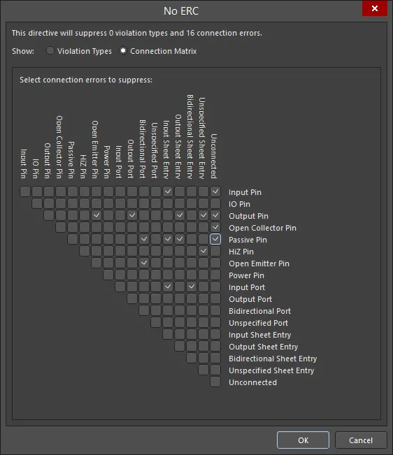
The No ERC dialog showing Violation Types mode (the first image) and Connection Matrix mode (the second image)
К диалогу можно получить доступ, щёлкнув Specific Violations в области Suppressed Violations region панели Properties panel в режиме No ERC mode (упомянутом выше).

Options and Controls of the No ERC Dialog
-
Top statement - Это сообщение позволяет быстро увидеть, сколько типов нарушений и ошибок соединений сейчас подавлено. Сообщение обновляется по мере внесения изменений в диалоге.
-
Show - выберите Violation Types или Connection Matrix, чтобы просмотреть и настроить соответствующую директиву No ERC.
Типы нарушений
Этот режим позволяет подавлять или отменять подавление типов нарушений.
-
Violation Type To Suppress - отображает список типов нарушений, доступных для настройки.
-
Report Mode - отображает текущий режим отчёта для указанного типа нарушения.
-
Suppress - установите флажок, чтобы подавить соответствующий тип нарушения; снимите флажок, чтобы отменить подавление.
Меню правой кнопки мыши
Значение [xxx] в следующих командах контекстного меню будет меняться в зависимости от типа нарушения, который был выбран (или над которым находился курсор) в момент щелчка правой кнопкой.
Также можно щёлкнуть правой кнопкой по записи Violations Associated with, чтобы получить доступ к командам контекстного меню для всего объекта.
-
Suppress only "[xxx]" - используйте, чтобы подавить только те типы нарушений, которые перечислены в кавычках.
-
Unsuppress only "[xxx]" - используйте, чтобы отменить подавление только тех типов нарушений, которые перечислены в кавычках.
-
Suppress All "[xxx]" - используйте, чтобы подавить все типы нарушений объекта, указанного в кавычках.
-
Unsuppress All "[xxx]" - используйте, чтобы отменить подавление всех типов нарушений объекта, указанного в кавычках.
-
Suppress All - используйте, чтобы подавить все перечисленные типы нарушений независимо от объекта или положения курсора.
-
Unsuppress All - используйте, чтобы отменить подавление всех перечисленных типов нарушений независимо от объекта или положения курсора.
-
Toggle All - используйте, чтобы переключить флажок Suppress checkbox у всех типов нарушений.
Матрица соединений
Этот режим позволяет подавлять или отменять подавление ошибок соединений.
-
Grid - используйте флажки в таблице, чтобы подавить (флажок установлен) или отменить подавление (флажок снят) нужных ошибок соединений.
При наведении на флажок он и соответствующие соединения выделяются жирным, что упрощает обновление нужных ошибок соединений.
Меню правой кнопки мыши
Значение [xxx] в следующих командах контекстного меню будет меняться в зависимости от ошибки соединения, которая была выбрана (или над которой находился курсор) в момент щелчка правой кнопкой.
-
Suppress only "[xxx]" - используйте, чтобы подавить только те ошибки соединений, которые перечислены в кавычках.
-
Unsuppress only "[xxx]" - используйте, чтобы отменить подавление только тех ошибок соединений, которые перечислены в кавычках.
-
Suppress All "[xxx]" - используйте, чтобы подавить все ошибки соединений, указанные в кавычках. Таких команд две — по одной для каждой части соединения.
-
Unsuppress All "[xxx]" - используйте, чтобы отменить подавление всех ошибок соединений, указанных в кавычках. Таких команд две — по одной для каждой части соединения.
-
Suppress All - используйте, чтобы подавить все ошибки соединений в таблице.
-
Unsuppress All - используйте, чтобы отменить подавление всех ошибок соединений в таблице.
-
Toggle All - используйте, чтобы переключить флажок у всех ошибок соединений. Установленные флажки будут сняты; снятые — установлены.
Конкретную (Specific) директиву No ERC можно настроить на несколько нарушений, чтобы поддерживать схемы, которые будут генерировать несколько ошибок/предупреждений.
-
Через панели SCH List и SCH Filter panels. Панель List panel позволяет отображать объекты проекта из одного или нескольких документов в табличном виде, обеспечивая быструю проверку и изменение атрибутов объектов. При использовании совместно с соответствующей фильтрацией — через панель Filter panel или диалог Find Similar Objects dialog — это позволяет отображать только те объекты, которые попадают в область действия активного фильтра, давая возможность более точно и эффективно выбирать и редактировать сразу несколько объектов проекта.

Общую (Generic) директиву No ERC можно быстро переключить в конкретную (Specific) директиву No ERC и наоборот — либо через панель Properties panel (в разделе Suppressed Violations section), либо переключив свойство Suppress Specific Violations property на панели SCH List panel.
Деактивация директивы No ERC
Вместо удаления директивы No ERC ее можно сделать неактивной (то есть отключенной с точки зрения проверки). Это состояние изменяется переключением свойства директивы Active — доступного через любой из способов редактирования. Неактивная директива No ERC будет отображаться серым цветом в рабочей области проекта.

Если нужно временно прекратить использование директивы No ERC, сделайте ее неактивной, а не удаляйте.
Управление печатью директив No ERC
По умолчанию маркеры No ERC включаются при печати. Чтобы управлять этим — либо полностью отключив их вывод, либо исключив только определенные символы, используйте диалог печати как показано ниже.

Управляйте печатью маркеров No ERC в Print диалоге.
No ERC
 Используйте маркеры No ERC, чтобы подавлять сообщения об ошибках/предупреждениях для конкретного узла в схеме.
Сводка
Объект No ERC — это директива проектирования. Он размещается на узле схемы, чтобы подавить все предупреждения и/или ошибки Electrical Rule Check, которые обнаруживаются при компиляции проекта схемы. Используйте No ERC, чтобы намеренно ограничить проверку ошибок в определенной точке схемы, о которой вы знаете, что она будет генерировать предупреждение (например, неподключенный вывод), при этом сохраняя комплексную проверку остальной части схемы.
Директива No ERC поддерживает несколько различных стилей и может отображаться любым цветом. Используйте это, чтобы отражать замысел проектирования для данной точки схемы.
Выберите стиль No ERC, который лучше всего отражает его назначение в этой точке схемы.
Директива No ERC имеет два типа:
-
All Violations – подавляются все возможные предупреждения и/или ошибки.
-
Specific Violations – подавляются только выбранные предупреждения или ошибки; любые другие предупреждения или ошибки будут обнаружены и выведены.
Доступность
Директивы No ERC доступны для размещения только в редакторе схем. Чтобы разместить директиву No ERC:
-
Нажмите Place » Directives » Generic No ERC в главном меню, чтобы разместить маркер No ERC, предварительно настроенный на подавление всех нарушений. Иногда это называют универсальной (Generic) директивой No ERC.
-
Щелкните правой кнопкой мыши в редакторе схем, затем выберите Place » Directives » Generic No ERC.
Размещение — универсальная директива No ERC
После запуска команды курсор изменится на перекрестие, и вы перейдете в режим размещения. Выполните следующее, чтобы разместить директиву No ERC:
-
Наведите курсор на провод или другой объект цепи (net), затем щелкните Enter , чтобы разместить директиву в этой точке схемы.
-
Продолжайте размещать дополнительные директивы No ERC либо щелкните правой кнопкой мыши или нажмите Esc , чтобы выйти из режима размещения.
Дополнительные действия, которые можно выполнять во время размещения:
-
Нажмите клавишу Tab, чтобы приостановить размещение и открыть режим No ERC панели Properties, где можно изменять свойства «на лету». Нажмите кнопку паузы-оверлея в рабочей области, чтобы продолжить размещение.
Хотя атрибуты можно изменять во время размещения (
Tab для доступа к
Properties панели), имейте в виду, что они станут настройками по умолчанию для последующего размещения, если только не включена опция
Permanent на странице
Schematic – Defaults диалога
Preferences . Когда эта опция включена, внесенные изменения будут влиять только на размещаемый объект и последующие объекты, размещенные в рамках той же сессии размещения.
Графическое редактирование
Маркёр No ERC нельзя изменять графически, кроме изменения его положения. Чтобы переместить маркер No ERC, щелкните и удерживайте, перетаскивая его в новое место.
Если попытаться графически изменить объект, у которого включено свойство Locked, появится диалог с запросом подтверждения продолжения редактирования. Если опция Protect Locked Objects включена на странице Schematic – Graphical Editing диалога Preferences , и при этом также включена опция Locked для данного объекта проектирования, то этот объект нельзя выбрать или графически редактировать. Щелкните по заблокированному объекту, чтобы выбрать его, затем отключите свойство Locked в List панели или отключите опцию Protect Locked Objects , чтобы получить возможность графически редактировать объект.
Неграфическое редактирование
Доступны следующие способы неграфического редактирования.
Редактирование через диалог No ERC или панель Properties
Panel page: Свойства No ERCЭтот способ редактирования использует связанный диалог No ERC и режим Properties панели для изменения свойств объекта.

 No ERC Диалог (первое изображение) и режим No ERC панели Properties (второе изображение)
После размещения доступ к No ERC диалогу можно получить:
-
Дважды щелкнув по размещенному объекту No ERC.
-
Наведя курсор на объект No ERC, щелкнув правой кнопкой мыши и выбрав Properties в контекстном меню.
Во время размещения режим No ERC Propertiesпанели можно открыть, нажав клавишу Tab. После размещения No ERC отображаются все параметры.
После размещения режим No ERC Propertiesпанели можно открыть одним из следующих способов:
-
Если Propertiesпанель уже активна — выбрав объект No ERC.
-
После выбора объекта No ERC выберите Properties панель с помощью Panels кнопки в правом нижнем углу рабочей области или выберите View » Panels » Properties в главном меню.
Если опция
Double Click Runs Interactive Properties отключена (по умолчанию) на странице
Schematic - Graphical Editing диалога
Preferences , то при двойном щелчке по примитиву или при щелчке правой кнопкой мыши по выбранному примитиву с последующим выбором
Properties откроется диалог. Когда опция
Double Click Runs Interactive Properties включена, откроется
Properties панель.
Хотя параметры в диалоге и панели одинаковы, их порядок и расположение могут немного отличаться.
К свойствам можно получить доступ до входа в режим размещения на странице
Schematic – Defaults page диалога
Preferences . Это позволяет изменить свойства объекта по умолчанию, которые будут применяться при размещении последующих объектов.
Редактирование через связанный диалог свойств
Этот способ редактирования использует диалог No ERC для изменения типов нарушений и ошибок соединения для конкретного (Specific) объекта No ERC.
 и режим Connection Matrix (второе изображение)")
 No ErcДиалог, показывающий режим Violation Types (первое изображение) и режим Connection Matrix (второе изображение)
Доступ к диалогу можно получить, нажав Specific Violations в области Suppressed Violations диалога No ERC и в Properties панели в режиме No ERC .
Конкретную (Specific) директиву No ERC можно настроить на несколько нарушений, чтобы поддерживать схемы, которые будут генерировать несколько ошибок/предупреждений.
Редактирование нескольких объектов
PropertiesПанель поддерживает редактирование нескольких объектов, при котором можно изменять настройки свойств, одинаковые для всех выбранных объектов. Когда несколько объектов одного типа выбраны вручную, через диалог Find Similar Objects или через панель SCH Filter или панель SCH List, поле Properties панели, значение которого не отображается как звездочка (*), можно редактировать для всех выбранных объектов.

Редактирование через панель списка
Panel pages: SCH List, SCH Filter
Панель List позволяет отображать объекты проектирования из одного или нескольких документов в табличном виде, обеспечивая быстрый просмотр и изменение атрибутов объектов. При использовании совместно с соответствующей фильтрацией — через нужную Filter панель или диалог Find Similar Objects — она позволяет отображать только те объекты, которые попадают в область действия активного фильтра, что дает возможность более точно и эффективно выбирать и редактировать несколько объектов проектирования.
No ERC Properties
Свойства объектов редактора схем — это настраиваемые параметры, определяющие визуальный стиль, содержимое и поведение размещенного объекта. Настройки свойств для каждого типа объектов задаются двумя разными способами:
-
Pre-placement settings – большинство свойств объекта No ERC, или тех, которые логично предопределить, доступны как редактируемые значения по умолчанию на странице Schematic - Defaults диалога Preferences (доступ через кнопку
 в правом верхнем углу рабочей области). Выберите объект в Primitive List , чтобы справа отобразились его параметры.

-
Post-placement settings – все свойства объекта No ERC доступны для редактирования в No ERC диалоге и Propertiesпанели, когда размещенный No ERC выбран в рабочей области.

Если параметр
Double Click Runs Interactive Properties отключен (по умолчанию) на странице
Schematic - Graphical Editing page в
Preferences dialog, то при двойном щелчке по примитиву или при щелчке правой кнопкой мыши по выбранному примитиву с последующим выбором
Properties откроется диалоговое окно. Если параметр
Double Click Runs Interactive Properties включен, откроется
Properties p
anel.
Хотя параметры в диалоге и в панели одинаковые, порядок и расположение параметров могут немного отличаться.
В приведенном ниже списке свойств параметры, которые недоступны в качестве настроек по умолчанию в Preferences dialog, помечены как "Properties panel only".
Расположение (Properties panel only)
-
(X/Y)
-
X (первое поле) — текущая координата X (горизонтальная) опорной точки объекта относительно текущего начала координат рабочего пространства проекта. Измените, чтобы поменять положение объекта по X. Значение можно вводить как в метрических, так и в дюймовых единицах; указывайте единицы измерения при вводе значения, если они отличаются от текущих единиц по умолчанию.
-
Y (второе поле) — текущая координата Y (вертикальная) опорной точки объекта относительно текущего начала координат. Измените, чтобы поменять положение объекта по Y. Значение можно вводить как в метрических, так и в дюймовых единицах; указывайте единицы измерения при вводе значения, если они отличаются от текущих единиц по умолчанию.
-
Rotation - используйте раскрывающийся список, чтобы выбрать поворот.
Свойства
-
Color — щелкните по цветному полю, чтобы открыть раскрывающийся список, в котором можно выбрать цвет по умолчанию.
-
Symbol - используйте раскрывающийся список, чтобы выбрать значение по умолчанию из доступных вариантов.
-
Active - включите, чтобы сделать примитив активным.
Подавленные нарушения (Properties panel only)
-
All Violations — выберите, чтобы отображать все нарушения для этого объекта. Violation Type и Report Mode для нарушений отображаются в таблице.
-
Specific Violations - выберите, чтобы отображать конкретные нарушения для этого объекта. Violation Type и Report Mode для нарушений отображаются в таблице.
-
Add - нажмите, чтобы открыть диалог No ERC и добавить новое нарушение. После нажатия OK новое нарушение будет добавлено в таблицу. Нажмите
 чтобы удалить текущее выбранное нарушение.
Типы нарушений правил проектирования PCB
Нарушения, связанные с шинами
Bus indices out of range
Это нарушение возникает, когда индекс входящей в состав сети, подключенной к шине, выходит за пределы диапазона, заданного сетью, с которой связана шина.
Уведомление в панели Messages
Уведомление отображается в панели Messages в следующем формате:
Bus index out of range on <NetPrefix> Index = <NetIndex>
где:
-
NetPrefix — префикс входящей в состав сети, подключенной к шине (например, A для сети A8, подключенной к шине, связанной с сетью A[0..7]).
-
NetIndex — ошибочный индекс входящей в состав сети (например, сеть A8 имеет индекс 8).
Рекомендации по устранению
Либо исправьте индекс проблемной сети так, чтобы он находился в правильном диапазоне, либо переименуйте сеть полностью. Второй вариант типичен, если вы назвали сеть по ошибке и она не является составляющей сети, передаваемой объектом шины.
Bus range syntax errors
Это нарушение возникает, когда синтаксис сети, с которой связана шина, задан неверно.
Уведомление в панели Messages
Уведомление отображается в панели Messages в следующем формате:
Bus range syntax error <NetName> at <Location>
где:
-
NetName — имя родительской сети, с которой связан проблемный объект шины.
-
Location — координаты X, Y электрической «горячей точки» проблемного объекта шины.
Рекомендации по устранению
Корректно задайте синтаксис шины для проблемного идентификатора сети (например, метка сети, порт, вход листа и т. п.). Правильный синтаксис должен соответствовать одному из следующих форматов:
-
NetName[LowerIndex..UpperIndex]
-
NetName[UpperIndex..LowerIndex]
Например, рассмотрим шину, которая переносит две входящие в состав сети: A0 и A1. В этом случае синтаксис шины должен быть A[0..1] или A[1..0]. Примеры неверного синтаксиса: A[0.1], A[1-0], A[0,1], A[..1] и A[0..].
Illegal bus range values
Это нарушение возникает, когда по крайней мере один индекс в синтаксисе сети, связанной с шиной, имеет отрицательное значение.
Уведомление в панели Messages
Уведомление отображается в панели Messages в следующем формате:
Illegal bus range value <BusLabel> at <Location>
где:
-
BusLabel — заданная маркировка шины, в которой обнаружено недопустимое значение.
-
Location — координаты X, Y электрической «горячей точки» проблемного объекта шины.
Рекомендации по устранению
Корректно задайте синтаксис шины для проблемного идентификатора сети (например, метка сети, порт, вход листа и т. п.). Правильный синтаксис должен соответствовать одному из следующих форматов:
-
<NetName>[<LowerIndex>..<UpperIndex>]
-
<NetName>[<UpperIndex>..<LowerIndex>]
LowerIndex и UpperIndex могут быть равны нулю или быть положительным целым числом, но не могут быть отрицательными.
Mismatched bus label ordering
Это нарушение возникает, когда два идентификатора сети, связанные с одним и тем же срезом шины, задают метки шины с порядком, направленным не в одну и ту же сторону (по возрастанию или по убыванию).
Уведомление в панели Messages
Уведомление отображается в панели Messages в следующем формате:
Mismatched bus ordering on <NetName> Low value first and High value first
где:
-
NetName — имя родительской сети, с которой связано несоответствие порядка шины.
Рекомендации по устранению
Определите идентификаторы сети (порт, метка сети, вход листа и т. п.), у которых порядок шины не согласован. Определите правильный порядок и исправьте именование ошибочного объекта.
Mismatched bus widths
Это нарушение возникает, когда два идентификатора сети, связанные с одним и тем же срезом шины, задают метки шины разной ширины. Например, порт с именем A[0..7] может быть подключен к шине, у которой присоединенная метка сети определена как A[0..15].
Уведомление в панели Messages
Уведомление отображается в панели Messages в следующем формате:
Mismatched bus widths on bus section <NetName> (<BusSize1> and <BusSize2>)
где:
-
NetName — имя родительской сети, с которой связаны несоответствующие объекты шины.
-
BusSize1 — ширина первого из проблемных объектов шины.
-
BusSize2 — ширина второго из проблемных объектов шины.
Рекомендации по устранению
Определите идентификаторы сети (порт, метка сети, вход листа и т. п.), ширина меток шины у которых не согласована. Определите правильную ширину и исправьте именование ошибочного объекта.
Mismatched Bus/Wire object on Wire/Bus
Это нарушение возникает, когда объект «провод» неправильно подключен к шине или объект «шина» неправильно подключен к проводу. Например, порт A может быть подключен к шине, но для имени порта не задан правильный синтаксис метки шины (например, A[0..1]). По сути, порт является объектом одиночного сигнала (или провода), который теперь ошибочно подключен к шине.
Уведомление в панели Messages
Уведомление отображается в панели Messages в следующем формате:
<ObjectIdentifier> at <Location> placed on a <ObjectType>
где:
-
ObjectIdentifier представляет несоответствующий объект, который может быть либо шиной, либо проводом (например, вывод, порт, порт питания, метка сети, межлистовой соединитель, вход листа). Идентификатор будет отображаться в одном из следующих двух форматов:
-
Для шины —
Bus <Object> <Name> (например, Bus Net Label GND_BUS[..]).
-
Для провода —
Wire <Object> <Name> (например, Wire Port TXD).
-
Location — координаты X,Y электрической «горячей точки» объекта.
-
ObjectType — объект, на котором размещен проблемный объект — либо провод, либо шина.
Рекомендации по устранению
Чтобы устранить проблему, рассмотрите следующее:
-
Is the connection correct? – действительно ли шина, подключаемая к объекту, должна быть проводом, и наоборот?
-
Is the object defined correctly? – для объекта шины убедитесь, что имя объекта задано с использованием правильного синтаксиса шины в виде
<Name>[<LowIndex>..<HighIndex>] или <Name>[<HighIndex>..<LowIndex>]. Например, выходной порт данных шириной в байт может быть задан как DAT_OUT[7..0]. Для объекта провода убедитесь, что имя объекта определяет одиночный сигнал и не задано с использованием синтаксиса шины.
Mixed generic and numeric bus labeling
Это нарушение возникает, когда два идентификатора сети (порт, метка сети, вход листа и т. п.), подключенные к одному и тому же срезу шины, различаются по синтаксису шины — один задает диапазон шины в числовом формате (например, A[0..2]), а другой задает диапазон в обобщенном формате (например, A[0..b]).
Уведомление в панели Messages
Уведомление отображается в панели Messages в следующем формате:
Mismatched generic and numeric bus labeling on <NetName> <Level> value first and Generic
где:
-
NetName— это имя родительской цепи (parent net), с которой связано несоответствие в маркировке шины.
-
Level зависит от числового порядка для цепи. Если по возрастанию (например, [0..2]), то Level будет отображаться как Low. Если по убыванию (например, [2..0]), то Level будет отображаться как High.
Рекомендация по устранению
Определите, какой из проблемных объектов содержит ошибку в задании метки шины, и исправьте её соответствующим образом.
Использование обобщений (Generics) в именах шин не поддерживается. Убедитесь, что вместо них используются числовые значения.
Нарушения, связанные с компонентами
Component has been deleted
Это нарушение возникает, когда из проектной разработки был удалён как минимум один компонент. Удаление выполняется в режиме «мягкого удаления» (soft delete): удалённые компоненты перемещаются в специальное Trash место, откуда их можно восстановить (Restore) или полностью удалить (Permanently Delete) через пункты меню удалённой записи (⋯) в браузерном интерфейсе подключённого Workspace.
Уведомление в панели Messages
Уведомление отображается в панели Messages в следующем формате:
ComponentName: Component has been deleted
где:
-
ComponentName — имя компонента Workspace.
Рекомендация по устранению
Если компонент был удалён по ошибке, его может восстановить пользователь с соответствующими правами доступа на странице Trash в браузерном интерфейсе Workspace. В противном случае замените компонент, используемый в проекте, на другой эквивалентный компонент, который is доступен в подключённом Workspace.
Component Implementations with invalid pin mappings
Это нарушение возникает при компиляции Integrated Library Package (*.LibPkg), когда обнаруживается некорректное сопоставление выводов (pin mapping) между компонентом схемы и связанным с ним моделем.
Уведомление в панели Messages
Уведомление отображается в панели Messages в следующем формате:
ComponentName: Could not find port <ModelPinNumber> on model <ModelName> for pin <ComponentPinNumber> – относится к PCB-модели
ComponentName: Could not map port <ModelPinNumber> on model <ModelName> to a pin – относится к модели симуляции
где:
-
ComponentName — имя компонента в исходной библиотеке схем.
-
ModelPinNumber — ожидаемое обозначение вывода/площадки (pin/pad), которое не удалось найти в связанном моделе.
-
ModelName — имя модели, связанной с компонентом.
-
ComponentPinNumber — обозначение вывода на исходном компоненте схемы, к которому привязан ошибочный вывод модели.
Рекомендация по устранению
Устранение заключается в проверке сопоставления между условным графическим обозначением (schematic symbol) и моделью целевого домена. Для этого сначала нужно открыть свойства соответствующего компонента библиотеки схем. Дважды щёлкните по записи компонента в списке Components панели SCH Library panel, чтобы открыть панель Properties panel с загруженными свойствами этого компонента.
Если отображается сообщение о нарушении, связанном с PCB-моделью, выберите модель в разделе Footprint панели и нажмите кнопку  под списком, чтобы открыть диалог PCB Model dialog. Затем нажмите кнопку Pin Map, чтобы открыть диалог Model Map dialog. В столбце Component Pin Designator найдите номер вывода, отмеченный в сообщении (
ComponentPinNumber). Нарушение возникает потому, что соответствующая запись в столбце Model Pin Designator указывает на обозначение площадки, которого нет в PCB-модели. Исправьте запись соответствующим образом. Обычно сопоставление «один к одному», и обозначения с обеих сторон совпадают.
Если отображается сообщение, связанное с моделью симуляции, выберите модель в разделе Models панели и нажмите кнопку под списком, чтобы открыть диалог Sim Model. Затем перейдите на вкладку Port Map. Это нарушение возникает, когда вывод модели некорректно сопоставлен выводу компонента схемы. Такое может произойти, если для вывода модели задан вывод, который уже сопоставлен, либо задано значение Not Connected. Исправьте запись соответствующим образом.
Component revision has inapplicable state
Это нарушение возникает, когда обнаруживается, что как минимум один размещённый экземпляр ревизии Component Item Revision — размещённый из подключённого Workspace — находится в неприменимом состоянии. Например, компонент сейчас имеет состояние Depracated или Obsolete и поэтому не должен присутствовать в последней итерации проекта. Применимость определяется через опцию Allowed to be used in designs в диалоге State Properties dialog. Из диалога Edit Lifecycle Definitions dialog откройте этот диалог для нужного состояния — либо двойным щелчком по записи состояния в родительском определении жизненного цикла, либо выбрав запись и нажав появляющийся значок редактирования ( ). Когда эта опция включена, Item Revision в данном состоянии разрешено использовать в проекте. Он считается Applicable. Если опция отключена, Item Revision в данном состоянии нельзя корректно использовать, и он считается Inapplicable (или неприменимым).
Диалог
Edit Lifecycle Definitions открывается со страницы
Data Management – Servers page диалога
Preferences, нажатием кнопки
Properties для Workspace, в который выполнен активный вход, затем выбором
Lifecycles в выпадающем меню.
Уведомление в панели Messages
Уведомление отображается в панели Messages в следующем формате:
Component <Designator> <Comment>: Component revision has inapplicable state
где:
-
Designator — Designator экземпляра компонента.
-
Comment — Comment экземпляра компонента.
Рекомендация по устранению
Используйте диалог Item Manager dialog, чтобы выбрать замену — ревизию Component Item Revision, допустимую для использования в проекте. Сделайте это для каждого компонента, находящегося в неприменимом состоянии. Либо можно заменить текущую ревизию Component Item Revision на другую ревизию или на ревизию другого Component Item на уровне отдельного компонента. Выберите компонент на схеме, чтобы открыть его свойства в панели Properties panel. В разделе Properties панели либо нажмите кнопку Update, чтобы использовать последнюю ревизию текущего Component Item, либо нажмите кнопку  справа от поля Design Item ID, чтобы открыть ваш Workspace и выбрать другую ревизию Component Item Revision.
Используйте элементы управления, доступные через панель Properties или диалог Item Manager, чтобы выбрать более позднюю ревизию элемента, которая is находится в применимом состоянии, или, если это невозможно (элемент в целом не предназначен для использования в проектировании), выберите применимую ревизию другого элемента.
Примечания
-
Если размещённый компонент теряет связь со своим исходным Workspace — например, Workspace, из которого он был размещён, отключён или вы вышли из Workspace — он будет нарушать проверку Component revision has inapplicable state. Это будет отражено в панели Messages записью вида: Component <Designator> <Comment>: Can't perform revision status validation: Failed to get session: Access denied! User login required for this service.
-
Также можно выявлять компоненты, которые используются в проекте некорректно, в процессе выпуска (release) проекта. Добавьте и настройте Component State Checking в общий регламент проверок (validation) выпуска.
Component revision is Out of Date
Это нарушение возникает, когда обнаруживается, что компонент — размещённый из подключённого Workspace — устарел (не является актуальной ревизией).
Уведомление в панели Messages
Уведомление отображается в панели Messages в следующем формате:
Component <Designator> at <Location>: Component revision is Out of Date
где:
-
Designator — Designator экземпляра компонента.
-
Location — координаты X, Y, отмечающие начало координат (origin) проблемного экземпляра компонента.
Рекомендация по устранению
Используйте диалог Item Manager dialog, чтобы определить и обновить компоненты, которые не являются последней ревизией. В Item Manager есть столбец Revision Status; для компонентов, которые не на последней ревизии, статус компонента будет Out of Date. Выберите устаревший(е) компонент(ы), щёлкните правой кнопкой мыши и выберите Update to latest revision в меню. После этого Generate выполните ECO, чтобы применить изменения к затронутым схемам.
В качестве альтернативы можно заменить текущую ревизию Component Item Revision на последнюю ревизию на уровне отдельного компонента. Просто выберите компонент на схеме, чтобы открыть его свойства в панели Properties panel. В разделе Properties панели нажмите кнопку Update, чтобы использовать последнюю ревизию текущего Component Item.
Примечание
Если размещённый компонент теряет связь со своим исходным Workspace — например, Workspace, из которого он был размещён, отключён или вы вышли из Workspace — он будет нарушать проверку Component revision is Out of Date. Это будет отражено в панели Messages записью вида: Component <Designator> <Comment>: Can't perform revision status validation: Failed to get session: Access denied! User login required for this service.
Компоненты, содержащие дублирующиеся подчасти
Это нарушение возникает, когда одна и та же часть (секция) многосекционного компонента была размещена в схеме более одного раза. Например, вы разместили компонент 74HC32 с обозначением U9, но по ошибке разместили два экземпляра первой части этого компонента, в результате чего в проекте оказалось два экземпляра U9A.
Уведомление в панели Messages
Уведомление отображается в панели Messages в следующем формате:
Component <ComponentName> has duplicate sub-parts at <Location1> and <Location2>
где:
-
ComponentName — имя проблемного компонента в терминах его позиционного обозначения и ссылки на библиотеку.
-
Location1 — координаты X, Y для первого экземпляра соответствующей подчасти.
-
Location2 — координаты X, Y для дублирующего экземпляра соответствующей подчасти.
Рекомендации по устранению
Измените номер части (part number) для проблемных частей по необходимости, используя команду Increment Part Number — доступную из главного меню Edit или из подменю Part Actions (при щелчке правой кнопкой по части). Преимущество запуска команды из меню Edit в том, что вы остаётесь в режиме инкремента, что позволяет циклически переключать номера частей, пока не будет выбран нужный.
Компоненты с дублирующимися выводами
Это нарушение возникает, когда два или более выводов компонента имеют одинаковое обозначение.
Уведомление в панели Messages
Уведомление отображается в панели Messages в следующем формате:
Duplicate pins in component Pin <Identifier1> and Pin <Identifier2>
где:
-
Identifier1 — идентификатор первого экземпляра дублирующегося вывода, представленный парой «обозначение части — обозначение вывода»
-
Identifier2 — идентификатор второго экземпляра дублирующегося вывода, представленный парой «обозначение части — обозначение вывода».
Рекомендации по устранению
Соответствующим образом измените обозначение проблемного(ых) вывода(ов), чтобы у каждого было уникальное назначение. Обозначения выводов можно редактировать в редакторе схемы для уже размещённого компонента:
-
Если выводы компонента не заблокированы, можно просто выбрать вывод и отредактировать его обозначение через панель Properties.
-
В противном случае отредактируйте вывод(ы) с помощью диалога Component Pin Editor. При выбранном компоненте в рабочей области доступ к этому диалогу осуществляется из панели Properties нажатием кнопки ниже раздела Pins на вкладке Pins панели.
Обычно дублирование находится в библиотечном компоненте; в этом случае следует отредактировать обозначение вывода для этого компонента в исходной библиотеке схем, а затем передать изменение в размещённые экземпляры компонента, используя команды Update From Libraries (Schematic Editor) или Update Schematics (Schematic Library Editor). Обе команды доступны из главных меню Tools соответствующих редакторов.
Примечание
Для каждого отдельного компонента в панели Messages будет перечислен только один экземпляр нарушения. У компонента может быть более двух выводов с одинаковым обозначением, но при исследовании нарушения с помощью области Details панели будут перечислены только первые два дублирующихся вывода (в алфавитном порядке имён выводов).
Дублирующиеся позиционные обозначения частей
Это нарушение возникает, когда как минимум две части на исходных листах схем проекта имеют одинаковое позиционное обозначение.
Уведомление в панели Messages
Уведомление отображается в панели Messages в следующем формате:
Duplicate Component Designators <PartDesignator>
где:
-
PartDesignator — проблемное позиционное обозначение.
Рекомендации по устранению
Назначьте дубликатам разные и уникальные позиционные обозначения. Это можно сделать вручную, отредактировав каждое проблемное обозначение, либо с помощью диалога Annotate (Tools » Annotation » Annotate Schematics).
Либо сначала сбросьте дублирующиеся позиционные обозначения компонентов с помощью команды Tools » Annotation » Reset Duplicate Schematic Designators, затем используйте команду Tools » Annotation » Annotate Schematics Quietly для аннотирования без запуска диалога Annotate .
Обобщённый компонент
Это нарушение возникает, когда в финальный проект включён Generic Component. Generic Components можно быстро размещать в проекте без необходимости искать и выбирать конкретную деталь производителя из доступных источников компонентов; они предназначены как заполнители, которые легко заменить подходящим компонентом.
Уведомление в панели Messages
Уведомление отображается в панели Messages в следующем формате:
Generic Component <PartDesignator> is placed at <Location>
где:
-
Designator — Designator размещённого экземпляра обобщённого компонента.
-
Location — координаты X, Y, отмечающие начало координат проблемного экземпляра обобщённого компонента.
Рекомендации по устранению
Когда проект продвинулся до стадии, на которой Generic Component можно заменить конкретным физическим компонентом, можно использовать диалог Replace Component, выбрав меню с многоточием в Design Item ID field панели Properties. Обратите внимание: это также можно сделать из Item Manager или через документ проекта ActiveBOM.
Несоответствие соединений скрытых выводов
Это нарушение возникает в многосекционных компонентах, когда скрытый вывод, общий для более чем одной подчасти, подключён к разным цепям (net).
Уведомление в панели Messages
Уведомление отображается в панели Messages в следующем формате:
Mismatched hidden pin connections in Pin <Identifier> and Pin <Identifier>
где:
-
Identifier — используется для идентификации рассматриваемого вывода. Идентификатор отображается в формате PhysicalComponentName-PinDesignator (например, U2-7).
Рекомендации по устранению
Переназначьте проблемный(е) вывод(ы) на правильные цепи. Скрытый вывод назначается цепи путём ввода имени цепи в поле Hidden Net Name в соответствующей панели List (SCHLIB List panel или SCH List panel), когда панель отображает свойства вывода. Если это выполняется в панели SCH List, щёлкните правой кнопкой в панели и включите опцию Show Children, чтобы выводы отображались списком в панели.
Несоответствие видимости выводов
Это нарушение связано с выводами питания (VCC и GND) многосекционного компонента. Обычно эти выводы относятся к части 0, автоматически подключаются к цепям VCC и GND проекта и скрыты. Если для одной из частей компонента включить видимость такого вывода, он перестаёт быть подключённым к целевой цепи питания, и будет отмечена ошибка.
Уведомление в панели Messages
Уведомление отображается в панели Messages в следующем формате:
Pin is visible in one sub-part and hidden in another sub-part
Рекомендации по устранению
Либо отключите отображение проблемного(ых) вывода(ов) питания в рабочей области, либо, если оставляете выводы видимыми, убедитесь, что к выводу(ам) соответствующим образом подключён объект порта питания VCC и/или GND.
Отсутствующие модели компонентов
Это нарушение возникает при компиляции пакета Integrated Library Package (*.LibPkg), когда не удаётся найти связанную модель для компонента в исходной библиотеке схем.
Уведомление в панели Messages
Когда связанная модель является моделью посадочного места (footprint) или моделью симуляции, уведомление отображается в панели Messages в одном из следующих форматов:
<ComponentName>: Could not find <ModelName> — когда область поиска модели: Any.
<ComponentName>: Could not find <ModelName> in <LibraryName> — когда область поиска модели: Library Name.
<ComponentName>: Could not find <ModelName> in <Path> — когда область поиска модели: Library Path.
где:
-
ComponentName — имя компонента в исходной библиотеке схем.
-
ModelName — имя посадочного места или модели симуляции, связанной с исходным компонентом, которую не удалось найти.
-
LibraryName — имя файла библиотеки, в котором указано, что должна находиться связанная модель.
-
Path — абсолютный путь к файлу библиотеки, в котором указано, что должна находиться связанная модель.
Когда связанная модель является моделью целостности сигнала, сообщение отображается на панели Messages в следующем формате:
<ComponentName>: Could not find 'GenericEntity' in <Path>
где:
-
ComponentName — имя компонента в исходной библиотеке схем.
-
Path — абсолютный путь к библиотеке/модели.
Рекомендации по устранению
Когда проблема связана с привязанным посадочным местом или моделью симуляции
Эта проблема обычно вызвана одним из следующих сценариев:
-
Имя модели указано неверно при определении ссылки на модель.
-
Связанная модель не находится в указанном файле библиотеки.
-
Файл библиотеки, содержащий связанную модель, был перемещён или удалён.
Первый шаг при устранении этого нарушения — соответствующее диалоговое окно настройки для типа модели, на которую вы ссылаетесь: диалог PCB Model dialog или диалог Sim Model. В каждом случае проверьте и убедитесь, что:
-
Имя модели, на которую вы ссылаетесь, указано правильно, и
-
Для поиска файла библиотеки/модели, в котором находится эта модель, используется правильный вариант.
Формат отображаемого сообщения об ошибке зависит от включённой области поиска при обнаружении модели и может существенно помочь при поиске проблемы со ссылкой на модель:
-
Если модель не удалось найти по указанному пути (область поиска:
Library path), убедитесь, что указанный файл библиотеки/модели действительно существует в этом месте, а также проверьте файл библиотеки/модели на наличие модели с указанным именем.
-
Если модель не удалось найти в указанном файле библиотеки/модели (область поиска:
Library name), убедитесь, что файл библиотеки/модели добавлен в список Available Libraries (Project Libraries, Installed Libraries, Project Search Paths). Также проверьте, что файл библиотеки/модели содержит модель с тем же именем, которое указано в ссылке.
-
Если модель просто не удалось найти (область поиска:
Any), убедитесь, что в список Available Libraries добавлен файл библиотеки/модели, содержащий модель с тем же именем, что указано в ссылке.
Когда проблема связана с привязанной моделью целостности сигнала
Обычно это вызвано тем, что не указан тип модели целостности сигнала (например, диод, ИС). Это устраняется в соответствующем диалоговом окне настройки моделей целостности сигнала. Проще всего открыть его через панель Properties panel при просмотре свойств выбранного компонента. Проверьте, что в разделе Models на вкладке General панели используется правильная модель, и при необходимости исправьте. Кнопки Add and можно использовать для создания новой модели (выберите Signal Integrity из списка) или изменения существующей модели целостности сигнала. Это откроет диалог Signal Integrity Model, где кнопка Import Ibis позволяет импортировать модели выводов из файла модели Ibis.
Вы можете добавить модель Ibis напрямую, нажав Add » Ibis model и используя последующее диалоговое окно Ibis Model для задания ссылки на модель и файл.
Missing pin found in component display mode
Это нарушение возникает, если в одном из режимов отображения компонента обнаружен отсутствующий вывод.
Уведомление на панели Messages
Уведомление отображается на панели Messages в следующем формате:
<NumberOfMissingPins> missing pins in <DisplayMode> of design item <DesignItemID>
где:
-
NumberOfMissingPins — количество отсутствующих выводов, найденных в компоненте.
-
DisplayMode — конкретный режим графического представления компонента, в котором обнаружен(ы) отсутствующий(ие) вывод(ы). Компонент имеет режим Normal и может иметь до 255 определённых режимов Alternate.
-
DesignItemID — свойство Design Item ID проблемного компонента.
Рекомендации по устранению
Это нарушение обычно возникает, когда для компонента определён альтернативный графический режим, но не все выводы, заданные в режиме Normal, были заданы для режима Alternate (т. е. число выводов в режимах графического отображения должно быть одинаковым).
В исходной библиотеке схем скопируйте отсутствующие выводы из существующего режима отображения в проблемный режим отображения компонента. Это можно выполнить непосредственно на листе схемы для уже размещённого компонента, но обычно проблему решают в библиотеке, а затем распространяют изменение (Tools » Update Schematics).
Sheet Symbol with duplicate entries
Это нарушение возникает, когда символ листа содержит две записи листа с одинаковым именем.
Уведомление на панели Messages
Уведомление отображается на панели Messages в следующем формате:
Sheet Symbol with duplicate entries Sheet Entry <Identifier> at <Location1> and <Location2>
где:
-
Identifier — обозначение проблемной записи листа. Идентификатор отображается в формате SheetSymbolName-SheetEntryName(SheetEntryIOType).
-
Location1 — координаты X, Y для первой конфликтующей записи листа.
-
Location2 — координаты X, Y для второй конфликтующей записи листа.
Рекомендации по устранению
Измените имя проблемного объекта sheet entry при необходимости — либо отредактировав имя на месте, либо дважды щёлкнув по проблемной записи листа и отредактировав её Name в разделе Properties панели Properties panel, которая показывает все свойства выбранной записи листа.
Имя записи листа также можно отредактировать в разделе
Sheet Entries на вкладке
General панели
Properties panel — при просмотре свойств выбранного родительского символа листа.
Sheet Symbols with duplicated indexes
Это нарушение возникает в multi-channel design, когда два или более символа листа, которые ссылаются на один и тот же дочерний лист схемы и содержат ключевое слово Repeat в полях Designator, имеют общие значения диапазонов индексов каналов.
Уведомление на панели Messages
Уведомление отображается на панели Messages в следующем формате:
Sheet Symbols <ChannelIdentifier> have duplicated indexes: <ChannelIndexList>
где:
-
ChannelIdentifier — идентификатор канала, используемый в поле Designator символов листа.
-
ChannelIndexList — список индексов каналов, разделённых запятыми, которые дублируются между проблемными символами листа.
Рекомендации по устранению
Измените обозначения (designators) проблемных объектов sheet symbol так, чтобы их диапазоны индексов не имели общих значений — либо отредактировав обозначение на месте, либо дважды щёлкнув по проблемному символу листа и отредактировав его Designator в разделе Properties панели Properties panel, которая показывает все свойства выбранного символа листа.
Un-Designated parts requiring annotation
Это нарушение возникает, когда обнаруживается, что компонент в проекте имеет обозначение по умолчанию (с суффиксом ?), т. е. либо он ещё не был аннотирован, либо обозначение было сброшено.
Уведомление на панели Messages
Уведомление отображается на панели Messages в следующем формате:
Un-Designated Part <PartDesignator>
где
-
PartDesignator — обозначение по умолчанию для неаннотированного компонента (например, U?, D?, C? и т. д.).
Рекомендации по устранению
Назначьте проблемному компоненту уникальное обозначение (designator) по необходимости. Это можно сделать вручную, отредактировав обозначение, или с помощью диалога Annotate dialog (Tools » Annotation » Annotate Schematics).
Либо используйте команду Tools » Annotation » Annotate Schematics Quietly, чтобы выполнить аннотирование без запуска диалога Annotate .
Примечание
Для каждого отдельного типа обозначения (U?, D?, C? и т. д.) на панели Messages будет перечислен только один экземпляр ошибки. Ошибок может быть несколько.
Unused sub-part in component
Это нарушение возникает, когда часть экземпляра многосекционного компонента не была использована в проекте. Например, три из четырёх частей экземпляра компонента 74HC32 могли быть размещены и соединены, но четвёртая — нет.
Это нарушение не возникает, если часть, не содержащая примитивов, не размещена на схемах (при условии, что части без примитивов перечислены ниже всех частей, содержащих примитивы, в списке частей символа, который виден на панели SCH Library при редактировании символа в редакторе условных графических обозначений).
Уведомление на панели Messages
Уведомление отображается на панели Messages в следующем формате:
Component <Identifier> has unused sub-part(s) (<PartNumber>)
где
-
Identifier — родительский компонент, представленный в формате Designator Library Reference (например, U11 74HC32)
-
PartNumber — целое число, используемое для указания, какая именно часть не используется (например, 1 представляет часть A, 2 представляет часть B и т. д.).
Рекомендации по устранению
Разместите неиспользуемую часть и подключите её входы к земле. Чтобы обеспечить одинаковое корневое обозначение, скопируйте существующую часть экземпляра этого компонента и после вставки увеличьте номер части соответствующим образом.
Нарушения, связанные с документами
Ambiguous Device Sheet Path Resolution
Это нарушение возникает, когда целевой лист устройства, указанный в поле File Name для Sheet Symbol, был найден в нескольких объявленных папках листов устройства.
Уведомление на панели Messages
Уведомление отображается на панели Messages в следующем формате:
Ambiguous Device Sheet Resolution for <DeviceSheetName>
где:
-
DeviceSheetName— это текущее значение поля File Name у символа родительского листа устройства. В отличие от записи в поле File Name, это сообщение включает также расширение (*.SchDoc).
Рекомендации по устранению
Используйте область Details панели Messages, чтобы выполнить кросс-пробинг к нужному символу листа устройства. Дважды щелкните по символу, чтобы открыть его свойства через панель Properties panel. В разделе Source на вкладке General панели отображается полный путь к экземпляру листа устройства, который используется в данный момент.
Помните, что используемый экземпляр листа устройства будет первым обнаруженным среди объявленных папок листов устройств, и эти папки — объявленные на странице Data Management – Device Sheets page диалога Preferences — просматриваются сверху вниз. Если текущий лист устройства является правильным экземпляром, вы можете просто игнорировать это нарушение. Если нет — выберите папку, в которой находится правильный экземпляр, и нажимайте кнопку Move Up, пока эта папка не окажется вверху списка.
Однако учтите: хотя это может решить текущую проблему для данного конкретного листа устройства, неоднозначность все равно останется. Чтобы полностью устранить проблему, найдите избыточные листы устройства и удалите его (их) из других объявленных папок листов устройств.
Circular Document Dependency
Это нарушение возникает после использования команды Create Sheet Symbol From Sheet из главного меню Design, когда в диалоге Choose Document to Place выбирается документ схемы, который уже является дочерним в проекте, и при этом выбранные документы схемы имеют ссылки Device Sheet друг на друга.
Уведомление в панели Messages
Уведомление отображается в панели Messages в следующем формате:
Circular dependency between document <DocumentName1> and document <DocumentName2>
где:
-
DocumentName1 и DocumentName2 — имена двух документов, которые имеют ссылки Device Sheet друг на друга.
Рекомендации по устранению
Просмотрите документы схемы, перечисленные в сообщении об ошибке, и исправьте ссылки Device Sheet между ними.
Missing child sheet for sheet symbol
Это нарушение возникает, когда ссылка между символом листа и целевым дочерним документом схемы недействительна. Это может произойти, если:
-
Символ листа был размещен вручную, но в поле File Name символа не была введена ссылка на документ нижнего уровня.
-
Ссылка на документ в поле File Name символа введена неверно — фактически указывает на документ, которого не существует.
-
Указанный целевой документ был удален из проекта или удален с диска.
Уведомление в панели Messages
Уведомление отображается в панели Messages в следующем формате:
Missing child-sheet in <SymbolFileName> in Symbol <SymbolDesignator>
где:
-
SymbolFileName — текущее значение поля File Name у родительского символа листа.
-
SymbolDesignator — позиционное обозначение (designator) родительского символа листа.
Рекомендации по устранению
Проверьте значение в поле File Name символа листа в разделе Properties на вкладке General панели Properties panel (когда символ листа выбран в рабочей области). Сам целевой документ задается в разделе Source (на той же вкладке панели), при этом для стандартного символа листа источник установлен в Local. Если требуемый целевой документ уже существует, убедитесь, что имя документа (включая расширение) введено в поле корректно. Если целевой документ был удален из проекта и у вас есть к нему доступ, добавьте его обратно в проект. Если целевого документа не существует, щелкните по символу правой кнопкой мыши и выберите команду Create Sheet From Symbol из подменю Sheet Symbol Actions.
Примечание
Эта ошибка также генерируется, когда был размещен символ Device Sheet, но целевой Device Sheet не удается найти. Сам целевой документ задается в разделе Source на вкладке General панели Properties panel (когда символ листа устройства выбран в рабочей области), при этом для символа листа устройства источник установлен в Device.
Multiple Top-Level Documents
Это нарушение возникает в иерархических проектах, когда два или более листа схемы находятся на верхнем уровне структуры.
Уведомление в панели Messages
Уведомление отображается в панели Messages в следующем формате:
Multiple top level documents: <SheetName> has been used
где:
-
SheetName — имя документа схемы, который в данный момент используется как лист верхнего уровня.
Рекомендации по устранению
Обычно эта проблема возникает из‑за того, что символ листа на истинном верхнем листе неправильно указывает на предполагаемый дочерний лист. Чтобы устранить проблему, сначала определите, какой лист схемы должен быть дочерним. Проверьте, размещен ли символ листа для предполагаемого дочернего листа на схеме верхнего уровня:
-
Если символ листа отсутствует — создайте его, либо разместив вручную, либо используя команду Design » Create Sheet Symbol From Sheet из главного меню.
-
Если символ листа существует — убедитесь, что он ссылается на дочерний лист. Проверьте значение в поле File Name символа листа в разделе Properties на вкладке General панели Properties panel (когда символ листа выбран в рабочей области). Сам целевой документ задается в разделе Source (на той же вкладке панели), при этом для стандартного символа листа источник установлен в Local.
Port not linked to parent sheet symbol
Это нарушение возникает, когда порт на дочернем листе не сопоставлен с листовым вводом (sheet entry) на родительском символе листа. Все sheet entry в родительском символе листа должны быть синхронизированы (сопоставлены) с соответствующими портами на дочернем листе.
Уведомление в панели Messages
Уведомление отображается в панели Messages в следующем формате:
Port <PortName> not matched to Sheet-Entry at <Location>
где:
-
PortName — имя порта на дочернем листе.
-
Location — координаты X, Y электрической «горячей точки» порта.
Рекомендации по устранению
Эта проблема может возникать по ряду причин:
-
Соответствующий sheet entry для порта отсутствует.
-
Соответствующий sheet entry для порта существует, но имеет другое имя.
-
Соответствующий sheet entry для порта существует, но имеет другой тип ввода/вывода (I/O Type).
Используйте Ctrl+Double Click на нужном порту, чтобы подняться к родительскому символу листа. Щелкните по символу листа правой кнопкой мыши и выберите Sheet Symbol Actions » Synchronize Sheet Entries and Ports в появившемся меню. Это откроет диалог Synchronize Ports To Sheet Entries dialog для данного символа листа.
В диалоге сопоставьте нужный порт с требуемым sheet entry. Если sheet entry не существует, его можно создать прямо из диалога. Если sheet entry существует, но отличаются Name и/или I/O Type, в процессе сопоставления можно определить, откуда брать Name и I/O Type — из порта или из sheet entry.
Примечания
Когда sheet entry и порт существуют, но имеют разные Name и/или I/O Type, будет соответствующее сообщение об ошибке о том, что sheet entry не сопоставлен с портом. Синхронизация sheet entry с портом устранит обе ошибки.
Sheet Entry not linked to child sheet
Это нарушение возникает, когда sheet entry не сопоставлен с портом на дочернем листе, на который ссылается родительский символ листа. Все sheet entry в родительском символе листа должны быть синхронизированы (сопоставлены) с соответствующими портами на дочернем листе.
Уведомление в панели Messages
Уведомление отображается в панели Messages в следующем формате:
Sheet-Entry <SheetEntryName> not matched to Port at <Location>
где:
-
SheetEntryName — имя sheet entry, связанного с родительским символом листа.
-
Location — координаты X, Y электрической «горячей точки» sheet entry.
Рекомендации по устранению
Эта проблема может возникать по ряду причин:
-
Соответствующий порт для sheet entry отсутствует.
-
Соответствующий порт для sheet entry существует, но имеет другое имя.
-
Соответствующий порт для sheet entry существует, но имеет другой тип ввода/вывода (I/O Type).
Щелкните правой кнопкой мыши по родительскому символу листа, который является родителем для рассматриваемого sheet entry, затем выберите Sheet Symbol Actions » Synchronize Sheet Entries and Ports в появившемся меню. Это даст доступ к диалогу Synchronize Ports To Sheet Entries dialog для данного символа листа.
В диалоге сопоставьте нужный sheet entry с требуемым портом. Если порт не существует, его можно создать прямо из диалога. Если порт существует, но отличаются Name и/или I/O Type, в процессе сопоставления можно определить, откуда брать Name и I/O Type — из sheet entry или из порта.
Примечание
Когда sheet entry и порт существуют, но имеют разные Name и/или I/O Type, будет соответствующее сообщение об ошибке о том, что порт не сопоставлен с sheet entry. Синхронизация sheet entry с портом устранит обе ошибки.
Sheet Names Clash
Это нарушение возникает, когда проект содержит более одного документа схемы с одинаковым именем в разных папках.
Уведомление в панели Messages
Уведомление отображается в панели Messages в следующем формате:
Project <ProjectName> contains several documents named <SchematicDocumentName>
где:
-
ProjectName — имя проекта, связанного с ошибкой.
-
SchematicDocumentName — документ схемы, который имеет то же имя, что и другие документы схемы в проекте.
Рекомендация по устранению
Сохраните проблемные документы схемы под другим именем.
Нарушения, связанные с жгутами
Conflicting Harness Definition
Это нарушение возникает, когда для одного и того же типа жгута существуют конфликтующие записи Harness Entry — либо на графическом уровне, либо на текстовом уровне (в файле определения жгута).
Уведомление в панели Messages
Уведомление отображается в панели Messages в следующем формате:
Conflicting Harness Definition for <HarnessType>
где:
-
HarnessType — текущий конфликтующий тип жгута.
Рекомендация по устранению
Обновите файл определения жгута, чтобы отразить изменения, либо удалите проблемную запись Harness Entry, либо измените Harness Type проблемной записи Harness Entry.
Файлы определения жгута для проекта можно найти в папке
Settings\Harness Definitions Files этого проекта на панели
Projects.
Harness Connector Type Syntax Error
Это нарушение возникает, когда тип жгута содержит недопустимые символы (например, [ ] { } . : ) или если тип жгута пустой.
Уведомление в панели Messages
Уведомление отображается в панели Messages.
Если тип жгута содержит недопустимые символы, сообщение отображается в следующем формате:
Harness Connector Type <HarnessType> should not contain these characters [] {}. :
где:
-
HarnessType — текущий конфликтующий тип жгута.
Если тип жгута пустой, сообщение отображается в следующем формате:
Harness Connector Type cannot be Blank
Рекомендация по устранению
Выделив проблемный Harness Connector, задайте корректный Harness Type в разделе Properties панели Properties. Убедитесь, что запись не содержит недопустимых символов.
Invalid Connection to a Harness Connector
Это нарушение возникает, когда провод, шина или сигнальный жгут заканчивается внутри или подключен к краю разъёма жгута, но не подключен к записи жгута (harness entry).
Уведомление в панели Messages
Уведомление отображается в панели Messages в следующем формате:
<ObjectType> (<Location1> To <Location2>) ends inside Harness Connector <HarnessType> but it is not connected to any of its Harness Entries
где:
-
ObjectType — тип проблемного объекта: Net (для провода), Bus или Signal Harness.
-
Location1 — координаты X, Y начальной точки проблемного объекта.
-
Location2 — координаты X, Y конечной точки проблемного объекта.
-
HarnessType — тип жгута (Harness Type) проблемного разъёма жгута.
Рекомендация по устранению
Убедитесь, что провод, шина или сигнальный жгут подключены к записи жгута разъёма жгута, либо отредактируйте провод/шину/сигнальный жгут так, чтобы он не заканчивался внутри и не был подключен к краю разъёма жгута.
Missing Harness Type on Harness
Это нарушение возникает, когда у сигнального жгута, соединяющего Sheet Entries или соединяющего Sheet Entry с Port, не задан тип жгута (Harness Type).
Уведомление в панели Messages
Уведомление отображается в панели Messages в следующем формате:
Missing Harness Type on Signal Harness
Рекомендация по устранению
Задайте тип жгута (Harness Type) на сигнальном жгуте как минимум для одного из объектов:
-
Port — задайте Harness Type в разделе Properties на вкладке General панели Properties (которая показывает все свойства выбранного объекта).
-
Sheet Entry — задайте Harness Type в разделе Properties панели Properties (которая показывает все свойства выбранного объекта).
Multiple Harness Types on Harness
Это нарушение возникает, когда на одном сигнальном жгуте определено несколько типов жгута (Harness Type).
Уведомление в панели Messages
Уведомление отображается в панели Messages в следующем формате:
Multiple harness types on harness <HarnessType1>, <HarnessType2>
где:
-
HarnessType1 и HarnessType2 — несколько типов жгута, заданных на сигнальном жгуте.
Рекомендация по устранению
Задайте только один тип жгута (Harness Type) на сигнальном жгуте:
-
Port — задайте Harness Type в разделе Properties на вкладке General панели Properties (которая показывает все свойства выбранного объекта).
-
Sheet Entry — задайте Harness Type в разделе Properties панели Properties (которая показывает все свойства выбранного объекта).
-
Harness Connector — задайте Harness Type в разделе Properties панели Properties (которая показывает все свойства выбранного объекта).
-
Harness Entry — задайте Harness Type в разделе Properties панели Properties (которая показывает все свойства выбранного объекта).
Unconnected Harness Entry
Это нарушение возникает, когда к записи жгута (harness entry) не подключены ни провод, ни шина, ни сигнальный жгут.
Уведомление в панели Messages
Уведомление отображается в панели Messages в следующем формате:
Unconnected Harness Entry <Identifier>
где:
-
Identifier используется для идентификации соответствующей записи жгута. Идентификатор отображается в формате HarnessType-HarnessName.
Рекомендация по устранению
Убедитесь, что к записи жгута подключены провод, шина или сигнальный жгут.
Unknown Harness Type
Это нарушение возникает, когда обнаружен тип жгута (Harness Type), но в файле определения жгута не удаётся найти соответствующее определение. Это может произойти по одной из двух причин:
-
Сигнальный жгут подключён к объекту (Sheet Entry, Port или Harness Entry) с неизвестным типом жгута.
-
Когда запись Harness Entry в файле определения жгута ссылается на неизвестный тип жгута.
Уведомление в панели Messages
Уведомление отображается в панели Messages в следующем формате:
Unknown Harness Type <HarnessType>
где:
-
HarnessType — текущий неизвестный тип жгута.
Рекомендация по устранению
Убедитесь, что у Sheet Entries, Ports и Harness Entries задан известный тип жгута и что определения жгутов корректны:
-
Port — задайте Harness Type в разделе Properties на вкладке General панели Properties (которая показывает все свойства выбранного объекта).
-
Sheet Entry — задайте Harness Type в разделе Properties панели Properties (которая показывает все свойства выбранного объекта).
-
Harness Entry — задайте Harness Type в разделе Properties панели Properties (которая показывает все свойства выбранного объекта).
Нарушения, связанные с цепями (nets)
Adding hidden net to sheet
Это нарушение возникает, когда в проекте есть два или более скрытых вывода, у которых в свойстве Hidden Net Name указано одно и то же значение. Скрытые выводы иногда используются для задания выводов питания в многосекционном компоненте. Обычно это предупреждение появляется, когда был использован библиотечный компонент со скрытыми выводами, а разработчик не знал о наличии этих скрытых выводов.
Уведомление в панели Messages
Уведомление отображается в панели Messages в следующем формате:
Adding hidden net
Рекомендация по устранению
Проблема возникает, когда для проблемного(ых) вывода(ов) выполняются следующие условия:
-
Включена опция Hide
-
Поле Hidden Net Name содержит конкретное имя цепи питания
Если это сделано намеренно, предупреждение можно игнорировать. В качестве альтернативы можно включить отображение вывода(ов) в рабочей области. Этот вариант может оказаться не самым удобным, особенно если у вас много скрытых выводов, подключённых к цепям питания. Отображение этих выводов в рабочей области может привести к загромождению, поскольку каждый вывод нужно будет соединить проводом с соответствующим объектом порта питания — из‑за чего схемы станут менее читаемыми.
Если вы решите отображать скрытые выводы и эти выводы назначены Part Zero, они будут появляться на каждой части, размещённой в проекте. Для выводов питания многосекционного компонента, которые не скрыты, может быть лучше создать в компоненте отдельную часть только для выводов питания.
Поле Hidden Net Name доступно только в панели SCHLIB List или панели SCH List. При работе с несколькими объектами может быть эффективнее редактировать их свойства в панели List.

Примечание
Только один экземпляр этого типа нарушения будет отображаться на панели Messages. При исследовании ошибки с помощью области Details панели будет показана одна запись, соответствующая добавляемой цепи (net). Может добавляться несколько цепей — например, GND и VCC, — но в списке будет показана только одна, определяемая по алфавитному порядку. Если вы очистите нарушение для конкретной цепи, следующая цепь (по порядку) появится в этом типе нарушения.
Adding Items from hidden net to net
Это нарушение относится к компонентам и возникает, когда вы указали один или несколько выводов как скрытые и подключенные к существующей цепи (net) в проекте — как правило, например, силовой вывод, подключенный к VCC или GND.
Уведомление на панели Messages
Уведомление отображается на панели Messages в следующем формате:
Adding items to hidden net <NetName>
где:
-
NetName — имя целевой цепи (target net).
Рекомендации по устранению
Проблема возникает, когда для проблемного(ых) вывода(ов) в соответствующем диалоговом окне Component Pin Editor dialog наблюдается следующее свойство:
Устранение этой проблемы выполняется для каждого компонента отдельно и также зависит от того, содержит ли компонент несколько секций (sub-parts).
Для компонента без нескольких секций включите отображение вывода(ов) в области проектирования (включите параметр Show). Вам потребуется подвести провод к каждому выводу и подключить его к соответствующему power port для той цепи, к которой вы хотите подключиться.
Предыдущее решение также можно применить к многосекционным компонентам, но гораздо лучшее решение — установить поле Part Number в значение 0. Оставьте параметр Show для вывода отключенным. Повторите для каждого вывода, который был таким образом подключен к силовой цепи. В идеале подключения к силовым цепям должны назначаться через 0 секции (part) в исходном библиотечном компоненте.
Bus Object on a Harness
Это нарушение возникает, когда Port, Sheet Entry или Net Label внутри Signal Harness имеет имя в форме [X..Y], указывающей на объект шины (bus object).
Уведомление на панели Messages
Уведомление отображается на панели Messages в следующем формате:
Bus <Object> <ObjectName> at <Location> placed on a harness
где:
-
Object — проблемный port, sheet entry или net label.
-
ObjectName — имя проблемного объекта.
-
Location — координаты X, Y проблемного объекта.
Рекомендации по устранению
Измените имя проблемного объекта так, чтобы оно не использовало синтаксис шины (bus syntax).
Differential Pair Net Connection Polarity Inversed
Это нарушение появляется, когда полярность цепи (net) дифференциальной пары не совпадает с полярностью вывода дифференциальной пары, к которому она подключена. Например, положительная цепь подключена к отрицательному выводу, или наоборот.
Уведомление на панели Messages
Уведомление отображается на панели Messages в следующем формате:
Inversed connection on differential pair <PairName>: net <NetName> is connected to pin <PinDesignator> (<Polarity>)
где:
-
PairName — имя дифференциальной пары (например, V_TX1).
-
NetName — имя проблемной цепи (например, V_TX1_P).
-
PinDesignator — позиционное обозначение (designator) вывода устройства, к которому подключена проблемная цепь (например, E6).
-
Polarity — полярность вывода (например, negative).
Рекомендации по устранению
Убедитесь, что метка цепи (net label), прикрепленная к подключенному проводнику, имеет ту же полярность, что и вывод дифференциальной пары, к которому выполнено подключение. Например, если имя вывода — IO_L02N_0, а метка цепи — V_TX1_P, измените метку цепи на V_TX1_N.
Если появляется пара сообщений о нарушении этого типа — одно для положительной цепи пары, подключенной к отрицательному выводу устройства, и одно для отрицательной цепи той же пары, подключенной к положительному выводу, — просто поменяйте местами прикрепленные метки цепей.
Differential Pair Net Unconnected To Differential Pair Pin
Это нарушение появляется, когда цепь (net) дифференциальной пары не подключена к выводу дифференциальной пары физического устройства.
Уведомление на панели Messages
Уведомление отображается на панели Messages в следующем формате:
Net <NetName> of differential pair <PairName> is not connected to a differential pair pin
где:
-
NetName — имя цепи положительной или отрицательной полярности в паре (например, V_RX1_N или V_RX1_P).
-
PairName — имя дифференциальной пары (например, V_RX1).
Рекомендации по устранению
Настоящий вывод дифференциальной пары аппаратно задан для физического устройства (например, FPGA Xilinx Virtex-II Pro). Хотя такой вывод может отображаться с идентификатором N (для отрицательной) или P (для положительной) полярности как частью своего имени, вы не можете сделать вывод дифференциальным, просто изменив его имя.
При устранении нарушения этого типа учитывайте следующее:
-
Если цепь дифференциальной пары задана правильно, но была подключена/подведена к неправильному выводу устройства, определите правильный вывод и переместите метку цепи соответствующим образом.
-
Если цепь дифференциальной пары была ошибочно задана как цепь дифференциальной пары, измените соответствующую метку цепи на корректное (не дифференциальное) имя и удалите прикрепленную директиву дифференциальной пары с соединяющего проводника.
-
Если вывод, к которому сейчас подключена цепь дифференциальной пары, на самом деле вообще не должен использоваться в проекте, убедитесь, что метка цепи, проводник и директива дифференциальной пары удалены, и установите на него маркер No ERC.
Differential Pair Unproperly Connected to Device
Это нарушение появляется, когда цепь (net) дифференциальной пары некорректно подключена к выводу дифференциальной пары физического устройства.
Уведомление на панели Messages
Уведомление отображается на панели Messages в следующем формате:
Misconnected differential pair <PairName>: net <NetName> should be connected to pin <PinDesignator>
где:
-
PairName — имя дифференциальной пары (например, V_TX1).
-
NetName — имя цепи положительной или отрицательной полярности в паре (например, V_TX1_N или V_TX1_P).
-
PinDesignator — позиционное обозначение (designator) вывода устройства, к которому должна подключаться проблемная цепь (например, E6).
Рекомендации по устранению
Этот тип нарушения обычно возникает, когда объект проводника (wire) для цепи дифференциальной пары не образует электрического соединения с целевым выводом устройства. Обеспечьте корректное соединение между проводником цепи и самим выводом устройства.
Duplicate Nets
Это нарушение возникает, когда в проекте обнаружены две цепи (nets) с одинаковым именем.
Уведомление на панели Messages
Уведомление отображается на панели Messages в следующем формате:
Duplicate Net Names <Object> <NetName>
где:
-
Object — это Wire или Bus Slice или Element[n] (для элемента шины).
-
NetName — имя затронутой цепи.
Рекомендации по устранению
При создании модели данных проекта цепи создаются следующим образом:
-
В пределах каждого листа создается уникальная цепь для каждого набора соединенных электрических объектов.
-
Затем проверяется Net Identifier Scope, чтобы определить, является ли проект плоским (flat) или иерархическим.
-
Если проект плоский, цепи уровня листа соединяются напрямую между различными листами.
-
Если проект иерархический:
-
с использованием Port, прикрепленного к цепи нижнего уровня, связность создается от этого Port вверх до Sheet Entry в Sheet Symbol на родительском листе, затем
-
связность создается между Sheet Entry и другими подключенными электрическими объектами на родительском листе.
Чтобы узнать больше о плоских и иерархических проектах, см. страницу Creating Circuit Connectivity in Your Schematics.
Это нарушение может возникать, например, когда:
-
Проект плоский, и в проекте использовались порты. Параметр Net Identifier Scope автоматически (или вручную) установлен в
Flat (Only ports global). Нарушение возникнет, если между листами использовалась одна и та же метка цепи. Это связано с тем, что метки цепей, определенные на каждом листе, даже с одинаковым именем, остаются локальными для этих листов. Решение в этом случае — обеспечить уникальные имена меток цепей между листами.
-
Непрерывность цепи между «сплющенными» (flattened) листами схемы нарушается из-за случайного использования портов или off sheet connectors с разными именами. Проследите цепь до входного/выходного порта на каждом листе и убедитесь, что имена портов совпадают.
- В иерархическом проекте одна и та же цепь может использоваться в двух разных ветвях — т. е. разные символы листов используются для ссылки на разные дочерние листы, но для входов верхнего уровня и дочерних портов используется одно и то же имя, а два символа соединены физическим проводом или шиной. Непрерывность цепи между этими ветвями может быть нарушена из‑за случайного использования входов листа с разными именами или из‑за отсутствия физической шины/провода, соединяющего входы листа. Убедитесь, что физический провод, соединяющий два символа листов, присутствует и подключен правильно, а входы листа имеют одинаковые имена.
External and Schematic Net Names are Unsynchronized
Это нарушение возникает, когда имя цепи (Net Name) вывода (pin) компонента FPGA на схеме не совпадает с именем цепи вывода во внешнем исходном файле.
Уведомление в панели Messages
Уведомление отображается в панели Messages в следующем формате:
External <NetLabelName> and Schematic <NetLabelName> are Unsynchronized for Pin <xx>
где:
-
NetLabelName — имя проблемной метки цепи.
-
xx — номер вывода.
Рекомендации по устранению
В диалоговом окне Pin Mapper, выбрав проблемный вывод, в области Schematic откройте выпадающий список вариантов решения и выберите Update Pin File ( ), чтобы перенести имя цепи со схемы во внешний файл выводов FPGA, затем снова выполните проверку проекта.
Floating net labels
Это нарушение возникает, когда обнаружено, что метка цепи «висит в воздухе», т. е. не присоединена к объекту провода или шины, внутри проекта. Сообщение также появляется для объекта порта питания шины (bus power port), который электрически не подключен к остальной части схемы.
Уведомление в панели Messages
Уведомление отображается в панели Messages в следующем формате:
Floating Net Label <NetLabelName>
где:
-
NetLabelName — имя проблемной метки цепи.
Рекомендации по устранению
Убедитесь, что проблемный объект метки цепи подключен к требуемому объекту провода или шины. Если метка цепи избыточна, удалите её из проекта.
Также проверьте, что объект провода/шины и связанная с ним метка цепи находятся на сетке. Объект можно вернуть на сетку вручную или с помощью команды Edit » Align » Align To Grid.
Также проверьте, что провод — это really именно провод, а не объект линии (line)!
Floating power objects
Это нарушение возникает, когда обнаружено, что объект порта питания «висит в воздухе» — электрически не подключен к компоненту — в пределах проекта. Например, порт питания мог быть размещён, но ещё не подключён к остальной части схемы.
Уведомление в панели Messages
Уведомление отображается в панели Messages в следующем формате:
Floating Power Object <NetName>
где:
-
NetName — имя цепи, связанной с «висящим» объектом порта питания.
Рекомендации по устранению
Убедитесь, что проблемный объект порта питания подключён к схеме должным образом. Если порт питания избыточен, удалите его из проекта.
Примечание
Это сообщение относится к стандартным объектам порта питания для одиночного сигнала.
Global Power-Object scope changes
Это нарушение возникает, когда объект на основе порта (port, off sheet connector) подключён к объекту порта питания. Объект питания больше не может существовать на глобальном уровне — будучи подключённым к глобальной цепи питания — и вместо этого преобразуется в локальную цепь питания.
Уведомление в панели Messages
Уведомление отображается в панели Messages в следующем формате:
Global Power-Object <NetName> at <Location1> has been reduced to local level by presence of port at <Location2>
где:
-
NetName — цепь, с которой связан объект порта питания.
-
Location1 — координаты X, Y электрической «горячей точки» (hotspot) объекта порта питания.
-
Location2 — координаты X, Y электрической «горячей точки» объекта порта.
Рекомендации по устранению
Обычно это нарушение возникает, когда объект порта питания ошибочно подключён к порту, а не к предполагаемому выводу или входу листа. Однако возможны случаи, когда вы действительно хотите принудительно выполнить (и использовать) такое изменение области видимости. Оцените, является ли соединение между портом и портом питания намеренным, и если нет — удалите порт питания и подключите оставшийся объект порта к его целевому назначению.
Harness Object on a Bus
Это нарушение возникает, когда объект, такой как Port, Sheet Entry или Harness Entry, имеет связанный тип жгута (Harness Type), который представляет соединение со жгутом сигналов (Signal Harness), но при этом подключён к шине.
Уведомление в панели Messages
Уведомление отображается в панели Messages в следующем формате:
Harness <Object> <ObjectName> at <Location> placed on bus
где:
-
Object — проблемный Port, Sheet Entry или Harness Entry.
-
ObjectName — метка проблемного объекта.
-
Location — координаты X, Y проблемного объекта.
Рекомендации по устранению
Убедитесь, что проблемный объект (Port, Sheet Entry или Harness Entry) подключён не к шине, а к жгуту сигналов.
Harness Object on a Wire
Это нарушение возникает, когда объект, такой как Port, Sheet Entry или Harness Entry, имеет связанный тип жгута (Harness Type), который представляет соединение со жгутом сигналов (Signal Harness), однако объект подключён к проводу.
Уведомление в панели Messages
Уведомление отображается в панели Messages в следующем формате:
Harness <Object> <ObjectName> at <Location> placed on wire
где:
-
Object — проблемный Port, Sheet Entry или Harness Entry.
-
ObjectName — метка проблемного объекта.
-
Location — координаты X, Y проблемного объекта.
Рекомендации по устранению
Убедитесь, что проблемный объект (Port, Sheet Entry или Harness Entry) подключён не к проводу, а к жгуту сигналов.
Missing Negative Net in Differential Pair
Это нарушение появляется, когда в проекте для определённого объекта дифференциальной пары не обнаружена цепь отрицательной полярности. При этом цепь положительной полярности для пары существует.
Уведомление в панели Messages
Уведомление отображается в панели Messages в следующем формате:
Missing Negative Net for differential pair <PairName>, positive net <NetName>
где:
-
PairName — имя дифференциальной пары, для которой уже определена цепь положительной полярности (например, V_RX1).
-
NetName — имя цепи положительной полярности (например, V_RX1_P).
Рекомендации по устранению
Обычно это нарушение возникает в следующих ситуациях:
-
Директива дифференциальной пары не была прикреплена к проводу отрицательной полярности в паре сигналов. Требуемая метка цепи (например,
V_RX1_N) была прикреплена к проводу как требуется.
-
Метка цепи с корректным именем (например,
V_RX1_N) не была прикреплена к проводу отрицательной полярности в паре сигналов. Требуемая директива дифференциальной пары была прикреплена к проводу как требуется.
Чтобы устранить это нарушение, найдите объект отрицательного провода для пары и убедитесь, что и метка цепи, и директива дифференциальной пары прикреплены, а имя метки цепи задано как требуется. Метка цепи для отрицательного провода по сути будет такой же, как для положительного, но с суффиксом _N вместо _P. Либо, если объект отрицательного провода подключён к порту с корректным именем, можно включить опцию Allow Ports to Name Nets на вкладке Options диалогового окна Project Options вместо прикрепления метки цепи к проводу.
На вкладке Options диалогового окна Project Options вы также можете добавить пользовательские суффиксы дифференциальных пар, чтобы определить пользовательские схемы именования дифференциальных пар.
Missing Positive Net in Differential Pair
Это нарушение появляется, когда в проекте для определённого объекта дифференциальной пары не обнаружена цепь положительной полярности. При этом цепь отрицательной полярности для пары существует.
Уведомление в панели Messages
Уведомление отображается в панели Messages в следующем формате:
Missing Positive Net for differential pair <PairName>, negative net <NetName>
где:
-
PairName — имя дифференциальной пары, для которой уже определена цепь положительной полярности (например, V_RX1).
-
NetName — имя цепи отрицательной полярности (например, V_RX1_N).
Рекомендации по устранению
Обычно это нарушение возникает в следующих ситуациях:
-
Директива дифференциальной пары не была прикреплена к проводу положительной полярности в паре сигналов. Требуемая метка цепи (например,
V_RX1_P) была прикреплена к проводу как требуется.
-
Метка цепи с корректным именем (например,
V_RX1_P) не была прикреплена к проводу положительной полярности в паре сигналов. Требуемая директива дифференциальной пары была прикреплена к проводу как требуется.
Чтобы устранить это нарушение, найдите объект положительного провода в паре и убедитесь, что к нему прикреплены и метка цепи (net label), и директива дифференциальной пары, а также что имя метки цепи задано в соответствии с требованиями. Метка цепи для положительного провода по сути будет такой же, как и для отрицательного, но с суффиксом _P вместо _N. В качестве альтернативы, если объект положительного провода подключен к порту с корректным именем, можно включить параметр Allow Ports to Name Nets на вкладке Options диалога Project Options вместо добавления метки цепи на провод.
На вкладке Options диалога Project Options вы также можете добавить пользовательские суффиксы дифференциальной пары, чтобы определить собственные схемы именования дифференциальных пар.
Net Parameters with no name
Это нарушение возникает, когда объект набора параметров (parameter set) прикреплён к объекту цепи (проводу или шине), и как минимум один из определённых в наборе параметров не имеет назначенного имени.
Уведомление в панели Messages
Уведомление отображается в панели Messages в следующем формате:
Invalid net-parameter name at <Location>
где:
-
Location — координаты X, Y хот-спота объекта набора параметров, связанного с цепью.
Рекомендации по устранению
Откройте режим Parameter Set в панели Properties для проблемного объекта набора параметров и убедитесь, что всем параметрам, определённым внутри, назначены имена. Если проблемный параметр не требуется, просто удалите его из набора.
Net Parameters with no value
Это нарушение возникает, когда объект набора параметров прикреплён к объекту цепи (проводу или шине), и как минимум один из определённых в наборе классов не имеет назначенного значения.
Уведомление в панели Messages
Уведомление отображается в панели Messages в следующем формате:
Invalid net-parameter value at <Location>
где:
-
Location — координаты X, Y хот-спота объекта набора параметров, связанного с цепью.
Рекомендации по устранению
Выберите проблемный объект набора параметров в рабочей области, чтобы открыть его свойства в панели Properties. Убедитесь, что всем параметрам, определённым в разделе Classes панели, назначены значения. Если проблемный параметр класса не требуется, удалите его из набора.
Если параметр класса виден в рабочей области, вы можете ввести значение напрямую (щёлкните один раз, чтобы выделить, затем щёлкните ещё раз, чтобы перейти к редактированию на месте), либо выделите его и откройте панель
Properties. Затем введите значение, используя поле
Value в разделе
Properties панели.
Nets containing floating input pins
Это нарушение возникает, когда обнаружено, что входной вывод размещённого в проекте компонента «висит в воздухе», т. е. электрически не подключён ни к одной другой части схемы.
Уведомление в панели Messages
Уведомление отображается в панели Messages в следующем формате:
Net <NetName> contains floating input pins (<PinList>)
где:
-
NetName — имя проблемной цепи.
-
PinList — список выводов в этой цепи, которые «висят в воздухе», разделённый запятыми.
Рекомендации по устранению
Это нарушение может возникать в ряде ситуаций. При устранении нарушения данного типа учитывайте следующее:
-
Если вывод не должен использоваться в проекте, либо подключите его к соответствующей линии питания (например,
GND), либо разместите на нём директиву No ERC directive.
-
Убедитесь, что проводка к выводу обеспечивает электрический контакт, т. е. провод или шина подключаются к электрическому хот-споту вывода.
-
Используйте панель Navigator panel, чтобы проследить связность родительской цепи, к которой относится проблемный вывод. Иногда вывод может «висеть» из‑за разрыва в другом месте этой цепи. Например, вывод может получать сигнал от входного порта на листе, который, в свою очередь, получает сигнал от связанного sheet entry выше по иерархии проекта. Вход этого sheet entry может быть отключён. Исправление соединения с sheet entry устранит нарушение «floating input pin».
-
Поищите дополнительные сообщения о нарушениях в панели Messages, относящиеся к той же родительской цепи, особенно те, где упоминаются неподключённые объекты. Это может подсказать, где находится разрыв связности.
Nets containing multiple similar objects
Это нарушение возникает, когда обнаружено, что два или более объектов одного типа (вывод, порт, sheet entry) и с одной и той же электрической спецификацией I/O подключены друг к другу в одной и той же родительской цепи. Например, Input Port подключён к Input Port.
Уведомление в панели Messages
Уведомление отображается в панели Messages в следующем формате:
Net <NetName> contains multiple <ObjectType> (<ObjectList>)
где:
-
NetName — имя проблемной цепи.
-
ObjectType — тип объекта, для которого в проблемной цепи найдено несколько экземпляров. Запись также отражает электрический тип объекта.
-
ObjectList — список всех экземпляров объекта, найденных в проблемной цепи, разделённый запятыми.
Рекомендации по устранению
Определите, создают ли подключённые проблемные объекты реальную проблему связности, и если да — измените спецификацию I/O для одного или обоих объектов соответствующим образом. Если объект избыточен, удалите его из проекта. Если объект предполагалось подключить к другой части проекта, но он был соединён с неверной точкой назначения (и поэтому стал частью неверной цепи), убедитесь, что он отключён от текущей цепи и подключён к правильной.
Примечания
-
Фактический режим отчёта, используемый для нарушения данного типа, зависит от конкретных типов объектов, их электрических I/O типов и соответствующего уровня отчётности, заданного на вкладке Connection Matrix tab диалога Options for Project (Project » Project Options).
-
Параметр Report Mode на вкладке Error Reporting tab диалога Options for Project не влияет на параметр Report Mode, который отображается для нарушения данного типа в панели Messages . Однако он используется онлайн‑отчётностью об ошибках (в реальном времени) непосредственно в рабочей области. Управление онлайн‑отчётностью доступно на странице Schematic – Compiler page диалога Preferences. Обратите внимание: онлайн‑отчётность об ошибках для конкретной пары «тип объекта — I/O тип» не будет присутствовать, если индивидуальная проверка для этой комбинации в Connection Matrix была установлена в
No Report.
Nets with multiple names
Это нарушение возникает, когда обнаружено, что цепь в проекте имеет несколько связанных с ней имён.
Уведомление в панели Messages
Уведомление отображается в панели Messages в следующем формате:
Nets <Identifier> has multiple names (<NameList>)
где:
-
Identifier представляет тип соединения и имя цепи. Соединение может быть одним из следующих:
-
Wire — при этом идентификатор будет отображаться в формате
Wire NetName (например, Wire DTSA).
-
Bus — при этом идентификатор будет отображаться в формате
Bus Slice NetName (например, Bus Slice A[0..7]).
-
Bus Element — при этом идентификатор будет отображаться в формате
Element[n]: NetPrefix (например, Element[0]: A).
-
NameList — список всех имён, связанных с проблемной цепью, разделённый запятыми. Эти имена могут поступать из прикреплённых меток цепей, sheet entry, power port и off sheet connector.
Рекомендации по устранению
Это нарушение можно устранить, обеспечив совпадение имён всех идентификаторов цепи, связанных с конкретной цепью. Однако во многих случаях полезно использовать разные имена для одной и той же цепи — например, когда эта цепь присутствует на разных ветвях иерархического проекта и разные имена лучше отражают передаваемый сигнал в этих ветвях. Аналогично, вы можете захотеть описать sheet entry конкретного sheet symbol именем, отличным от имени метки цепи, прикреплённой к входящему/исходящему проводу или шине.
Чтобы свободно использовать несколько имён для цепей в проекте и предотвратить появление связанных сообщений о нарушениях в панели Messages, установите Report Mode для этого типа нарушения в No Report на вкладке Error Reporting tab диалога Options for Project (Project » Project Options).
Nets with no driving source
Это нарушение возникает, когда обнаружено, что цепь в проекте не имеет источника возбуждения (driving source). То есть цепь не содержит как минимум одного вывода с одним из следующих электрических типов:
- IO
-
Выход
-
Открытый коллектор
-
Высокоимпедансный (HiZ)
-
Открытый эмиттер
-
Питание
Нередко бывает, что сеть не включает вывод одного из этих типов; например, это может происходить, когда:
-
Сеть соединяет вывод разъёма с входным выводом.
-
Сеть соединяет последовательный пассивный компонент (у которого пассивные выводы) с входным выводом.
Уведомление в панели Messages
Уведомление отображается в панели Messages в следующем формате:
Net <NetName> has no driving source (<PinList>)
где:
-
NetName — имя проблемной сети.
-
PinList — список выводов в этой сети, разделённый запятыми.
Рекомендации по устранению
Отредактируйте вывод разъёма/пассивного компонента так, чтобы он относился к одному из перечисленных выше электрических типов.
Nets with only one pin
Это нарушение возникает, когда вывод компонента подключён к электрическому объекту (например, к проводу или метке сети), что указывает на принадлежность этого вывода к сети, но в этой сети нет других выводов. Обычно это происходит из‑за ошибки в соединениях или когда есть неиспользуемый вывод компонента, к которому подсоединён участок провода.
Уведомление в панели Messages
Уведомление отображается в панели Messages в следующем формате:
Net <NetName> has only one pin (Pin <PinName>)
где:
-
NetName — имя родительской сети.
-
PinName — идентификатор «обозначение компонента — обозначение вывода».
Рекомендации по устранению
По умолчанию это сообщение не отображается в панели Messages. Если вы включили отчётность для этого типа нарушений и хотите устранить проблему, убедитесь, что проблемная сеть в проекте подключена как минимум к двум выводам компонентов.
Nets with possible connection problems
Это нарушение возникает, когда два объекта, соединённые друг с другом в одной и той же сети, имеют несовпадающие электрические типы, что может привести к проблемам с соединением. Пара типов объектов, рассматриваемая этой проверкой, может быть любой комбинацией выводов, портов или входов листа. Например, Output Port подключён к Bidirectional Port.
Уведомление в панели Messages
Уведомление отображается в панели Messages в следующем формате:
<NetName> contains <ObjectType1> and <ObjectType2> objects (<Reference>)
где:
-
NetName — имя родительской сети, содержащей потенциально конфликтующие объекты.
-
ObjectType1 — тип первого проблемного объекта.
-
ObjectType2 — тип второго проблемного объекта.
-
Reference — идентификатор одного или обоих объектов (например,
Port PortName, Pin PinName, and Sheet EntrySheetSymbolName-SheetEntryName).
Рекомендации по устранению
Определите, создают ли подключённые проблемные объекты реальную проблему соединения, и если да — соответствующим образом измените спецификацию I/O для одного или обоих объектов.
Примечания
-
Фактический режим формирования отчёта для нарушения этого типа зависит от конкретных типов объектов, их электрических типов I/O и соответствующего уровня отчётности, заданного на вкладке Connection Matrix tab диалога Options for Project (Project » Project Options).
-
Параметр Report Mode на вкладке Error Reporting tab диалога Options for Project не влияет на параметр Report Mode, который отображается для нарушения этого типа в панели Messages . Однако он используется онлайн‑отчётностью об ошибках (в реальном времени) непосредственно в рабочей области проектирования. Элементы управления онлайн‑отчётностью доступны на странице Schematic – Compiler page диалога Preferences. Обратите внимание: онлайн‑отчётность для конкретной пары «тип объекта — тип I/O» не будет присутствовать, если индивидуальная проверка для этой комбинации в Connection Matrix была установлена в
No Report.


 Локализовано с помощью ИИ