原理图不仅仅是简单的图形——它们包含电路的电气连通性信息。你可以利用这种“连通性感知”来验证你的设计。
原理图验证与配置验证选项
要验证你的设计,请从主Project 菜单中选择 Validate PCB Project <ProjectName> 命令。要验证在 Projects 面板中当前聚焦的项目,也可以在项目条目上右键菜单中使用 Validate Project 命令,或使用面板顶部的  控件。
控件。

使用 Validate PCB Project <ProjectName> 命令验证你的设计。
软件会根据统一数据模型(Unified Data Model)与项目检查设置,检查逻辑、电气以及制图方面的错误。如果启用了在原理图上显示验证错误与警告(在 Preferences 对话框的 Schematic – Compiler page 中启用),违规对象下方会显示彩色波浪线。将鼠标悬停在对象上会弹出提示,概述违规内容。同时,Messages 面板中也会显示通知。
使用
Preferences 对话框中
System – Design Insight page 的
Connectivity Insight Options 区域里与
Object Hints 条目相关的控件,来确定对象提示(
Mouse Hover 和/或
Alt+Double Click)的触发/显示方式。
对已验证的设计可以执行大量制图与电气检查。这些检查作为项目选项的一部分进行配置。从主菜单选择 Project » Project Options 命令以打开 Project Options 对话框。默认设置并不适用于每一种设计,因此熟悉这些选项以及如何配置它们以适配你的设计非常重要。
制图检查
在验证过程中,会根据 Project Options 对话框的 Error Reporting tab 中的设置检查常见的制图与编辑错误。错误检查按组组织,例如 Violations Associated with Nets、Violations Associated with Components 等。这些组在对话框中按字母顺序列出。每项违规的 Report Mode 可通过点击并在下拉列表中选择所需值来更改为四种值之一。

在 Project Options 对话框的 Error Reporting 选项卡中配置所需的错误检查。点击某项违规的 Report Mode 单元格即可更改该违规的设置。
通常,更好的做法是先用默认设置验证设计并查看警告;对于当前设计而言不构成问题的警告,再调整其报告级别。
有关每种错误检查的详细信息,请参见下方的 PCB Design Violation Types 部分。
连通性检查
电气连通性会根据 Project Options 对话框的 Connection Matrix tab 中的设置进行检查。

Connection Matrix 定义哪些电气条件是允许的,哪些是不允许的。
该矩阵提供了一种机制,用于在元件引脚与网络标识符(如 Ports 和 Sheet Entries)之间建立连通性规则。它定义哪些逻辑或电气条件需要报告为警告或错误。例如,输出引脚连接到另一个输出引脚通常会被视为错误条件,但两个互连的无源引脚则不会。
点击矩阵中的小方格可更改某条特定规则。每条规则决定某个“引脚/网络标识符”组合的报告级别。每条规则有四种可能值:Fatal Error、Error、Warning 和 No Report。
必须检查并设置 Error Reporting 与 Connection Matrix 的配置,使其符合当前项目的需求。
解读消息与定位错误
当项目完成验证后,所有产生警告或错误的情况都会列在 Messages 面板中。注意:只有至少存在一个 Error 或 Fatal Error 条件时,Messages 面板才会自动打开。若要检查 Warning,需要手动打开该面板:点击设计空间右下角的 Panels 按钮,然后选择 Messages。项目验证完成后,面板会列出检测到的所有警告与错误。

Messages 面板显示项目中检测到的警告与错误。
Messages 面板是呈现违规信息的“指挥中心”。需要注意的事项包括:
-
Messages 面板包含两个区域——上方的表格区域汇总警告/错误;下方区域显示当前选中警告/错误的详细信息。
-
双击一条消息可交叉定位到该警告/错误。双击某条详细信息可显示对应的具体对象。
当你在 Messages 面板中双击某个错误时:
-
原理图会缩放以显示出错对象。Zoom Precision 由 Preferences 对话框的 System – Navigation 页面中 Highlight Methods 部分的上方滑块设置。
-
除出错对象外,整个原理图会淡化显示。淡化程度由 Preferences 对话框的 System – Navigation 页面中 Highlight Methods 部分的下方滑块所设置的 Dimming 级别控制。点击原理图任意位置可清除变暗效果。

-
你可以点击 Messages 面板任意列标题(例如 Class、Document、Message)以帮助对错误与警告进行排序。
-
在 Messages 面板中右键,然后使用 Group By 子菜单选项按特定条件对错误与警告分组。
-
在 Messages 面板中右键,然后使用相应的 Clear 命令删除消息,或使用 Export To Report 命令将消息导出为报告。
清除消息并不一定意味着问题已解决。再次执行验证后,仍未解决的消息会再次列出。清除消息是一种视觉辅助,用于在你处理设计错误时,按你认为已解决的情况手动移除消息。必须再次启动验证,才能获得仍然存在的违规的最新情况。
-
该面板包含来自 Error Reporting 选项卡与 Connection Matrix 选项卡设置所检测到的警告与错误。
-
当你在 Messages 面板中右键某条警告/错误并选择 Place Specific No ERC for this violation 命令时,系统会自动交叉定位到错误位置,同时光标上会出现一个 No ERC 指令,准备放置到错误位置以抑制错误检查。更多信息请参见 Suppressing ERC Violations。
解决警告或错误
处理每一条检测到的警告或错误都很重要。默认错误设置往往较为保守,因为软件宁可更谨慎一些,再由你决定是否可以放宽测试边界。例如,你的设计可能需要将 IO 引脚连接到 Input ports,这就需要你在 Connection Matrix 选项卡中调整相应单元格。另一个常见需要更改的错误检查是 Nets with no driving source,这会要求你在 Error Reporting 选项卡中禁用该检查。
有时你希望对整个设计测试某种条件,但想忽略电路中某个特定位置的警告/错误。例如,你可能希望允许某条网络在特定位置被重命名,但只允许在该位置发生。这可以通过在该位置放置 No ERC 指令来实现。
抑制 ERC 违规
当你需要允许电路中的某个特定点不报告错误时,请在该点放置 No ERC(Electrical Rules Check)指令,其含义为 do not flag a warning/error at this location。 使用 No ERC 指令可以在你明确知道会产生警告的电路点(例如未连接引脚)有意限制错误检查,同时仍对电路其余部分执行全面检查。
No ERC 指令支持多种不同样式,并且可以以任意颜色显示。你可以利用这一能力来体现该电路点的设计意图。

选择最能反映其在该电路点功能的 No ERC 样式。
No ERC 指令有两种工作模式:
-
Suppress All Violations – 在此模式下,会抑制所有可能的警告和/或错误条件。该指令在此模式下通常被称为 Generic No ERC 指令。
-
Suppress Specific Violations – 在此模式下,仅抑制所选的警告或错误条件;其他任何警告或错误仍会被检测并报告。该指令在此模式下通常被称为 Specific No ERC 指令。
在
Messages 面板中,可以通过在
Project Options 对话框的
Error Reporting tab 上启用
Report Suppressed Errors in Messages Panel 选项来显示已抑制的违规项。该功能可用于设计的最后阶段,以确保没有关键错误被无意中抑制。
请注意,No ERC 指令无法用于抑制所有类型的错误检查。当
No ERC dialog 处于
Violation Types 模式时,它会显示可被抑制的违规类型列表。可将其作为指南,用来了解哪些错误测试可以被抑制。
使用示例
你有多少次遇到过“某条网络‘没有驱动源’”的警告,结果发现该消息其实可以安全忽略?例如:某个输入引脚由连接器馈入,而该连接器的引脚名义上是被动的,驱动信号只有在外部电缆插入时才存在?又或者该网络来自上拉电阻或开关,同样本质上是被动的?可以采用以下策略之一来解决该警告:
放置 No ERC 指令
No ERC 指令可以通过多种方式放置到原理图文档中:
-
通过主菜单选择 Place » Directives » Generic No ERC 命令、单击 Wiring toolbar 上的
 按钮,或在设计空间中右键并选择 Place » Directives » Generic No ERC 命令,以放置一个通用(Generic)No ERC 指令。
-
在电路中已显示违规的位置放置一个特定(Specific)No ERC 指令:在设计空间中对违规对象(以彩色波浪线高亮显示)右键,并从上下文菜单中选择 Place NoERC to Suppress 命令。

使用右键上下文菜单放置特定 No ERC 指令。
-
在电路中已显示违规的位置放置一个特定 No ERC 指令:在 Messages 面板中的某条警告/错误上右键,选择 Place Specific No ERC for this violation 命令,然后直接跳转到原理图中的该位置,并放置一个已配置为抑制该警告/错误的 No ERC 指令。

在 Messages panel 中使用右键上下文菜单放置特定 No ERC 指令。
仅当该消息是与 Net 相关的编译器违规时,该命令才可用。
编辑 No ERC 指令
在放置过程中,且 No ERC 对象仍随光标悬浮时,可以执行以下编辑操作:
-
通过 Properties panel。此编辑方法使用相应的 Properties 面板模式来修改对象属性。

Properties 面板的 No ERC 模式
在放置过程中,可通过按下 Tab 键访问 Properties 面板的 No ERC 模式。
放置完成后,可通过以下方式之一访问 Properties 面板的 No ERC 模式:
-
双击已放置的指令。
-
将光标移到指令上方后右键,并从上下文菜单中选择 Properties 。
-
如果 Properties 面板已处于活动状态,则选择该指令。
-
通过 No ERC 对话框。此编辑方法使用 No ERC 对话框来修改 Specific No ERC 对象的违规类型与连接错误。
 and Connection Matrix mode (the second image)")
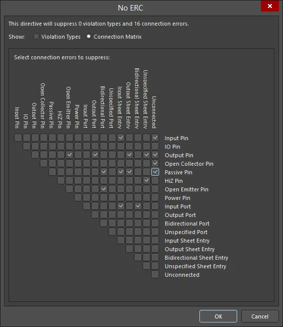
The No ERC dialog showing Violation Types mode (the first image) and Connection Matrix mode (the second image)
可通过在 Properties 面板的 Suppressed Violations 区域中(处于 No ERC mode,如上所述)单击 Specific Violations 来访问该对话框。

Options and Controls of the No ERC Dialog
-
Top statement - 此说明可让你快速查看当前抑制了多少种违规类型与连接错误。该说明会在你在对话框中进行更改时更新。
-
Show - 选择 Violation Types 或 Connection Matrix 以查看并配置相应的 No ERC 指令。
违规类型
此模式允许你抑制或取消抑制违规类型。
-
Violation Type To Suppress - 显示可配置的违规类型列表。
-
Report Mode - 显示所列违规类型的当前报告模式。
-
Suppress - 勾选复选框以抑制相应违规类型;取消勾选以取消抑制。
右键菜单
以下右键菜单命令中的 [xxx] 会根据右键时所选(或光标悬停)的违规类型而变化。
你也可以在某个 Violations Associated with 条目上右键,以访问针对整个对象的右键菜单命令。
-
Suppress only "[xxx]" - 用于仅抑制引号内列出的那些违规类型。
-
Unsuppress only "[xxx]" - 用于仅取消抑制引号内列出的那些违规类型。
-
Suppress All "[xxx]" - 用于抑制引号内所列对象的所有违规类型。
-
Unsuppress All "[xxx]" - 用于取消抑制引号内所列对象的所有违规类型。
-
Suppress All - 用于抑制所有列出的违规类型,不受对象或光标位置影响。
-
Unsuppress All - 用于取消抑制所有列出的违规类型,不受对象或光标位置影响。
-
Toggle All - 用于切换所有违规类型的 Suppress 复选框状态。
连接矩阵
此模式允许你抑制或取消抑制连接错误。
-
Grid - 使用网格中的复选框来抑制(勾选)或取消抑制(不勾选)所需的连接错误。
当光标悬停在某个复选框上时,该复选框及对应连接会以粗体高亮显示,从而更便于更新所需的连接错误。
右键菜单
以下右键菜单命令中的 [xxx] 会根据右键时所选(或光标悬停)的连接错误而变化。
-
Suppress only "[xxx]" - 用于仅抑制引号内列出的那些连接错误。
-
Unsuppress only "[xxx]" - 用于仅取消抑制引号内列出的那些连接错误。
-
Suppress All "[xxx]" - 用于抑制引号内的所有连接错误。此类命令有两个,连接的每一部分各一个。
-
Unsuppress All "[xxx]" - 用于取消抑制引号内的所有连接错误。 此类命令有两个,连接的每一部分各一个。
-
Suppress All - 用于抑制网格中的所有连接错误。
-
Unsuppress All - 用于取消抑制网格中的所有连接错误。
-
Toggle All - 用于切换所有连接错误的复选框状态。已勾选的将取消勾选;未勾选的将被勾选。
Specific No ERC 指令可配置为针对多个违规项,以支持会产生多个错误/警告的电路。
-
通过 SCH List 和 SCH Filter 面板。 List 面板允许你以表格形式显示来自一个或多个文档的设计对象,从而快速检查并修改对象属性。结合适当的过滤(使用相应的 Filter 面板 或 Find Similar Objects dialog)后,它可以仅显示落在活动过滤器范围内的对象——从而让你以更高的准确性与效率定位并编辑多个设计对象。

通用(Generic)No ERC 指令可以快速切换为特定(Specific)No ERC 指令,反之亦然:可通过 Properties 面板(在 Suppressed Violations 部分)进行切换,或在 SCH List 面板上切换 Suppress Specific Violations 属性。
停用 No ERC 指令
与其删除 No ERC 指令,不如将其设为非活动状态(在校验时视为禁用)。可通过切换该指令的 Active 属性来改变此状态——可通过任意一种编辑方法进行设置。处于非活动状态的 No ERC 指令在设计空间中将显示为灰色。

如果你需要临时停止使用某个 No ERC 指令,请将其设为非活动,而不是删除它。
控制 No ERC 指令的打印
默认情况下,打印时会包含 No ERC 标记。若要控制这一点——可以完全禁用其包含,或仅排除特定符号——请使用如下所示的 Print dialog。

在 Print dialog 中控制 No ERC 标记的打印。
No ERC
 使用 No ERC 标记来抑制关于电路中某个特定节点的错误/警告消息。
概述
No ERC 对象是一种设计指令。它放置在电路中的某个节点上,用于抑制在编译原理图工程时检测到并报告的所有电气规则检查(ERC)警告和/或错误违规条件。使用 No ERC 可以在你明确知道电路某处会产生警告(例如未连接引脚)时,有意限制该处的错误检查,同时仍对电路其余部分执行全面检查。
No ERC 指令支持多种不同样式,并可显示为任意颜色。可利用这一能力来体现该电路节点处的设计意图。
选择最能反映其在该电路位置功能的 No ERC 样式。
No ERC 指令有两种类型:
-
All Violations – 抑制所有可能的警告和/或错误条件。
-
Specific Violations – 仅抑制所选的警告或错误条件;其他任何警告或错误仍会被检测并报告。
可用性
No ERC 设计指令仅可在 Schematic Editor 中放置。要放置 No ERC 指令:
-
从主菜单点击 Place » Directives » Generic No ERC ,放置一个预配置为针对所有违规的 No ERC 标记。这有时也称为通用(Generic)No ERC 指令。
-
在原理图编辑器中右键,然后点击 Place » Directives » Generic No ERC。
放置 - 通用 No ERC 指令
启动命令后,光标将变为十字准星并进入放置模式。按以下步骤放置 No ERC 指令:
-
将光标移到导线或其他网络对象上,然后点击 Enter ,在电路该点放置指令。
-
继续放置更多 No ERC 指令,或右键/按 Esc 退出放置模式。
放置过程中还可执行的附加操作包括:
虽然可在放置过程中修改属性(通过
Tab 访问
Properties panel),但请注意:除非在
Preferences dialog 的
Schematic – Defaults 页面启用了
Permanent 选项,否则这些修改将成为后续放置对象的默认设置。启用该选项后,所做更改仅影响正在放置的对象以及同一次放置会话中后续放置的对象。
图形化编辑
No ERC 标记无法进行除位置更改之外的图形化修改。要移动 No ERC 标记,点击并按住拖动到新位置即可。
如果尝试对启用了 Locked 属性的对象进行图形化修改,将弹出对话框要求确认是否继续编辑。如果在 Preferences dialog 的 Schematic – Graphical Editing 页面启用了 Protect Locked Objects 选项,并且该设计对象的 Locked 选项也已启用,则该对象将无法被选择或进行图形化编辑。点击被锁定的对象以选中它,然后在 List panel 中禁用 Locked 属性,或禁用 Protect Locked Objects 选项,以便对对象进行图形化编辑。
非图形化编辑
提供以下非图形化编辑方法。
通过 No ERC 对话框或 Properties 面板编辑
Panel page: No ERC Properties
此编辑方法使用关联的 No ERC 对话框以及 Properties panel 模式来修改对象属性。

 No ERC dialog(第一张图)与 Properties 面板的 No ERC 模式(第二张图)
放置后,可通过以下方式打开 No ERC dialog:
-
双击已放置的 No ERC 对象。
-
将光标移到 No ERC 对象上,右键并从上下文菜单选择 Properties。
放置过程中,可按 Tab 键访问 Properties panel 的 No ERC 模式。No ERC 放置完成后,将显示所有选项。
放置后,可通过以下方式之一访问 Properties panel 的 No ERC 模式:
-
如果 Properties panel 已处于活动状态,选中 No ERC 对象即可。
-
选中 No ERC 对象后,通过工作区右下角的 Panels button 选择 Properties panel,或从主菜单选择 View » Panels » Properties。
如果在
Preferences dialog 的
Schematic - Graphical Editing page 上禁用了
Double Click Runs Interactive Properties 选项(默认),当双击该图元或在选中图元后右键并选择
Properties 时,将打开对话框。启用
Double Click Runs Interactive Properties 选项后,将打开
Properties panel。
尽管对话框与面板中的选项相同,但选项的顺序与布局可能略有不同。
通过关联的属性对话框编辑
此编辑方法使用 No ERC dialog 来修改特定(Specific)No ERC 对象的违规类型与连接错误。
与 Connection Matrix mode(第二张图)")
 No Erc dialog 显示 Violation Types mode(第一张图)与 Connection Matrix mode(第二张图)
可在 No ERC dialog 的 Suppressed Violations region 中,以及 Properties panel 的 No ERC mode 中点击 Specific Violations 来打开该对话框。
Specific No ERC 指令可配置为针对多个违规,以支持会产生多个错误/警告的电路。
编辑多个对象
Properties panel 支持多对象编辑:可修改当前所选对象中相同的属性设置。当手动选择多个相同对象类型,或通过 Find Similar Objects dialog,或通过 SCH Filter 或 SCH List panel 进行选择时,Properties panel 中未显示为星号(*)的字段项可对所有选中对象进行编辑。

通过列表面板编辑
Panel pages: SCH List、 SCH Filter
List panel 允许以表格形式显示一个或多个文档中的设计对象,从而快速检查并修改对象属性。结合适当的过滤(使用相应的 Filter panel 或 Find Similar Objects dialog),可仅显示落在活动过滤器范围内的对象——从而更准确、更高效地定位并编辑多个设计对象。
No ERC Properties
Schematic Editor 对象属性是可定义的选项,用于指定已放置对象的视觉样式、内容与行为。每种对象类型的属性设置通过两种不同方式定义:
-
Pre-placement settings – 大多数 No ERC 对象属性(或可合理预先定义的属性)可在 Preferences dialog 的 Schematic - Defaults 页面中作为可编辑的默认设置提供(通过设计空间右上角的
 button 进入)。在 Primitive List 中选择该对象,即可在右侧显示其选项。

-
Post-placement settings – 当在设计空间中选中已放置的 No ERC 时,所有 No ERC 对象属性都可在 No ERC dialog 和 Properties panel 中进行编辑。

如果在
Preferences dialog 的
Schematic - Graphical Editing page 中禁用
Double Click Runs Interactive Properties 选项(默认),当双击该图元,或在选中的图元上右键并选择
Properties 时,将打开该对话框。当启用
Double Click Runs Interactive Properties 选项时,将打开
Properties p
anel。
虽然对话框和面板中的选项相同,但选项的顺序和位置可能会略有不同。
在下面的属性列表中,默认情况下在 Preferences dialog 中不可用的选项会标注为“Properties panel only”。
位置 (Properties panel only)
-
(X/Y)
-
X (第一个字段)- 对象参考点相对于当前设计空间原点的当前 X(水平)坐标。编辑以更改对象的 X 位置。数值可用公制或英制输入;当输入的单位不是当前默认单位时,请在数值中包含单位。
-
Y (第二个字段)- 对象参考点相对于当前原点的当前 Y(垂直)坐标。编辑以更改对象的 Y 位置。数值可用公制或英制输入;当输入的单位不是当前默认单位时,请在数值中包含单位。
-
Rotation - 使用下拉列表选择旋转角度。
属性
-
Color - 单击彩色方框以打开下拉列表,从中选择默认颜色。
-
Symbol - 使用下拉列表从可用选项中选择默认值。
-
Active - 启用以使该图元处于活动状态。
抑制的违规项 (Properties panel only)
-
All Violations - 选择以显示该对象的所有违规项。违规项的 Violation Type 和 Report Mode 会显示在网格中。
-
Specific Violations - 选择以显示该对象的特定违规项。违规项的 Violation Type 和 Report Mode 会显示在网格中。
-
Add - 单击以打开 No ERC 对话框来添加新的违规项。单击 OK 后,新违规项将添加到网格中。单击
 以移除当前选中的违规项。
PCB 设计违规类型
与总线相关的违规项
Bus indices out of range
当连接到总线的组成网络的索引超出与该总线关联的网络所指定的范围时,会发生此违规。
消息面板中的通知
在 Messages 面板中会按以下格式显示通知:
Bus index out of range on <NetPrefix> Index = <NetIndex>
其中:
-
NetPrefix 是连接到总线的组成网络的前缀(例如, A 对于网络 A8,其连接到与网络 A[0..7] 关联的总线).
-
NetIndex 是该组成网络的错误索引(例如,网络 A8 的索引为 8)。
解决建议
将违规网络的索引修改为正确范围内,或直接重命名该网络。如果该网络是误命名且并非总线对象所传输网络的组成部分,通常会采用后者。
Bus range syntax errors
当与总线关联的网络语法指定不正确时,会发生此违规。
消息面板中的通知
在 Messages 面板中会按以下格式显示通知:
Bus range syntax error <NetName> at <Location>
其中:
-
NetName 是与违规总线对象关联的父网络名称。
-
Location 是违规总线对象电气热点的 X、Y 坐标。
解决建议
正确定义违规网络标识符(例如网络标号、端口、页入口等)的总线语法。正确语法应为以下格式之一:
-
NetName[LowerIndex..UpperIndex]
-
NetName[UpperIndex..LowerIndex]
例如,考虑一条承载两个组成网络 A0 和 A1 的总线。在这种情况下,总线语法应为 A[0..1] 或 A[1..0]。错误语法示例包括:A[0.1]、A[1-0]、A[0,1]、A[..1] 和 A[0..]。
Illegal bus range values
当与总线关联的网络语法中至少有一个索引为负值时,会发生此违规。
消息面板中的通知
在 Messages 面板中会按以下格式显示通知:
Illegal bus range value <BusLabel> at <Location>
其中:
-
BusLabel 是检测到非法值的已定义总线标注。
-
Location 是违规总线对象电气热点的 X、Y 坐标。
解决建议
正确定义违规网络标识符(例如网络标号、端口、页入口等)的总线语法。正确语法应为以下格式之一:
-
<NetName>[<LowerIndex>..<UpperIndex>]
-
<NetName>[<UpperIndex>..<LowerIndex>]
LowerIndex 且 UpperIndex 可以为 0 或正整数,但不能为负值。
Mismatched bus label ordering
当与同一总线切片关联的两个网络标识符所定义的总线标号排序方向不一致(升序或降序不一致)时,会发生此违规。
消息面板中的通知
在 Messages 面板中会按以下格式显示通知:
Mismatched bus ordering on <NetName> Low value first and High value first
其中:
-
NetName 是与不匹配总线排序相关联的父网络名称。
解决建议
找出总线排序不一致的网络标识符(端口、网络标号、页入口等)。确定正确的排序方向,并修改错误对象的命名。
Mismatched bus widths
当与同一总线切片关联的两个网络标识符所定义的总线标号宽度不同,会发生此违规。例如,名称为 A[0..7] 的端口可能连接到一条总线,而该总线所附的网络标号被定义为 A[0..15]。
消息面板中的通知
在 Messages 面板中会按以下格式显示通知:
Mismatched bus widths on bus section <NetName> (<BusSize1> and <BusSize2>)
其中:
-
NetName 是与不匹配总线对象相关联的父网络名称。
-
BusSize1 是第一个违规总线对象的宽度。
-
BusSize2 是第二个违规总线对象的宽度。
解决建议
找出总线标号宽度不一致的网络标识符(端口、网络标号、页入口等)。确定正确的宽度,并修改错误对象的命名。
Mismatched Bus/Wire object on Wire/Bus
当导线对象错误地连接到总线,或总线对象错误地连接到导线时,会发生此违规。例如,端口 A 可能连接到一条总线,但端口名称中未输入正确的总线标号语法(例如 A[0..1])。实际上,该端口是单一信号(或导线)对象,却被错误地连接到了总线。
消息面板中的通知
在 Messages 面板中会按以下格式显示通知:
<ObjectIdentifier> at <Location> placed on a <ObjectType>
其中:
-
ObjectIdentifier 表示不匹配的对象,可能是总线或导线对象(例如引脚、端口、电源端口、网络标号、跨页连接器、页入口)。该标识符将以下两种格式之一显示:
-
对于总线 –
Bus <Object> <Name>(例如 Bus Net Label GND_BUS[..])。
-
对于导线 –
Wire <Object> <Name>(例如 Wire Port TXD)。
-
Location 是该对象电气热点的 X、Y 坐标。
-
ObjectType 是违规对象所放置在其上的对象 – 可能是导线或总线。
解决建议
为解决该问题,请考虑以下几点:
-
Is the connection correct? – 连接到该对象的是否确实应为总线(或导线),反之亦然?
-
Is the object defined correctly? – 对于总线对象,确保对象名称使用正确的总线语法,形式为
<Name>[<LowIndex>..<HighIndex>] 或 <Name>[<HighIndex>..<LowIndex>]。例如,一个字节宽的数据输出端口可指定为 DAT_OUT[7..0]。对于导线对象,确保对象名称定义的是单一信号,且不要使用总线语法来定义。
Mixed generic and numeric bus labeling
当连接到同一总线切片的两个网络标识符(端口、网络标号、页入口等)在总线语法上不一致时,会发生此违规——一个以数字格式定义总线范围(例如 A[0..2]),另一个以通用格式定义范围(例如 A[0..b])。
消息面板中的通知
在 Messages 面板中会按以下格式显示通知:
Mismatched generic and numeric bus labeling on <NetName> <Level> value first and Generic
其中:
-
NetName是与总线标注不匹配相关联的父网络名称。
-
Level取决于该网络的数字排序方式。如果为升序(例如 [0..2]),则 Level 将显示为 Low。如果为降序(例如 [2..0]),则 Level 将显示为 High。
解决建议
确定哪些违规对象在其总线标注规范上存在错误,并据此进行修改。
不支持在总线名称中使用泛型(Generics)。请确保改用数值。
与元件相关的违规
Component has been deleted
当项目设计中至少有一个元件被删除时,会出现此违规。删除采用“软删除”方式:被删除的元件会被移动到专用的 Trash 位置,在那里可以通过(Restore)进行恢复,或通过浏览器界面中已删除条目的菜单选项(⋯)将其彻底移除(Permanently Delete),该浏览器界面属于 connected Workspace。
Messages 面板中的通知
在 Messages 面板中会按以下格式显示通知:
ComponentName: Component has been deleted
其中:
-
ComponentName是 Workspace 元件的名称。
解决建议
如果元件是误删的,具有相应访问权限的人员可在 Workspace 浏览器界面的 Trash 页面中将其恢复。否则,请将设计中使用的该元件替换为另一个等效元件,并确保该元件在已连接的 Workspace 中is 可用。
Component Implementations with invalid pin mappings
在编译集成库包(*.LibPkg)时,如果发现原理图元件与其链接模型之间的引脚映射无效,就会出现此违规。
Messages 面板中的通知
在 Messages 面板中会按以下格式显示通知:
ComponentName: Could not find port <ModelPinNumber> on model <ModelName> for pin <ComponentPinNumber> – 与 PCB 模型相关
ComponentName: Could not map port <ModelPinNumber> on model <ModelName> to a pin – 与仿真模型相关
其中:
-
ComponentName是源原理图库中元件的名称。
-
ModelPinNumber是期望的引脚/焊盘标号,但在链接模型上找不到。
-
ModelName是链接到该元件的模型名称。
-
ComponentPinNumber是源原理图元件上的引脚标号,模型中错误的引脚被映射到该引脚。
解决建议
解决方法是访问原理图符号与目标域模型之间的映射。为此,首先需要查看相应原理图库元件的属性。在 SCH Library panel 的 Components 列表中双击该元件条目,以打开 Properties panel,并加载该元件的属性。
如果显示的是与 PCB 模型相关的违规消息,请在面板的 Footprint 区域中选择该模型,然后点击列表下方的  按钮以打开 PCB Model dialog。进入后,点击 Pin Map 按钮以打开 Model Map dialog。在 Component Pin Designator 列中找到消息标记的引脚号(
ComponentPinNumber)。之所以产生违规,是因为 Model Pin Designator 列中的对应条目指向了 PCB 模型中不存在的焊盘标号。请按需修改该条目。通常应为一一对应映射,两侧标号相同。
如果显示的是与仿真模型相关的消息,请在面板的 Models 区域中选择该模型,然后点击列表下方的 按钮以打开 Sim Model dialog。进入后,点击 Port Map 选项卡。当模型引脚未正确映射到原理图元件的某个引脚时,就会出现此违规。这可能发生在模型引脚的条目被设置为一个已被映射的引脚,或设置为 Not Connected 的情况下。请按需修改该条目。
Component revision has inapplicable state
当检测到至少一个已放置的元件条目修订版(Component Item Revision)——从 connected Workspace 放置——处于不适用状态时,会出现此违规。例如,该元件当前处于 Depracated 或 Obsolete 状态,因此不应出现在最新的设计迭代中。适用性通过 State Properties dialog 中的 Allowed to be used in designs 选项来确定。在 Edit Lifecycle Definitions dialog 中,可通过双击父生命周期定义中该状态的条目,或选中条目并点击出现的编辑图标( )来打开该对话框以设置所需状态。当启用该选项时,处于该状态的 Item Revision 允许在设计中使用,视为 Applicable。当禁用该选项时,处于该状态的 Item Revision 不能被有效使用,视为 Inapplicable(或不适用)。
Edit Lifecycle Definitions dialog 可从
Preferences dialog 的
Data Management – Servers page 进入:点击你当前已登录的 Workspace 对应的
Properties 按钮,然后从下拉菜单中选择
Lifecycles。
Messages 面板中的通知
在 Messages 面板中会按以下格式显示通知:
Component <Designator> <Comment>: Component revision has inapplicable state
其中:
-
Designator是该元件实例的 Designator。
-
Comment是该元件实例的 Comment。
解决建议
使用 Item Manager dialog 选择一个可在设计中有效使用的替代 Component Item Revision。对每个处于不适用状态的元件都执行此操作。或者,你也可以在单个元件层级,将现有的 Component Item Revision 切换为不同的修订版,或切换为不同 Component Item 的修订版。在原理图中选中该元件,通过 Properties panel 访问其属性。在面板的 Properties 区域中,点击 Update 按钮以使用当前 Component Item 的最新修订版,或点击 Design Item ID 字段右侧的  按钮以访问你的 Workspace,并浏览选择另一个要使用的 Component Item Revision。
使用 Properties panel 或 Item Manager dialog 中提供的控件,选择该 Item 的更高修订版,且该修订版is处于适用状态;如果无法做到(该 Item 总体上不用于设计),则选择另一个 Item 的适用修订版。
注意
-
如果已放置的元件与其源 Workspace 失去连接——例如放置该元件的 Workspace 断开连接,或你已从 Workspace 退出登录——则会违反 Component revision has inapplicable state 检查。这会在 Messages panel 中体现为如下形式的条目:Component <Designator> <Comment>: Can't perform revision status validation: Failed to get session: Access denied! User login required for this service.
-
你也可以在设计发布流程中捕获在设计内被无效使用的元件。将 Component State Checking 添加并配置到你的整体发布验证方案中。
Component revision is Out of Date
当检测到从 connected Workspace 放置的元件已过期(不是最新修订版)时,会出现此违规。
Messages 面板中的通知
在 Messages 面板中会按以下格式显示通知:
Component <Designator> at <Location>: Component revision is Out of Date
其中:
-
Designator是该元件实例的 Designator。
-
Location是标记该违规元件实例原点的 X、Y 坐标。
解决建议
使用 Item Manager dialog 识别并更新不是最新修订版的元件。Item Manager 包含一个 Revision Status 列;对于任何不是最新修订版的元件,其状态将为 Out of Date。选中过期元件,右键并从菜单中选择 Update to latest revision。完成后,Generate 一个 ECO 以将这些更改应用到受影响的原理图。
或者,你也可以在单个元件层级,将现有的 Component Item Revision 切换为最新修订版。只需在原理图中选中该元件,通过 Properties panel 访问其属性。在面板的 Properties 区域中,点击 Update 按钮以使用当前 Component Item 的最新修订版。
注意
如果已放置的元件与其源 Workspace 失去连接——例如放置该元件的 Workspace 断开连接,或你已从 Workspace 退出登录——则会违反 Component revision is Out of Date 检查。这会在 Messages 面板中体现为如下形式的条目:Component <Designator> <Comment>: Can't perform revision status validation: Failed to get session: Access denied! User login required for this service.
包含重复子部件的元件
当在原理图设计中,同一个多分部件元件实例的相同部件被放置了不止一次时,就会发生此违规。例如,你放置了一个74HC32元件,其标号为U9,但不小心放置了该元件的第 1 部件的两个实例,导致设计中出现两个U9A实例。
Messages 面板中的通知
在Messages面板中会按以下格式显示一条通知:
Component <ComponentName> has duplicate sub-parts at <Location1> and <Location2>
其中:
-
ComponentName为违规元件的名称(由其标号与库引用构成)。
-
Location1为该特定子部件第一个实例的 X、Y 坐标。
-
Location2为该特定子部件重复实例的 X、Y 坐标。
解决建议
根据需要更改违规部件的分部件编号,可使用Increment Part Number命令——可从主Edit菜单或Part Actions子菜单(在元件上右键时)中访问。从Edit菜单启动该命令的优势在于你会保持在递增模式,从而可以循环切换分部件编号,直到到达所需编号。
具有重复引脚的元件
当一个元件中有两个或更多引脚具有相同的标号时,就会发生此违规。
Messages 面板中的通知
在Messages面板中会按以下格式显示一条通知:
Duplicate pins in component Pin <Identifier1> and Pin <Identifier2>
其中:
-
Identifier1为重复引脚的第一个实例的标识符,以“部件标号-引脚标号”的配对形式表示
-
Identifier2为重复引脚的第二个实例的标识符,同样以“部件标号-引脚标号”的配对形式表示。
解决建议
相应地更改违规引脚的标号,使每个引脚都具有唯一分配。对于已经放置的元件,其引脚标号可在原理图编辑器中编辑:
通常,重复问题会存在于库元件中;在这种情况下,你应在源原理图库中编辑该元件的引脚标号,然后使用Update From Libraries(Schematic Editor)或Update Schematics(Schematic Library Editor)命令将更改传递到已放置的元件实例。这两个命令分别可从相应编辑器的主Tools菜单中获得。
注
对于每个不同的元件,在Messages面板中只会列出一个违规实例。一个元件很可能有两个以上引脚使用相同标号,但当你通过面板的Details区域调查该违规时,只会列出前两个重复引脚(按引脚名称字母顺序)。
重复的部件标号
当设计中源原理图页之间至少有两个部件关联了相同的标号时,就会发生此违规。
Messages 面板中的通知
在Messages面板中会按以下格式显示一条通知:
Duplicate Component Designators <PartDesignator>
其中:
解决建议
按需为重复项分配不同且唯一的标号。可通过编辑每个违规标号来手动完成,或使用Annotate 对话框(Tools » Annotation » Annotate Schematics)。
或者,先使用Tools » Annotation » Reset Duplicate Schematic Designators命令重置重复的元件标号,然后使用Tools » Annotation » Annotate Schematics Quietly命令进行标注,而无需启动Annotate 对话框。
通用元件
当最终设计中包含Generic Component时,就会发生此违规。通用元件可在无需从可用元件来源中查找并选择特定制造商器件的情况下快速放置到设计中,作为占位符使用,便于后续替换为合适的元件。
Messages 面板中的通知
在Messages面板中会按以下格式显示一条通知:
Generic Component <PartDesignator> is placed at <Location>
其中:
-
Designator为已放置的通用元件实例的Designator。
-
Location为标记该违规通用元件实例原点的 X、Y 坐标。
解决建议
当设计推进到可以用具体的物理元件替换通用元件时,你可以在Properties面板的Design Item ID field中选择省略号菜单来使用Replace Component 对话框。注意,也可以从Item Manager或通过项目的ActiveBOM document完成此操作。
隐藏引脚连接不匹配
在多分部件元件中,如果一个对多个子部件通用的隐藏引脚连接到了不同的网络,就会发生此违规。
Messages 面板中的通知
在Messages面板中会按以下格式显示一条通知:
Mismatched hidden pin connections in Pin <Identifier> and Pin <Identifier>
其中:
-
Identifier用于标识相关引脚。该标识符以PhysicalComponentName-PinDesignator格式显示(例如:U2-7)。
解决建议
将违规引脚重新分配到正确的网络。通过在相应List 面板(SCHLIB List面板或SCH List面板)显示引脚属性时,在Hidden Net Name字段中输入网络名称,可将隐藏引脚分配到某个网络。如果在SCH List面板中进行此操作,请在面板中右键并启用Show Children选项,以在面板中列出引脚。
引脚可见性不匹配
此违规与多分部件元件的电源引脚(VCC 和 GND)有关。通常,这些引脚与第 0 部件关联,会自动连接到设计的 VCC 与 GND 网络,并且是隐藏的。如果你对某个元件部件启用了此类引脚的可见性,则它将不再连接到目标电源网络,并会被标记为错误。
Messages 面板中的通知
在Messages面板中会按以下格式显示一条通知:
Pin is visible in one sub-part and hidden in another sub-part
解决建议
要么在设计空间中禁用违规电源引脚的显示;要么如果保留引脚显示,请确保相应地将 VCC 和/或 GND 电源端口对象连接到该引脚。
缺少元件模型
在编译集成库包(*.LibPkg)时,如果在源原理图库中找不到某个元件所链接的模型,就会发生此违规。
Messages 面板中的通知
当链接模型为封装模型或仿真模型时,会在Messages面板中按以下格式之一显示通知:
<ComponentName>: Could not find <ModelName>——当模型搜索范围为Any时。
<ComponentName>: Could not find <ModelName> in <LibraryName>——当模型搜索范围为Library Name时。
<ComponentName>: Could not find <ModelName> in <Path>——当模型搜索范围为Library Path时。
其中:
-
ComponentName为源原理图库中元件的名称。
-
ModelName为链接到源元件但未能找到的封装或仿真模型名称。
-
LibraryName为指定包含该链接模型的库文件名称。
-
Path为指定包含该链接模型的库文件的绝对路径。
当链接的模型为信号完整性模型时,消息会在 Messages 面板中按以下格式显示:
<ComponentName>: Could not find 'GenericEntity' in <Path>
其中:
-
ComponentName 为源原理图库中该元件的名称。
-
Path 为库/模型的绝对路径。
解决建议
当问题是链接的封装或仿真模型时
该问题通常由以下一种情况导致:
-
在定义模型链接时,模型名称指定错误。
-
链接的模型不在指定的库文件中。
-
包含该链接模型的库文件已被移动或删除。
解决此违规的首要入口是与所链接模型类型对应的设置对话框——PCB Model dialog 或 Sim Model 对话框。在每种情况下,请检查并确保:
-
要链接到的模型名称正确,并且
-
用于定位该模型所在库/模型文件的选项使用正确。
显示的错误消息格式取决于你在定位模型时启用的搜索范围,并且在追踪模型链接问题时会非常有帮助:
-
如果在指定路径中找不到模型(搜索范围:
Library path),请确保你指定的库/模型文件确实存在于该位置,同时检查库/模型文件,确认其中是否存在具有指定名称的模型。
-
如果在指定库/模型文件中找不到模型(搜索范围:
Library name),请确保该库/模型文件已添加到 Available Libraries 列表(Project Libraries、Installed Libraries、Project Search Paths)。同时检查库/模型文件,确认其包含与链接中指定名称相同的模型。
-
如果只是找不到模型(搜索范围:
Any),请确保已将一个库/模型文件(其中包含与链接中指定名称相同的模型)添加到 Available Libraries 列表。
当问题是链接的信号完整性模型时
这通常是因为未指定信号完整性模型的类型(例如二极管、IC)而导致,可在信号完整性模型的相关设置对话框中解决。最简单的访问方式是在查看所选元件属性时,通过 Properties panel 进入。检查面板 General 选项卡上的 Models 区域中是否使用了正确的模型,并在必要时进行修改。可使用 Add 和 按钮创建新模型(从列表中选择 Signal Integrity)或修改现有的信号完整性模型。这将打开 Signal Integrity Model 对话框,其中 Import Ibis 按钮允许从 Ibis 模型文件导入引脚模型。
你也可以通过单击 Add » Ibis model 并使用随后出现的 Ibis Model 对话框来定义到模型及文件的链接,从而直接添加 Ibis 模型。
Missing pin found in component display mode
当在某个器件的某一种显示模式中检测到缺失引脚时,会发生此违规。
Messages 面板中的通知
通知会在 Messages 面板中按以下格式显示:
<NumberOfMissingPins> missing pins in <DisplayMode> of design item <DesignItemID>
其中:
-
NumberOfMissingPins 为在该器件中发现的缺失引脚数量。
-
DisplayMode 为发现缺失引脚的该器件的具体图形表示模式。一个器件具有 Normal 模式,并且最多可定义 255 个 Alternate 模式。
-
DesignItemID 为违规器件的 Design Item ID 属性。
解决建议
该违规通常出现在为元件定义了备用图形模式,但未将 Normal 模式中指定的所有引脚都在 Alternate 模式中指定(即不同图形显示模式之间必须具有相同数量的引脚)。
在源原理图库中,将缺失的引脚从现有显示模式复制到该元件的违规显示模式中。此操作也可以直接在已放置到原理图页上的器件上执行,但通常建议在库中解决问题,然后将更改推送过去(Tools » Update Schematics)。
Sheet Symbol with duplicate entries
当一个 Sheet Symbol 包含两个名称相同的 sheet entry 时,会发生此违规。
Messages 面板中的通知
通知会在 Messages 面板中按以下格式显示:
Sheet Symbol with duplicate entries Sheet Entry <Identifier> at <Location1> and <Location2>
其中:
-
Identifier 用于表示违规的 sheet entry。该标识符以 SheetSymbolName-SheetEntryName(SheetEntryIOType) 的格式显示。
-
Location1 为第一个违规 sheet entry 的 X、Y 坐标。
-
Location2 为第二个违规 sheet entry 的 X、Y 坐标。
解决建议
按需更改违规 sheet entry 对象的名称:可直接就地编辑名称,或双击违规 sheet entry,并在 Properties panel 的 Properties 区域中编辑其 Name(该面板会显示所选 sheet entry 的所有属性)。
也可以在浏览所选父级 sheet symbol 的属性时,从
Properties panel 的
General 选项卡上的
Sheet Entries 区域编辑 sheet entry 名称。
Sheet Symbols with duplicated indexes
在 multi-channel design 中,当两个或多个引用同一子原理图页、且其 Designator 字段包含 Repeat 关键字的 sheet symbol,其通道索引范围存在相同取值时,会发生此违规。
Messages 面板中的通知
通知会在 Messages 面板中按以下格式显示:
Sheet Symbols <ChannelIdentifier> have duplicated indexes: <ChannelIndexList>
其中:
-
ChannelIdentifier 为 sheet symbol 的 Designator 字段中使用的通道标识符。
-
ChannelIndexList 为在违规 sheet symbol 之间重复的通道索引列表(以逗号分隔)。
解决建议
更改违规 sheet symbol 对象的标号,使其索引范围不再有相同取值:可就地编辑 designator,或双击违规 sheet symbol,并在 Properties panel 的 Properties 区域中编辑其 Designator(该面板会显示所选 sheet symbol 的所有属性)。
Un-Designated parts requiring annotation
当设计中的某个元件被发现使用默认标号(带 ? 后缀)时,会发生此违规,即该元件尚未进行注释(annotation),或其标号已被重置。
Messages 面板中的通知
通知会在 Messages 面板中按以下格式显示:
Un-Designated Part <PartDesignator>
其中
-
PartDesignator 为未标号器件的默认标号(例如 U?、D?、C? 等)。
解决建议
按需为违规元件分配一个唯一的标号。可通过编辑标号手动完成,或使用 Annotate dialog(Tools » Annotation » Annotate Schematics)。
或者,使用 Tools » Annotation » Annotate Schematics Quietly 命令 在不打开 Annotate dialog 的情况下进行注释。
注意
对于每一种不同的标号类型(U?、D?、C? 等),在 Messages 面板中只会列出一个错误实例。实际可能存在多个错误。
Unused sub-part in component
当一个多分部件元件实例中的某个分部件未在设计中使用时,会发生此违规。例如,一个 74HC32 元件实例的四个分部件中,可能已有三个被放置并完成连线,但第四个未放置。
如果某个不包含任何图元(primitives)的分部件未放置到原理图中,则不会触发此违规(前提是在原理图符号编辑器中编辑该符号时,在 SCH Library 面板可见的符号分部件列表中,不含图元的分部件被列在所有含图元分部件的下方)。
Messages 面板中的通知
通知会在 Messages 面板中按以下格式显示:
Component <Identifier> has unused sub-part(s) (<PartNumber>)
其中
-
Identifier 为父级元件,使用 Designator Library Reference 的格式表示(例如 U11 74HC32)
-
PartNumber 为整数,用于指示未被使用的具体分部件(例如 1 表示分部件 A,2 表示分部件 B,依此类推)。
解决建议
放置未使用的分部件,并将其输入端连接到地。为确保使用相同的根标号,可复制该元件实例的一个已存在分部件;粘贴后,将其分部件编号相应递增。
与文档相关的违规
Ambiguous Device Sheet Path Resolution
当在多个已声明的 device sheet 文件夹中都找到了目标 device sheet(该目标在 Sheet Symbol 的 File Name 字段中指定)时,会发生此违规。
Messages 面板中的通知
通知会在 Messages 面板中按以下格式显示:
Ambiguous Device Sheet Resolution for <DeviceSheetName>
其中:
-
DeviceSheetName是父器件页(Device Sheet)符号的 File Name 字段中的当前条目。与 File Name 字段中的条目不同,该消息还包含扩展名(*.SchDoc)。
解决建议
使用 Messages 面板的 Details 区域,交叉定位到相关的器件页符号。双击该符号,通过 Properties panel 访问其属性。在 Source 部分的 General 选项卡中,会显示当前正在使用的器件页实例的完整路径。
请记住,所使用的器件页实例将是跨已声明的器件页文件夹中“第一个被检测到的”实例;并且这些文件夹(在 Preferences 对话框的 Data Management – Device Sheets page 中声明)会按从上到下的顺序进行搜索。如果当前使用的器件页就是正确实例,你可以直接忽略此违规项。否则,选择正确实例所在的文件夹,并点击 Move Up 按钮,直到该文件夹位于列表顶部。
但请注意,虽然这可能解决该特定器件页的即时问题,但歧义仍然存在。要彻底解决此问题,请找出冗余的器件页,并将其从其他已声明的器件页文件夹中移除。
Circular Document Dependency
当从 Design 主菜单使用 Create Sheet Symbol From Sheet 命令后,在 Choose Document to Place 对话框中选择了一个已作为项目子文档的原理图文档,并且所选原理图文档之间存在相互的 Device Sheet 链接时,会出现此违规项。
Messages 面板中的通知
在 Messages 面板中会按以下格式显示通知:
Circular dependency between document <DocumentName1> and document <DocumentName2>
其中:
-
DocumentName1DocumentName2 是两个彼此之间具有 Device Sheet 链接的文档名称。
解决建议
查看错误消息中列出的原理图文档,并修复它们之间的 Device Sheet 链接。
Missing child sheet for sheet symbol
当页符号与目标原理图子文档之间的链接无效时,会出现此违规项。可能发生在以下情况:
-
手动放置了页符号,但未在该符号的 File Name 字段中输入下一级文档引用。
-
在符号的 File Name 字段中错误输入了文档引用——实际上指向了一个不存在的文档。
-
被引用的目标文档已从项目中移除或被删除。
Messages 面板中的通知
在 Messages 面板中会按以下格式显示通知:
Missing child-sheet in <SymbolFileName> in Symbol <SymbolDesignator>
其中:
-
SymbolFileName 是父页符号的 File Name 字段中的当前条目。
-
SymbolDesignator 是父页符号的标号(designator)。
解决建议
当在设计空间中选中页符号时,在 Properties panel 的 General 选项卡的 Properties 部分中检查页符号的 File Name 字段条目。目标文档本身在 Source 部分(同一选项卡)中指定;对于标准页符号,其 Source 设为 Local。如果所需目标文档已存在,请确保在该字段中正确输入文档名(包括扩展名)。如果目标文档已从项目中移除且你仍可访问它,请将其重新添加回项目。如果目标文档不存在,请右键单击该符号,并从 Sheet Symbol Actions 子菜单中选择 Create Sheet From Symbol 命令。
注意
当放置了器件页符号(Device Sheet Symbol)但找不到目标器件页时,也会生成此错误。目标文档本身在 Properties panel 的 General 选项卡的 Source 部分中指定(在设计空间中选中器件页符号时);对于器件页符号,其 Source 设为 Device。
Multiple Top-Level Documents
在层次化设计中,当结构顶层存在两张或更多原理图页时,会出现此违规项。
Messages 面板中的通知
在 Messages 面板中会按以下格式显示通知:
Multiple top level documents: <SheetName> has been used
其中:
-
SheetName 是当前被用作顶层页的原理图文档名称。
解决建议
此问题通常是由于真正的顶层原理图上的页符号未正确指向预期的子页而引起。要解决此问题,先确定哪张原理图页是预期的子页。检查在顶层原理图上是否已为该预期子页放置页符号:
-
如果不存在页符号,请创建它——可手动放置,或使用主菜单中的 Design » Create Sheet Symbol From Sheet 命令。
-
如果页符号已存在,请确保它引用了该子页。当在设计空间中选中页符号时,在 Properties panel 的 General 选项卡的 Properties 部分中检查页符号的 File Name 字段条目。目标文档本身在 Source 部分(同一选项卡)中指定;对于标准页符号,其 Source 设为 Local。
Port not linked to parent sheet symbol
当子页上的端口未与父页符号上的页入口(sheet entry)匹配时,会出现此违规项。父页符号中的所有页入口都必须与子页上的对应端口同步(匹配)。
Messages 面板中的通知
在 Messages 面板中会按以下格式显示通知:
Port <PortName> not matched to Sheet-Entry at <Location>
其中:
-
PortName 是子页上端口的名称。
-
Location 是该端口电气热点的 X、Y 坐标。
解决建议
此问题可能由多种原因引起:
-
该端口对应的页入口不存在。
-
该端口对应的页入口存在,但名称不同。
-
该端口对应的页入口存在,但 I/O 类型不同。
对相关端口使用 Ctrl+Double Click 以上溯到父页符号。右键单击该页符号,并从出现的菜单中选择 Sheet Symbol Actions » Synchronize Sheet Entries and Ports。这将打开该页符号的 Synchronize Ports To Sheet Entries dialog。
使用该对话框将相关端口与所需页入口进行匹配。如果页入口不存在,可直接在对话框中创建。如果页入口存在但 Name 和/或 I/O Type 不同,你可以在匹配过程中决定要使用的 Name 和 I/O Type 来自端口还是页入口。
注意事项
当页入口与端口都存在但 Name 和/或 I/O Type 不同时,会有相应错误消息提示该页入口未与端口匹配。将页入口与端口同步后,这两个错误都会被清除。
Sheet Entry not linked to child sheet
当页入口未与父页符号所引用的子页上的端口匹配时,会出现此违规项。父页符号中的所有页入口都必须与子页上的对应端口同步(匹配)。
Messages 面板中的通知
在 Messages 面板中会按以下格式显示通知:
Sheet-Entry <SheetEntryName> not matched to Port at <Location>
其中:
-
SheetEntryName 是与父页符号关联的页入口名称。
-
Location 是该页入口电气热点的 X、Y 坐标。
解决建议
此问题可能由多种原因引起:
-
该页入口对应的端口不存在。
-
该页入口对应的端口存在,但名称不同。
-
该页入口对应的端口存在,但 I/O 类型不同。
右键单击作为相关页入口父对象的父页符号,然后从出现的菜单中选择 Sheet Symbol Actions » Synchronize Sheet Entries and Ports。这将使你能够访问该页符号的 Synchronize Ports To Sheet Entries dialog。
使用该对话框将相关页入口与所需端口进行匹配。如果端口不存在,可直接在对话框中创建。如果端口存在但 Name 和/或 I/O Type 不同,你可以在匹配过程中决定要使用的 Name 和 I/O Type 来自页入口还是端口。
注意
当页入口与端口都存在但 Name 和/或 I/O Type 不同时,会有相应错误消息提示该端口未与页入口匹配。将页入口与端口同步后,这两个错误都会被清除。
Sheet Names Clash
当项目在不同文件夹中包含多个同名的原理图文档时,会发生此违规。
Messages 面板中的通知
会在 Messages 面板中按以下格式显示一条通知:
Project <ProjectName> contains several documents named <SchematicDocumentName>
其中:
-
ProjectName 是与该错误相关联的项目名称。
-
SchematicDocumentName 是与项目中其他原理图文档同名的原理图文档。
解决建议
将有问题的原理图文档另存为不同的名称。
与 Harness 相关的违规
Conflicting Harness Definition
当同一 Harness Type 的 Harness Entry 存在冲突(无论是在图形层面还是文本层面,即在 Harness Definition File 中)时,会发生此违规。
Messages 面板中的通知
会在 Messages 面板中按以下格式显示一条通知:
Conflicting Harness Definition for <HarnessType>
其中:
-
HarnessType 是当前发生冲突的 Harness Type。
解决建议
更新 Harness Definition File 以反映更改,或删除有问题的 Harness Entry,或更改有问题的 Harness Entry 的 Harness Type。
该设计的 Harness Definition Files 可在该项目的
Settings\Harness Definitions Files 文件夹中找到,位置在
Projects 面板内。
Harness Connector Type Syntax Error
当 Harness Type 包含无效字符(例如 [ ] { } . : )或 Harness Type 为空时,会发生此违规。
Messages 面板中的通知
会在 Messages 面板中显示一条通知。
如果 Harness Type 含有无效字符,将按以下格式显示该消息:
Harness Connector Type <HarnessType> should not contain these characters [] {}. :
其中:
-
HarnessType 是当前发生冲突的 Harness Type。
如果 Harness Type 为空,将按以下格式显示该消息:
Harness Connector Type cannot be Blank
解决建议
选中有问题的 Harness Connector 后,在 Properties 面板的 Properties 部分中指定一个有效的 Harness Type。确保该条目不包含无效字符。
Invalid Connection to a Harness Connector
当导线、总线或信号 Harness 终止于 Harness Connector 内部,或连接到 Harness Connector 的边缘,但未连接到 Harness Entry 时,会发生此违规。
Messages 面板中的通知
会在 Messages 面板中按以下格式显示一条通知:
<ObjectType> (<Location1> To <Location2>) ends inside Harness Connector <HarnessType> but it is not connected to any of its Harness Entries
其中:
-
ObjectType 是有问题对象的类型——Net(用于导线)、Bus 或 Signal Harness。
-
Location1 是有问题对象起点的 X、Y 坐标。
-
Location2 是有问题对象终点的 X、Y 坐标。
-
HarnessType 是有问题的 Harness Connector 的 Harness Type。
解决建议
确保导线、总线或信号 Harness 连接到该 Harness Connector 的某个 Harness Entry;或编辑导线/总线/信号 Harness,使其不在 Harness Connector 内部终止,且不连接到 Harness Connector 的边缘。
Missing Harness Type on Harness
当连接 Sheet Entries 的 Signal Harness,或连接 Sheet Entry 与 Port 的 Signal Harness 缺少 Harness Type 时,会发生此违规。
Messages 面板中的通知
会在 Messages 面板中按以下格式显示一条通知:
Missing Harness Type on Signal Harness
解决建议
在 Signal Harness 上为以下对象中的至少一个指定 Harness Type:
Multiple Harness Types on Harness
当在一条 Signal Harness 上定义了多个 Harness Type 时,会发生此违规。
Messages 面板中的通知
会在 Messages 面板中按以下格式显示一条通知:
Multiple harness types on harness <HarnessType1>, <HarnessType2>
其中:
-
HarnessType1 和 HarnessType2 是在该 Signal Harness 上指定的多个 Harness Type。
解决建议
在该 Signal Harness 上仅指定一个 Harness Type:
Unconnected Harness Entry
当没有导线、总线或信号 Harness 连接到 Harness Entry 时,会发生此违规。
Messages 面板中的通知
会在 Messages 面板中按以下格式显示一条通知:
Unconnected Harness Entry <Identifier>
其中:
-
Identifier 用于标识相关的 Harness Entry。该标识符以 HarnessType-HarnessName 的格式显示。
解决建议
确保有导线、总线或信号 Harness 连接到该 Harness Entry。
Unknown Harness Type
当发现某个 Harness Type,但在 Harness Definition file 中找不到匹配的定义时,会发生此违规。这可能由以下两种原因之一导致:
-
某条 Signal Harness 连接到了具有未知 Harness Type 的对象(Sheet Entry、Port 或 Harness Entry)。
-
当 Harness Definition file 中的某个 Harness Entry 引用了未知的 Harness Type。
Messages 面板中的通知
会在 Messages 面板中按以下格式显示一条通知:
Unknown Harness Type <HarnessType>
其中:
-
HarnessType 是当前未知的 Harness Type。
解决建议
确保 Sheet Entries、Ports 和 Harness Entries 具有已知的 Harness Type,并确保 Harness Definitions 准确无误:
与 Nets 相关的违规
Adding hidden net to sheet
当项目中有两个或更多隐藏引脚在其 Hidden Net Name 属性中输入了相同的值时,会发生此违规。隐藏引脚有时用于在多分部件中定义电源引脚。通常,当使用了带隐藏引脚的库元件且设计人员并未意识到这些隐藏引脚的存在时,就会出现此警告。
Messages 面板中的通知
会在 Messages 面板中按以下格式显示一条通知:
Adding hidden net
解决建议
当有问题的引脚满足以下属性时,就会产生该问题:
-
启用了 Hide 选项
-
Hidden Net Name 字段包含特定的电源网络名称
如果这是设计使然,则可以忽略该警告。或者,你可以在设计空间中启用这些引脚的显示。但该选项可能并不理想,尤其是当你有许多连接到电源网络的隐藏引脚时。在设计空间中显示这些引脚会造成杂乱,因为每个引脚都需要用导线连接到相应的电源端口对象——从而使原理图更难阅读。
如果你选择显示隐藏引脚,并且这些引脚被分配到 Part Zero,那么它们将出现在项目中放置的每个分部件上。对于未隐藏的多分部件电源引脚,更好的做法可能是在该元件中专门为电源引脚创建一个独立的分部件。
Hidden Net Name 字段只能在 SCHLIB List 面板或 SCH List 面板中访问。在处理多个对象时,在 List 面板中编辑其属性可能更高效。

注
在 Messages 面板中只会列出此类违规类型的一个实例。当使用面板的 Details 区域调查该错误时,将列出一个条目,用于反映正在添加的网络。可能会添加多个网络——例如 GND 和 VCC——但只会列出其中一个,并按字母顺序决定。如果你清除了某个特定网络的违规项,则下一个网络(按顺序)将会在此违规类型下显示。
Adding Items from hidden net to net
此违规与元件相关,当你将一个或多个引脚指定为隐藏,并连接到设计中现有的网络时就会发生——例如,将电源引脚连接到 VCC 或 GND。
Messages 面板中的通知
在 Messages 面板中会按以下格式显示通知:
Adding items to hidden net <NetName>
其中:
解决建议
当在相关的 Component Pin Editor dialog 中,违规引脚具有以下属性时,就会出现该问题:
此问题的解决需要按元件逐一处理,并且还取决于元件是否包含多个子部件。
对于非多分部件元件,请在设计空间中启用引脚显示(启用 Show 选项)。你需要将每个引脚连接到相应的电源端口,以连接到你希望的网络。
上述方案也可用于多分部件元件,但更好的方案是将 Part Number 字段设置为 0。保持该引脚的 Show 选项为禁用。对以这种方式连接到电源网络的每个引脚重复此操作。理想情况下,电源网络连接应通过源库元件中的部件 0 来分配。
Bus Object on a Harness
当信号线束中的 Port、Sheet Entry 或 Net Label 的名称采用 [X..Y] 这种形式(表示总线对象)时,会出现此违规。
Messages 面板中的通知
在 Messages 面板中会按以下格式显示通知:
Bus <Object> <ObjectName> at <Location> placed on a harness
其中:
-
Object 为违规的端口、页入口或网络标号。
-
ObjectName 为违规对象的名称。
-
Location 为违规对象的 X、Y 坐标。
解决建议
修改违规对象的名称,使其不使用总线语法。
Differential Pair Net Connection Polarity Inversed
当差分对网络的极性与其所连接的差分对引脚极性不一致时,会出现此违规。例如,正网络连接到了负引脚,或反之亦然。
Messages 面板中的通知
在 Messages 面板中会按以下格式显示通知:
Inversed connection on differential pair <PairName>: net <NetName> is connected to pin <PinDesignator> (<Polarity>)
其中:
-
PairName 为差分对名称(例如 V_TX1)。
-
NetName 为违规网络的名称(例如 V_TX1_P)。
-
PinDesignator 为违规网络所连接的器件引脚位号(例如 E6)。
-
Polarity 为该引脚的极性(例如 negative)。
解决建议
确保连接导线上的网络标号极性与所连接的差分对引脚极性一致。例如,如果引脚名为 IO_L02N_0 且网络标号为 V_TX1_P,请将网络标号改为 V_TX1_N。
如果出现一对此类型的违规消息——一条是该对的正网络接到了器件的负引脚,另一条是同一对的负网络接到了器件的正引脚——只需将所附的网络标号互换即可。
Differential Pair Net Unconnected To Differential Pair Pin
当差分对网络未连接到物理器件的差分对引脚时,会出现此违规。
Messages 面板中的通知
在 Messages 面板中会按以下格式显示通知:
Net <NetName> of differential pair <PairName> is not connected to a differential pair pin
其中:
-
NetName 为该对中正极性或负极性网络的名称(例如 V_RX1_N 或 V_RX1_P)。
-
PairName 为差分对名称(例如 V_RX1)。
解决建议
真正的差分对引脚在物理器件中是硬连线定义的(例如 Xilinx Virtex-II Pro FPGA 器件)。尽管此类引脚名称中可能包含标识符 N(负)或 P(正),但你不能仅通过更改引脚名称就把一个引脚变成差分引脚。
解决此类违规时请考虑以下情况:
-
如果差分对网络本身正确,但被连接/布线到了器件的错误引脚上,请确定正确引脚并相应移动网络标号。
-
如果差分对网络被错误地指定为差分对网络,请将相关网络标号改为正确的(非差分)命名,并移除连接导线上的差分对指令。
-
如果当前连接差分对网络的引脚实际上在设计中根本不使用,请确保移除网络标号、导线以及差分对指令,并在其上放置 No ERC 标记。
Differential Pair Unproperly Connected to Device
当差分对网络未正确连接到物理器件的差分对引脚时,会出现此违规。
Messages 面板中的通知
在 Messages 面板中会按以下格式显示通知:
Misconnected differential pair <PairName>: net <NetName> should be connected to pin <PinDesignator>
其中:
-
PairName 为差分对名称(例如 V_TX1)。
-
NetName 为该对中正极性或负极性网络的名称(例如 V_TX1_N 或 V_TX1_P)。
-
PinDesignator 为违规网络应连接到的器件引脚位号(例如 E6)。
解决建议
此类违规通常是因为差分对网络的导线对象未与器件的目标引脚形成电气连接。请确保网络导线与器件引脚本身正确连接。
Duplicate Nets
当在设计中检测到两个同名网络时,会出现此违规。
Messages 面板中的通知
在 Messages 面板中会按以下格式显示通知:
Duplicate Net Names <Object> <NetName>
其中:
-
Object 为 Wire 或 Bus Slice 或 Element[n](用于总线元素)之一。
-
NetName 为受影响网络的名称。
解决建议
在创建设计数据模型时,网络按以下方式创建:
-
在每个原理图页内,对每一组相互连接的电气对象创建一个唯一网络。
-
然后检查 Net Identifier Scope,以确定设计是扁平(flat)还是层次(hierarchical)。
-
如果设计是扁平的,则页级网络会在各个原理图页之间直接连接。
-
如果设计是层次结构:
-
通过连接到下层网络的 Port,从该 Port 向上到父页中 Sheet Symbol 上的 Sheet Entry 建立连通性,然后
-
在父页上于 Sheet Entry 与其他已连接的电气对象之间建立连通性。
要了解更多关于扁平与层次设计的信息,请参阅 Creating Circuit Connectivity in Your Schematics 页面。
例如,在以下情况下可能会出现此违规:
-
设计为扁平结构,但在设计中使用了端口。Net Identifier Scope 被自动(或手动)设置为
Flat (Only ports global)。如果在不同原理图页之间使用了相同的网络标号,就会发生违规。这是因为每个原理图页上定义的网络标号即使同名,也仍然只在该页内局部有效。此时的解决方法是确保不同原理图页之间使用唯一的网络标号。
-
扁平化后的原理图页之间的网络连续性被无意中使用了不同名称的端口或跨页连接器(off sheet connector)而打断。请沿网络追踪到每个原理图页的输入/输出端口,并确保这些端口名称一致。
- 在层次化设计的两个不同分支中,可能会使用同一个网络——也就是说,使用不同的图纸符号来引用不同的子图纸,但顶层图纸入口和下级端口使用了相同的名称,并且这两个符号之间通过实际的导线或总线相连。若不小心使用了名称不同的图纸入口,或遗漏了连接这些图纸入口的实际总线/导线,就可能导致这些分支之间的网络连续性被破坏。请确保连接两个图纸符号的实际导线已放置且连接正确,并且图纸入口的命名一致。
External and Schematic Net Names are Unsynchronized
当原理图 FPGA 元件某个引脚的网络名与外部源文件中该引脚的网络名不一致时,会出现此违规。
Messages 面板中的通知
会在 Messages 面板中按以下格式显示一条通知:
External <NetLabelName> and Schematic <NetLabelName> are Unsynchronized for Pin <xx>
其中:
-
NetLabelName 为违规的网络标号名称。
-
xx 为引脚编号。
解决建议
在 Pin Mapper 对话框中选中违规的引脚,在 Schematic 区域访问下拉解决方案选项,然后选择 Update Pin File( ),将网络名从原理图传输到外部 FPGA 引脚文件,然后再次验证工程。
Floating net labels
当检测到某个网络标号在设计中处于悬空状态(即 未附着在导线或总线对象上)时,会出现此违规。对于未与电路其余部分电气连接的总线电源端口对象,也会出现该消息。
Messages 面板中的通知
会在 Messages 面板中按以下格式显示一条通知:
Floating Net Label <NetLabelName>
其中:
解决建议
确保违规的网络标号对象已连接到所需的导线或总线对象。如果该网络标号是多余的,请将其从设计中删除。
同时检查导线/总线对象及其关联的网络标号是否在栅格上。对象可以手动移回栅格上,或使用 Edit » Align » Align To Grid 命令。
另外,检查导线是否确实是 really 导线,而不是线段对象!
Floating power objects
当检测到某个电源端口对象在设计中处于悬空状态——未与元件电气连接——时,会出现此违规。例如,可能已放置电源端口,但尚未将其接线到电路其余部分。
Messages 面板中的通知
会在 Messages 面板中按以下格式显示一条通知:
Floating Power Object <NetName>
其中:
-
NetName 为与该悬空电源端口对象关联的网络名称。
解决建议
确保违规的电源端口对象按需要连接到电路中。如果该电源端口是多余的,请将其从设计中删除。
注意
此消息与标准的单信号电源端口对象相关。
Global Power-Object scope changes
当基于端口的对象(端口、跨图连接器)连接到了电源端口对象时,会出现此违规。该电源对象将不再能以全局级别存在(连接到全局电源网络),而会被改为本地级别的电源网络。
Messages 面板中的通知
会在 Messages 面板中按以下格式显示一条通知:
Global Power-Object <NetName> at <Location1> has been reduced to local level by presence of port at <Location2>
其中:
-
NetName 为该电源端口对象所关联的网络。
-
Location1 为电源端口对象电气热点的 X、Y 坐标。
-
Location2 为端口对象电气热点的 X、Y 坐标。
解决建议
此违规通常发生在电源端口对象错误地接到了端口,而不是预期的引脚或图纸入口。不过,在某些情况下,你可能希望强制(并使用)这种范围变更。请评估端口与电源端口之间的连接是否符合预期;如果不符合,请移除电源端口,并按需要将剩余的端口对象接线到其预期目标。
Harness Object on a Bus
当端口、图纸入口或线束入口等对象关联了线束类型(表示连接到信号线束),但却接线到总线上时,会出现此违规。
Messages 面板中的通知
会在 Messages 面板中按以下格式显示一条通知:
Harness <Object> <ObjectName> at <Location> placed on bus
其中:
-
Object 为违规的端口、图纸入口或线束入口。
-
ObjectName 为违规对象的标注。
-
Location 为违规对象的 X、Y 坐标。
解决建议
确保违规对象(端口、图纸入口或线束入口)未连接到总线,而是连接到信号线束。
Harness Object on a Wire
当端口、图纸入口或线束入口等对象关联了线束类型(表示连接到信号线束),但该对象却连接到导线上时,会出现此违规。
Messages 面板中的通知
会在 Messages 面板中按以下格式显示一条通知:
Harness <Object> <ObjectName> at <Location> placed on wire
其中:
-
Object 为违规的端口、图纸入口或线束入口。
-
ObjectName 为违规对象的标注。
-
Location 为违规对象的 X、Y 坐标。
解决建议
确保违规对象(端口、图纸入口或线束入口)未连接到导线,而是连接到信号线束。
Missing Negative Net in Differential Pair
当在设计中某个差分对对象未检测到负极性网络时,会出现此违规。该差分对的正极性网络是存在的。
Messages 面板中的通知
会在 Messages 面板中按以下格式显示一条通知:
Missing Negative Net for differential pair <PairName>, positive net <NetName>
其中:
-
PairName 为已定义正极性网络的差分对名称(例如 V_RX1)。
-
NetName 为正极性网络名称(例如 V_RX1_P)。
解决建议
此违规通常出现在以下情况:
-
差分对指令未附着在该信号配对的负极性导线上。所需的网络标号(例如
V_RX1_N)已按要求附着在导线上。
-
未将命名正确的网络标号(例如
V_RX1_N)附着在该信号配对的负极性导线上。所需的差分对指令已按要求附着在导线上。
要解决此违规,请定位该差分对的负线导线对象,并确保网络标号与差分对指令都已附着,且网络标号名称按要求指定。负线的网络标号与正线基本相同,但后缀应为 _N 而不是 _P。或者,如果负线导线对象连接到了命名正确的端口对象,则可在 Project Options dialog 的 Options 选项卡上启用 Allow Ports to Name Nets 选项,而无需在导线上附加网络标号。
在 Project Options 对话框的 Options 选项卡中,你还可以添加自定义差分对后缀,以定义自定义的差分对命名方案。
Missing Positive Net in Differential Pair
当在设计中某个差分对对象未检测到正极性网络时,会出现此违规。该差分对的负极性网络是存在的。
Messages 面板中的通知
会在 Messages 面板中按以下格式显示一条通知:
Missing Positive Net for differential pair <PairName>, negative net <NetName>
其中:
-
PairName 为已定义正极性网络的差分对名称(例如 V_RX1)。
-
NetName 为负极性网络名称(例如 V_RX1_N)。
解决建议
此违规通常出现在以下情况:
-
差分对指令未附着在该信号配对的正极性导线上。所需的网络标号(例如
V_RX1_P)已按要求附着在导线上。
-
未将命名正确的网络标号(例如
V_RX1_P)附着在该信号配对的正极性导线上。所需的差分对指令已按要求附着在导线上。
为解决此违规,请找到该差分对中的正线(positive wire)对象,并确保网络标号(net label)和差分对指令(differential pair directive)都已附加到该对象上,同时按要求指定网络标号的名称。正线的网络标号应与负线的网络标号基本相同,但后缀使用 _P 而不是 _N。或者,如果正线对象连接到了一个已按规范命名的端口(port)对象,则可以在 Project Options 对话框的 Options 选项卡中启用 Allow Ports to Name Nets 选项,而无需在线上附加网络标号。
在 Project Options 对话框的 Options 选项卡中,你还可以添加自定义的差分对后缀,以定义自定义的差分对命名方案。
Net Parameters with no name
当参数集(parameter set)对象附加到网络对象(导线或总线)上,并且该参数集中至少有一个已定义参数未分配名称时,会发生此违规。
Messages 面板中的通知
通知会以如下格式显示在 Messages 面板中:
Invalid net-parameter name at <Location>
其中:
-
Location 是与该网络关联的参数集对象热点(hotspot)的 X、Y 坐标。
解决建议
在 Properties 面板中进入该违规参数集对象的 Parameter Set 模式,并确保其中定义的所有参数都已分配名称。如果违规的组成参数不需要,直接将其从参数集中移除即可。
Net Parameters with no value
当参数集对象附加到网络对象(导线或总线)上,并且该集合中至少有一个已定义的类(class)未分配值时,会发生此违规。
Messages 面板中的通知
通知会以如下格式显示在 Messages 面板中:
Invalid net-parameter value at <Location>
其中:
-
Location 是与该网络关联的参数集对象热点的 X、Y 坐标。
解决建议
在设计空间中选择违规的参数集对象,以在 Properties 面板中访问其属性。确保面板 Classes 区域中定义的所有参数都已分配值。如果违规的类参数不需要,将其从集合中移除。
如果该类参数在设计空间中可见,你可以直接为其输入值(单击一次选中,然后再次单击进入就地编辑),或选中它并打开
Properties 面板。然后在面板的
Properties 区域中使用
Value 字段为其输入值。
Nets containing floating input pins
当检测到设计中某个已放置器件的输入引脚处于悬空状态(即未与电路中任何其他部分电气连接)时,会发生此违规。
Messages 面板中的通知
通知会以如下格式显示在 Messages 面板中:
Net <NetName> contains floating input pins (<PinList>)
其中:
-
NetName 是违规网络的名称。
-
PinList 是该网络中处于悬空状态的引脚列表(以逗号分隔)。
解决建议
此类违规可能由多种情况引起。解决此类违规时,请考虑以下方面:
-
如果该引脚在设计中不使用,可将其连接到合适的电源线(例如
GND),或在其上放置 No ERC directive。
-
确保连接到该引脚的布线已形成电气接触,即导线或总线连接到了该引脚的电气热点。
-
使用 Navigator 面板追踪与该违规引脚相关的父网络(parent net)的连通性。有时,引脚“悬空”是因为网络的其他位置存在断点。例如,引脚可能从该页的输入端口接收信号,而该端口又由设计层级中更高层的链接 sheet entry 提供信号;但该 sheet entry 的输入可能已断开。修复该 sheet entry 的连接即可解决悬空输入引脚违规。
-
在 Messages 面板中查找与同一父网络相关的其他违规消息,尤其是提到未连接对象的消息。这有助于判断连通性断点所在位置。
Nets containing multiple similar objects
当检测到同一父网络中有两个或更多相同类型(引脚、端口、sheet entry)且电气 I/O 规格相同的对象彼此相连时,会发生此违规。例如,一个 Input Port 连接到一个 Input Port。
Messages 面板中的通知
通知会以如下格式显示在 Messages 面板中:
Net <NetName> contains multiple <ObjectType> (<ObjectList>)
其中:
-
NetName 是违规网络的名称。
-
ObjectType 是在违规网络中发现多个实例的对象类型。该条目也会反映对象的电气类型。
-
ObjectList 是在违规网络中发现的该对象所有实例列表(以逗号分隔)。
解决建议
判断这些被连接的违规对象是否会造成实际的连通性问题;若会,则相应地更改其中一个或两个对象的 I/O 规格。如果某个对象是冗余的,将其从设计中移除。如果某个对象原本应连接到设计的其他部分却接错了目标(因此成为错误网络的一部分),请确保将其从当前网络断开并连接到正确的网络。
说明
-
此类违规所使用的实际报告模式取决于具体对象类型、它们的电气 I/O 类型,以及在 Options for Project 对话框的 Connection Matrix 选项卡中定义的相应报告级别(Project » Project Options)。
-
Options for Project 对话框的 Error Reporting 选项卡中的 Report Mode 设置,不会影响 Messages 面板中此类违规所显示的 Report Mode 设置。但它会被用于设计空间内的在线(实时)错误报告。在线报告的控制项位于 Preferences 对话框的 Schematic – Compiler 页面。请注意,如果 Connection Matrix 中针对某个“对象类型 - I/O 类型”组合的单项检查被设置为
No Report,则不会出现该组合的在线错误报告。
Nets with multiple names
当检测到设计中的某个网络关联了多个名称时,会发生此违规。
Messages 面板中的通知
通知会以如下格式显示在 Messages 面板中:
Nets <Identifier> has multiple names (<NameList>)
其中:
-
Identifier 表示连接类型以及网络名称。连接可以是以下之一:
-
Wire – 标识符将以
Wire NetName 格式显示(例如 Wire DTSA)。
-
Bus – 标识符将以
Bus Slice NetName 格式显示(例如 Bus Slice A[0..7])。
-
Bus Element – 标识符将以
Element[n]: NetPrefix 格式显示(例如 Element[0]: A)。
-
NameList 是与违规网络关联的所有名称列表(以逗号分隔)。这些名称可能来自附加的网络标号、sheet entry、电源端口(power port)以及跨页连接器(off sheet connector)。
解决建议
可通过确保与某个网络关联的所有网络标识符名称一致来解决此违规。然而,在许多情况下,为同一网络使用不同名称是有益的——例如,当该网络出现在层级化设计的不同分支上,不同名称能更好地反映这些分支中传导的信号。同样,你可能希望用与连接到输入/输出导线或总线的网络标号不同的名称来描述某个 sheet symbol 的 sheet entry。
若要在设计中自由地为网络使用多个名称,并防止相关违规消息出现在 Messages 面板中,请在 Options for Project 对话框的 Error Reporting 选项卡中,将此违规类型的 Report Mode 设置为 No Report (Project » Project Options)。
Nets with no driving source
当检测到设计中的某个网络没有驱动源时,会发生此违规。也就是说,该网络不包含至少一个具有以下电气类型之一的引脚:
- IO
-
输出
-
开集电极
-
高阻态(HiZ)
-
开射极
-
电源
网络中不包含上述类型之一的引脚并不少见,例如在以下情况下可能发生:
-
某个网络从连接器引脚连接到输入引脚。
-
某个网络从串联无源器件(其引脚为无源类型)连接到输入引脚。
Messages 面板中的通知
会在 Messages 面板中按以下格式显示一条通知:
Net <NetName> has no driving source (<PinList>)
其中:
-
NetName为违规网络的名称。
-
PinList为该网络中引脚的逗号分隔列表。
解决建议
编辑连接器/无源器件的引脚,使其成为上述列出的电气类型之一。
Nets with only one pin
当某个器件引脚连接到了电气对象(例如导线或网络标号),表明该引脚属于某个网络,但该网络中没有其他引脚时,就会发生此违规。通常这是由于布线错误导致,或是某个未使用的器件引脚上连接了一小段导线。
Messages 面板中的通知
会在 Messages 面板中按以下格式显示一条通知:
Net <NetName> has only one pin (Pin <PinName>)
其中:
-
NetName为父网络的名称。
-
PinName为器件位号-引脚编号标识符。
解决建议
默认情况下,此消息不会出现在 Messages 面板中。如果你已启用对此违规类型的报告并希望解决该问题,请确保违规网络在设计中至少连接到两个器件引脚。
Nets with possible connection problems
当同一网络上彼此连接的两个对象具有不匹配的电气类型、可能导致连接问题时,就会发生此违规。此错误检查所考虑的对象类型组合可以是引脚、端口或页入口的任意组合。例如,一个 Output Port 连接到一个 Bidirectional Port。
Messages 面板中的通知
会在 Messages 面板中按以下格式显示一条通知:
<NetName> contains <ObjectType1> and <ObjectType2> objects (<Reference>)
其中:
-
NetName为包含可能冲突对象的父网络名称。
-
ObjectType1为第一个违规对象类型。
-
ObjectType2为第二个违规对象类型。
-
Reference为一个或两个对象的标识符(例如
Port PortName、 Pin PinName、 and Sheet EntrySheetSymbolName-SheetEntryName)。
解决建议
判断这些违规的已连接对象是否确实会造成连接问题;若会,则相应更改其中一个或两个对象的 I/O 规格。
备注
-
此类违规所使用的实际报告模式取决于具体对象类型、其电气 I/O 类型,以及在 Connection Matrix 选项卡(位于 Options for Project 对话框中,Project » Project Options)上定义的对应报告级别。
-
在 Error Reporting 选项卡(位于 Options for Project 对话框中)上的 Report Mode 设置,不会影响在 Messages 面板中针对该类违规显示的 Report Mode 设置。不过,它会被用于设计空间内的在线(实时)错误报告。在线报告的控制项位于 Preferences 对话框的 Schematic – Compiler 页面。请注意:如果在 Connection Matrix 中将某个特定“对象类型-I/O 类型”组合的单项检查设置为
No Report,则不会出现该组合的在线错误报告。


 AI 翻译
AI 翻译