
Defining Design Requirements Using the Constraint Manager

Altium Essentials: Schematic Updating
This content is part of the official Altium Professional Training Program. For full courses, materials and certification, visit Altium Training.
 ).
).The Constraint Manager is a document-based, spreadsheet-like user interface that allows you to view, create, and manage the design constraints used for your PCB designs.

Some of the advantages of using the Constraint Manager, especially for complex designs with many nets, classes, etc., are:
-
Availability at the project level that makes the access to the design constraint management similar from both schematic capture and PCB design domains.
-
A shift from query-based rule scoping to an applied object type matching simplifies constraint rule creation.
-
Use of constraint sets to expedite the process of defining the constraints.
-
Rule priority is automatic based on the natural hierarchy of design objects.
-
Using a document-based presentation interface rather than a dialog means that the schematic and PCB editor and its associated functions remain active and accessible.
Accessing the Constraint Manager
The Constraint Manager is accessed by selecting the Design » Constraint Manager command from the main menus of the schematic or PCB editor.

Access the Constraint Manager from the schematic editor

Access the Constraint Manager from the PCB editor

Constraint Types
Using the buttons at the top left of the Constraint Manager, you can switch between its views to define different constraint types.
![]()


Notes on working with the Constraint Manager:
-
Use the Units option in the Properties panel (or the corresponding options in the Tools » Measurement Units sub-menu in the main menus; shortcut:
Ctrl+Q) to switch between the measurement units (mm or mils) in which the values are shown in the Constraint Manager grid area. -
Use the Show Default Values option in the Properties panel (or the corresponding option in the View main menu or the View Options sub-menu of the grid area's right-click menu) to toggle the visibility of default values (e.g., values inherited from a net class or differential pair) in the Constraint Manager. When shown, these default values are displayed in the Constraint Manager grid area in grey. Custom values are displayed in the Constraint Manager grid area in white.
-
When in the Physical or Electrical view, use the Show Only Object Custom Values option in the Properties panel (or the corresponding option in the View main menu or the View Options sub-menu of the grid area's right-click menu) to toggle the visibility of object entries with the default values (effectively, to filter out entries with default values when the option is enabled).
-
Copying and pasting values from/to cells is supported – use the commands of the Copy/Paste Values sub-menu from the context menu or the
Ctrl+CandCtrl+Vshortcuts. -
Use the Search field at the top-right of the Constraint Manager to filter the list of objects by entering a search string. Click the
 icon at the right of the Search bar to remove the currently defined search string.
-
Use the Comment field at the bottom of the Constraint Manager when a cell for a constraint/rule is selected to add a comment to this constraint/rule, for example, a meaningful description of what it is being used for (
 ). When the lower part of the Constraint Manager allows defining constraints for different rules, you can define an individual comment to each of them by switching the current rule using the Rule drop-down (
 ).
).
-
A save action must be performed in the Constraint Manager before changes are reflected in the design. Use the File » Save (when the Constraint Manager is accessed from the schematic) or File » Save to PCB (when the Constraint Manager is accessed from the PCB) command from the main menus of the Constraint Manager or the
Ctrl+Sshortcut to do this. -
On first save of the Constraint Manager when accessed from the schematic side, the schematic constraints document (
Constraints.xml) is added to the project and made available through the Projects panel (in the Settings/Constraints sub-folder – ). In addition, constraints data in the document is reloaded/refreshed after updating the project from the connected Workspace.
-
If there are any changes in the schematic design or in the PCB layer stack (changes affected layers and/or impedance profiles), click the
 button at the top of the Constraint Manager (accessed from the respective editor) to reflect these changes in the Constraint Manager. Clicking this button also allows you to import directives from schematics to the Constraint Manager – learn more. If you have changes in the Constraint Manager not saved yet, a dialog that warns you that these changes will be lost appears for confirmation.
-
The following global options are available in the Clearances Settings region of the Properties panel from the Clearances and Physical views when the Constraint Manager is accessed from either the schematic or PCB:
-
Ignore Pad to Pad clearances within a footprint – use this option to apply the setting to all defined clearance rules. This option allows you to specify whether clearances between pads in the same component footprint are ignored.
-
Apply zero Keepout clearance – when this option is enabled, a default clearance rule is applied, with a gap of ‘0’, between a keepout and all other primitives in the design. Note that this rule is not visible on any of the Constraint Manager views and, therefore, cannot be modified. If disabled, the regular clearance matrix values will be followed.
-
-
You can quickly undo or redo changes made in the Constraint Manager by using
 in the upper left of the design space or using Edit » Undo/Redo from the main menus and is available in most areas including rules, scopes and constraint sets. As in other areas of the software, the icons/commands are only available if an action (for undo) or undo action (for redo) has been performed.
Working with the Clearance Matrix
By default, the clearance matrix in the Clearances view of the Constraint Manager includes a single All Net Classes to All Net Classes entry with which you can define a default clearance value between any nets in the design. Use the Add control at the top left of the matrix (or right-click any cell in the clearance matrix and use the Add command from the context menu) to show a pop-up with a list of currently defined net and differential pair classes. Select one or more required classes (multiple class entries can be selected using the Shift+Click or Ctrl+Click technique) and click the Add button. A row and a column for each selected class will be added to the matrix.
![]()
Click a cell where the row and column of two classes intersect to select it and show the detailed clearance settings at the lower part of the Constraint Manager, where you can define specific clearance values between different objects and on different layers.
![]()
Use the Clearance field in the lower part to enter the required value that will be applied to all object pairings and all layers for this class pair. Alternatively, double-click a cell in the matrix in the upper part to directly enter the required value.
Enter the required clearance values for specific object pairs in the table. Note that the cell in the clearance matrix shows the range of minimum and maximum values defined in the table.
![]()
Notes on working with the Clearances view:
-
Entering a value into a cell in the clearance matrix or into the Clearance field will automatically apply that value to all of the fields in the grid region in the lower part of the Constraint Manager when a cell in the clearance matrix is selected. You only need to edit in the grid region when you need to define a clearance based on the object type.
-
In the detailed clearance settings at the lower part of the Constraint Manager, you can also enable the Creepage constraint for the selected classes and define the creepage value (
 ). This constraint tests the creepage distance between the targeted signals across the board surface through unplated holes, cutouts, and around the board edge.
-
In the detailed clearance settings at the lower part of the Constraint Manager, you can also enable the Z-Axis Clearance constraint for the selected classes and define the Z-axis clearance value (
 ). This constraint is used to check the minimum clearances between primitives on different copper layers.
-
To reset the clearance value for a specific object pair (for example, a Track to Track pair) to its default (i.e., to the value defined for the All Net Classes to All Net Classes entry), select its cell in the bottom table and press the
Deletekey or right-click the cell and select the Reset to Default command from the context menu. -
To reset the clearance value for all object pairs of a specific entry in the clearance matrix (for example, a net class and another net class entry) to their defaults, right-click the corresponding cell in the clearance matrix and select the Remove Rule command from the context menu.
-
To remove a class from the clearance matrix, right-click any cell in the row for this class in the clearance matrix and select the Remove Scope command from the context menu.
 ).
).Configuring Clearances per Layer
Using the tabs below the table, you can also define clearance values by layers. Use the Add control to add a tab for a specific layer.
![]()
Filtering Classes
To leverage your work with a large number of classes in the Clearances view, you can use the filtering/grouping feature. This enables the construction of filters (or groupings) of classes to allow switching between, and working with, focused sub-sets of the clearance matrix.
Use the ![]() button at the top right of the Clearances view to access a pop-up from where you can create, edit, remove, and enable/disable filters.
button at the top right of the Clearances view to access a pop-up from where you can create, edit, remove, and enable/disable filters.
![]()
To create a new filter, click the ![]() button and then click the
button and then click the ![]() button in the pop-up that appears.
button in the pop-up that appears.
![]()
Define a unique name for the new filter, enable the required group of classes. Use the Search field to filter the list according to the entered search string and use the Reset control to quickly disable all enabled entries in the list. Once the required classes are selected, click ![]() .
.
![]()
With a filter created, use the available controls in the pop-up to enable, disable, edit, or remove it as needed. Use the Clear All control to quickly disable all enabled filters. Note that when at least one filter is enabled, the button at the top right is shown as ![]() .
.
Working with Physical and Electrical Constraints
When in the Physical or Electrical view of the Constraint Manager, click a cell in the grid area to show the settings of the corresponding rule(s) at the lower part of the Constraint Manager, where you can define their constraint values.
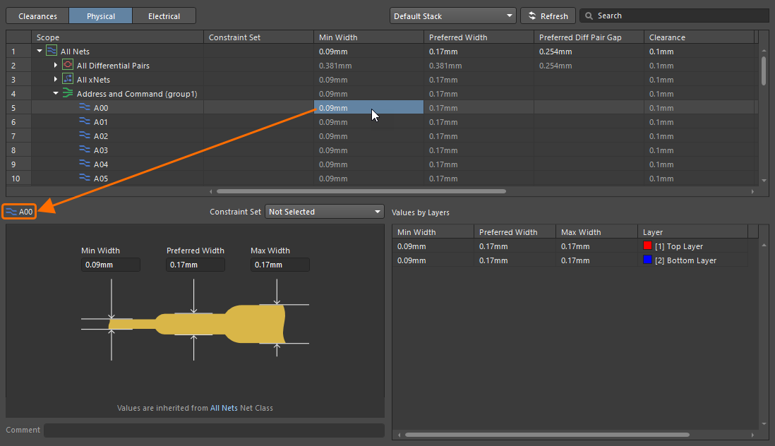
The following constraints can be configured in the Physical view:
-
Width – this constraint specifies the width of tracks placed on the signal layers.
-
Diff Pair Gap – this constraint specifies the clearance (or gap) between the nets in the scoped differential pair(s).
-
Clearance – this constraint specifies minimum clearance allowed between objects of the scoped net(s) and objects of other nets in the design.
-
Via Style – this constraint specifies the style of vias that can be used when routing. You can define specific Min/Max/Preferred values for the via's diameter and hole size (Min/Max Preferred) or, when the Constraint Manager is accessed from the PCB or when configuring constraints for a specific layer stack (learn more), use templates available to the board design (Templates).
-
Polygon Connect – this constraint specifies the style of the connection from a component pad, or routed via, to a polygon pour.
For more information about constraint values, refer to the Plane Rule Types page.
-
Same Net Clearance – this constraint specifies minimum clearance allowed between any two primitive objects belonging to the same net (e.g., between a via and pad on the same net, or two track segments in the same net).
-
Routing Neck Down – this constraint specifies the maximum allowed length of continuous routes whose width is between the Min Width and Preferred Width defined by the applicable Width constraint.
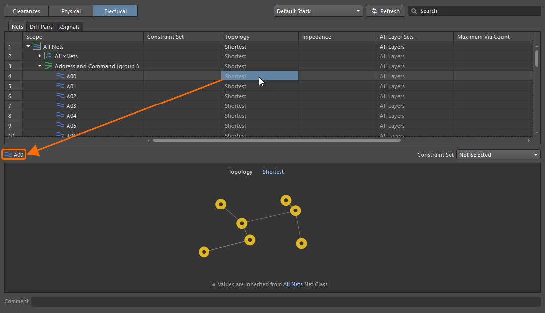
The following constraints can be configured in the Electrical view:
-
The Nets tab:
-
Topology – this constraint specifies the topology to be employed when routing nets on the board. The topology of a net is the arrangement or pattern of the pin-to-pin connections.
For more information about constraint values, refer to the Routing Rule Types page.
-
Impedance – this constraint specifies the minimum and maximum net impedance allowed.
-
All Layer Sets – this constraint specifies which layers are allowed to be used for routing.
-
Maximum Via Count – this constraint specifies the permitted maximum number of vias.
-
Min / Max Total Length – this constraint specifies the minimum and maximum lengths of a net.
-
Max Stub Length – this constraint specifies the maximum permissible stub length for a net with a daisy chain topology.
-
Max Via Stub Length – a stub is the length of via or pad barrel that protrudes beyond the last-used signal layer that the via/pad connects on. Back drilling will be applied to suitable vias/pads in the targeted nets, in accordance with the enabled side-of-board Layer checkboxes, and the back drill pairs defined on the Back Drills tab of the Layer Stack Manager.
For more information about constraint values, refer to the High Speed Rule Types page.
For more information about back drilling, refer to the Controlled Depth Drilling (Back Drilling) page.
-
-
The Diff Pairs tab:
-
Impedance – this constraint specifies the minimum and maximum net impedance allowed.
-
Gap – this constraint specifies the clearance (or gap) between the nets in the scoped differential pair(s).
-
Width – this constraint specifies the permissible width to be used for tracks when routing the differential pair.
-
Max Uncoupled Length – this constraint specifies the value for the maximum permissible uncoupled length between positive and negative nets within the differential pair.
-
Tolerance – this constraint specifies a length tolerance when comparing the longest net in the diff pair.
-
Dynamic Phase Tolerance – this constraint specifies the permissible phase mismatch between the tracks in a diff pair above which compensation is required.
-
Matching Distance – this constraint specifies the distance after exceeding the tolerance, for which compensation must be applied.
-
-
The xSignals tab:
-
Tolerance – this constraint specifies a length tolerance when comparing each xSignal within the xSignal class with the xSignal selected as the Matching Target for the class.
-
Notes on working with the Physical or Electrical views:
-
The Constraint Manager defines the priorities of the rules in these views automatically: the priority is ordered from All (lowest) to object class to object (highest).
-
To remove custom constraint values defined by a specific rule (effectively, reset values for this rule to its defaults), right-click the corresponding cell in the grid and select the Remove rule command from the context menu.
-
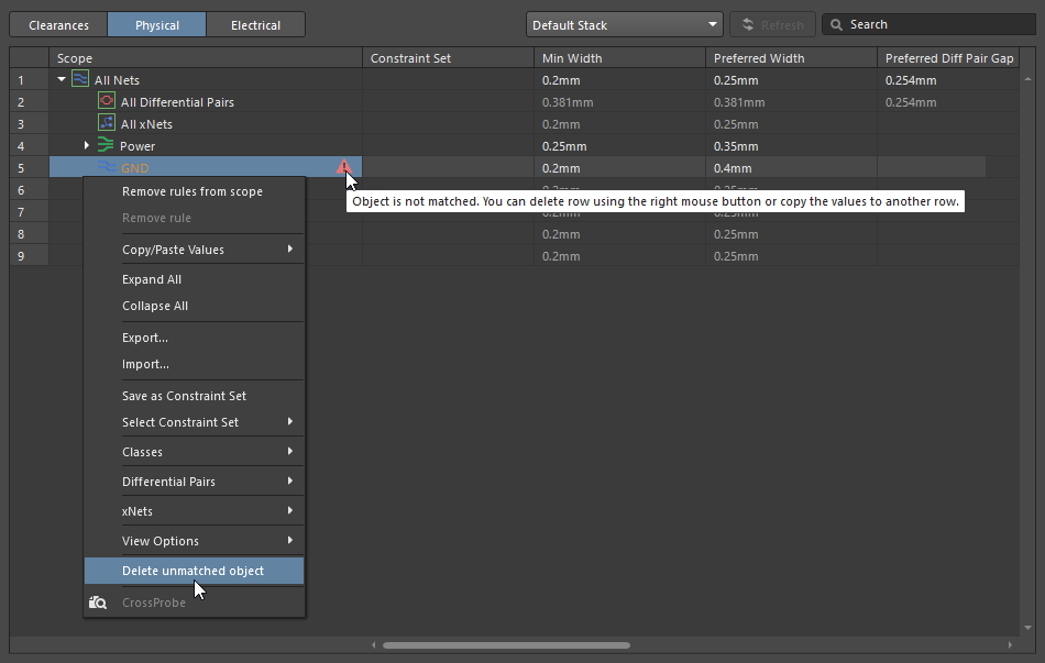
To remove custom constraint values by all rules for an object, right-click any cell in the row for this object in the grid and select the Remove rules from scope command from the context menu.
-
All nodes, except those predefined (e.g., All Nets), are collapsed in the Physical and Electrical views by default. You can use the Expand All and Collapse All right-click menu commands to control the grid nodes.
-
When a value is entered in the Physical view's top grid for a single net or xNet (Min Width or Preferred Width), differential pair (Min Width, Preferred Width, or Preferred Diff Pair Gap) or net/xNet/diff pair class, this value will be propagated to corresponding width (Min Width/Preferred Width/Max Width) or gap (Min Gap/Preferred Gap/Max Gap) fields in the constraint regions below. Note that an entered value will be propagated to other fields only if the object does not have the specific rule defined.
-
When defining values for the minimum, maximum, and preferred routing widths and differential pair gaps in the Physical view, the Values by Layer table at the bottom of the view will highlight invalid entries using red text. This could happen, for example, when you specify a minimum constraint value that is greater than the maximum constraint value. The incorrect constraint definition is further highlighted by the width/gap values becoming red in the top grid of the view.
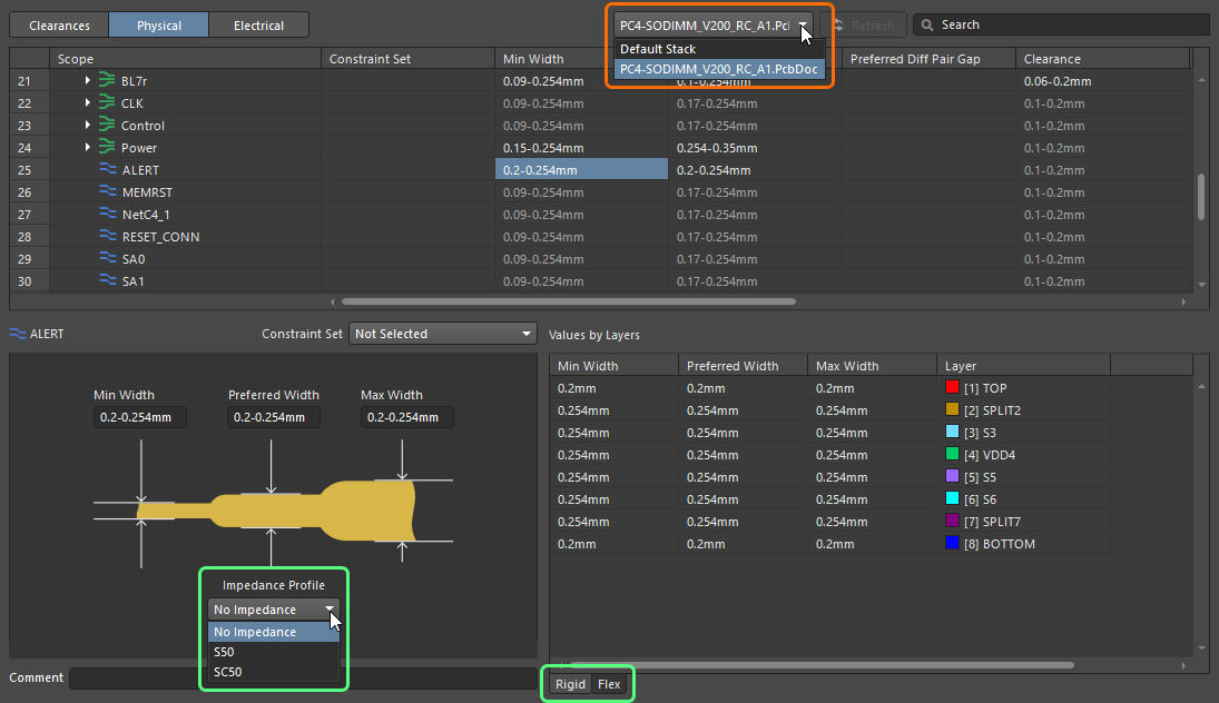
Configuring Constraint Values per Layer
When accessing the Constraint Manager from the schematic, you can configure the Width and Differential Pairs Routing constraints for layers in a chosen layer stack.
Using the drop-down at the top of the Constraint Manager, select an entry for a specific PCB document of the design project. If the selected PCB contains multiple layer stacks, you can choose the required stack for which constraints need to be configured using tabs in the lower part of the Constraint Manager when the corresponding rule is selected. Also, you can use a chosen Impedance Profile (where defined as part of the selected PCB’s layer stack).
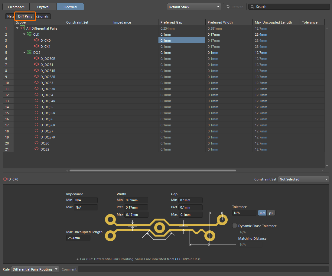
Defining Differential Pairs
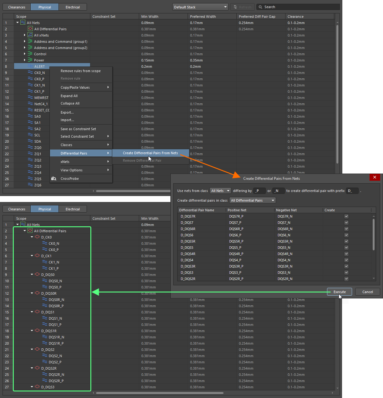
Differential pairs are created from the Physical view or from the Diff Pairs tab of the Electrical view of the Constraint Manager. For the Constraint Manager to create differential pairs from nets, the nets to be paired must have a consistent naming scheme (i.e., they have a common root followed by a consistent positive/negative suffix, for example, TX0_P and TX0_N).
Right-click anywhere in the grid area of the Physical view or the Diff Pairs tab of the Electrical view and select the Differential Pairs » Create Differential Pairs From Nets command from the context menu to open the Create Differential Pairs From Nets dialog to define differential pair creation options. The filters at the top of the dialog enable you to quickly target these nets in terms of the net class to which they belong and the particular differentiating factor that has been used to distinguish the positive and negative nets in an intended pairing, for example, _P and _N. You can also define a prefix to be added to the differential pair objects created and determine to which differential pair class they will be added.
For each differential pair object, the dialog lists its constituent positive and negative nets. By default, all prospective differential pair objects are selected for creation, and individual ones can be excluded by clearing the associated Create check box.
When all options are set as required, click the ![]() button – the differential pair objects will be created and shown in the Physical view of the Constraint Manager, with constituent nets listed under their entries.
button – the differential pair objects will be created and shown in the Physical view of the Constraint Manager, with constituent nets listed under their entries.
Differential pairs can also be created from xNets. Use the drop-down at the top of the Create Differential Pairs From Nets dialog to select All xNets or a specific xNet class. When other options in the dialog are configured as required, click the ![]() button to create differential pairs accordingly.
button to create differential pairs accordingly.

To remove a differential pair, right-click its entry and select the Differential Pairs » Remove Differential Pair command from the context menu. You can also remove multiple differential pairs by selecting their entries using the Ctrl+Click, Shift+Click, or Click, Hold&Drag technique, right-clicking the selection, and choosing the Differential Pairs » Remove Differential Pair command from the context menu.
The Diff Pairs tab of the Electrical view can also be used for explicitly managing differential pairs. A hierarchical list of the differential pairs in the design is shown on this tab. Select a cell for a differential pair or differential pair class to present constraints for it in the lower part of the Constraint Manager.
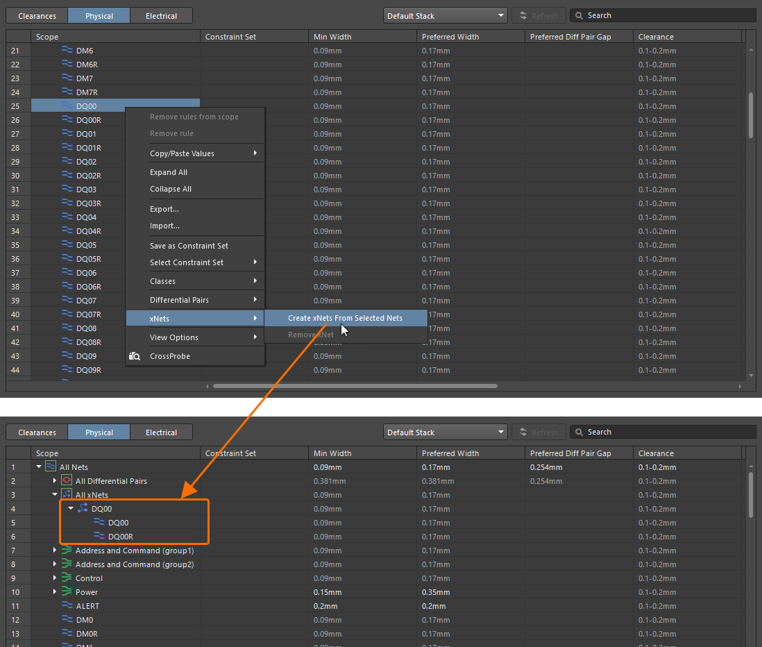
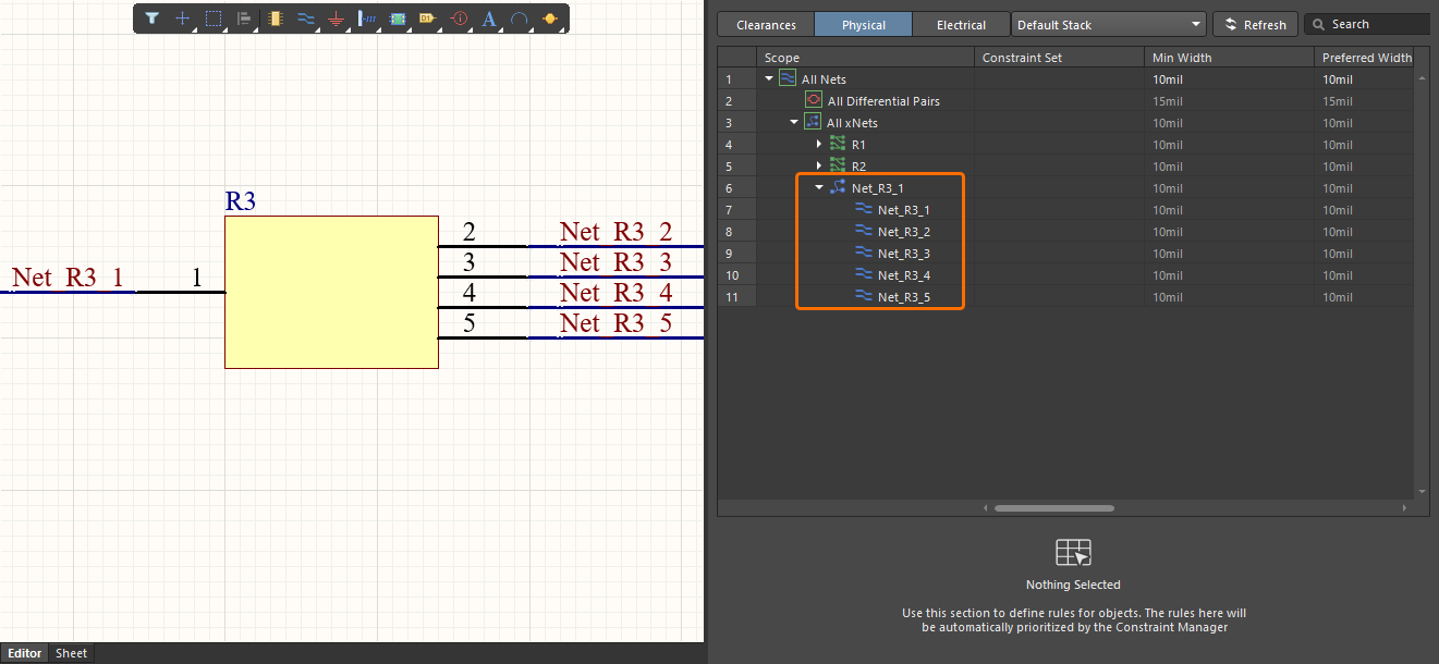
Defining xNets
A path from a source component to a destination component passing through one or more series components can be defined as an xNet.
Comma-separated lists of prefixes for designators of components that can be used as source or destination components (Sources/Destinations) and series components (Discretes) can be defined in the xNets Creation region of the Options tab of the Project Options dialog.

The xNets Creation region of the Options tab of the Project Options dialog
")
An example path that can be defined as an xNet in the Constraint Manager (according to the xNet creation settings shown above)
In the Physical or Electrical view of the Constraint Manager (when it is accessed from either a schematic or PCB), right-click a net to be included in a new xNet and select the xNets » Create xNets From Selected Nets command from the context menu. A new xNet will be created and shown in the Physical or Electrical views of the Constraint Manager, with constituent nets listed under its entry.
Generation of xNets also supports serial components with more than two pins. The following serial components are supported:
-
Dual-inline component with an even number of pins – xNets can be generated from nets connected to the first and the last pins of the component, then to the second and the second to last pins, etc. (
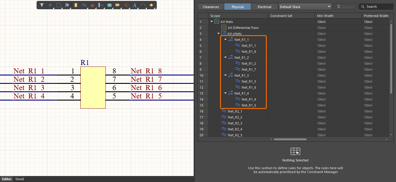 )
)
-
Single-inline component with an even number of pins – xNets can be generated from nets connected to the first and the second pins of the component, then to the third and the fourth pins, etc. (
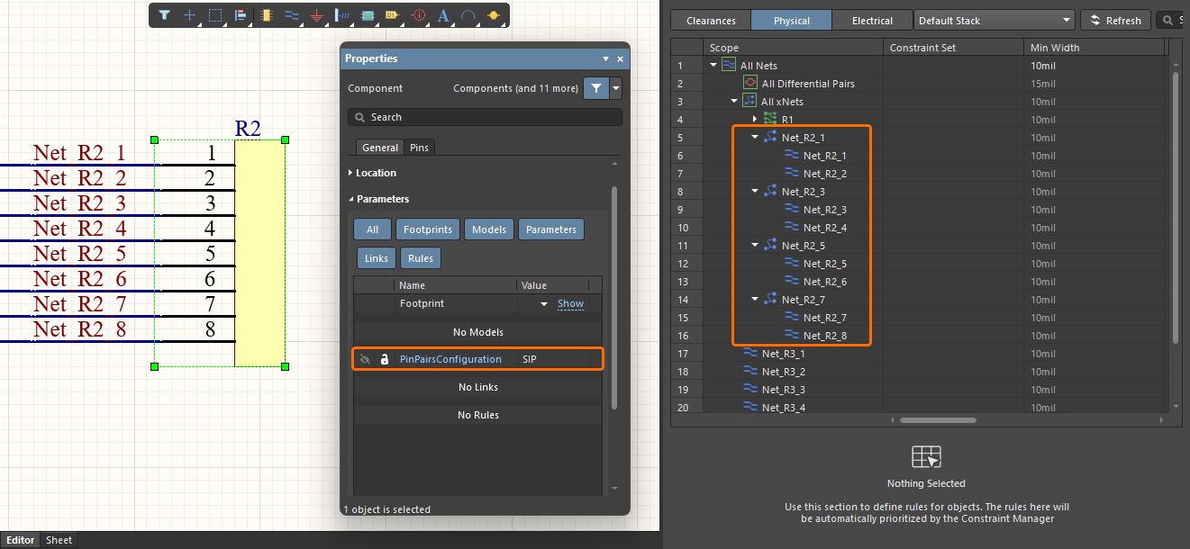 ) Note that the component must include a parameter named
 PinPairsConfigurationwith valueSIP; otherwise, xNets will be generated as in the case of the dual-inline component. -
Component with an odd number of pins – an xNet is generated from nets connected to all pins of the component. (
 )
)
To remove an xNet, right-click its entry and select the xNets » Remove xNet command from the context menu. You can also remove multiple xNets by selecting their entries using the Ctrl+Click, Shift+Click, or Click, Hold&Drag technique, right-clicking the selection, and choosing the xNets » Remove xNet command from the context menu.
Defining xSignals
From the Constraint Manager, you can also define xSignals – user-defined signal paths between two nodes in the PCB. When in the Electrical view of the Constraint Manager, select the cell in the Topology column for a net or xNet, choose Custom from the drop-down in the lower part of the Constraint Manager, and then use the provided controls to define the custom topology and select corresponding xSignals.
An example of defining xSignals for an xNet shown below is described and demonstrated thereafter.

An example of xNet for which xSignals should be created.
A custom topology can be defined using the topology graph in the lower part of the Constraint Manager. Use the right-click menu in the graph area to add and remove nodes and change their type from Source to Destination and back and Click, Hold&Drag the nodes to define the tolopogy.
The list of proposed xSignals (named using the <SourceNetName> (<SourcePinDesignator> → <DestinationPinDesignator>) scheme) appear at the right of the grid area. The list is divided into two groups: xSignals going from a source to a destination (S-T) and xSignals going from one destination to another (T-T). Use checkboxes for groups or individual xSignals to select/deselect xSignals to be created. Selected xSignals will appear on the xSignals tab of the Electrical view.
An example of creating xSignals using the topology graph
For a created xSignal class (refer to the Defining Classes section below for details), the Tolerance constraint can be defined, and an xSignal within this class can be selected as Matching Length. When the Constraint Manager is accessed from the PCB side, the Actual Value and Margin columns are also available.

In the PCB document, the defined xSignals can be browsed from the PCB panel in its xSignals mode. Also, corresponding From-Tos will be created and can be browsed from the PCB panel in its From-To Editor mode.


Defining Classes
The Constraint Manager allows you to define classes of nets, differential pairs, xNets, and xSignals.
-
To add objects in the Physical or Electrical view of the Constraint Manager to an existing class, select multiple object entries using the
Ctrl+Click,Shift+Click, orClick, Hold&Dragtechnique, then right-click the selection and choose the required class from the Classes » Add Selected to Class sub-menu of the context menu.
When there are more than 30 classes, the Classes » Add Selected to Class » Existing Class command is presented instead of the list of classes. Use this command to access a dialog where you can select an existing class to which the selected object(s) are to be added.

-
To add a new class of objects listed in the Physical or Electrical view of the Constraint Manager, select them, then right-click the selection and choose the Classes » Add Selected to Class » New Class command from the context menu to open the Add Class dialog. Define the class Name (which must be unique and not empty) and the set of class members. The objects selected prior to accessing the dialog will be already in the Member list. If required, further configure the set of class members by moving object entries between Non-Members and Member lists using the arrow buttons.

-
Alternatively, right-click in the grid area and select the Classes » Add Class command in the Clearances or Electrical view or a command from the (to add a net class) or the Classes » Add Class sub-menu to access the Add Class dialog. When accessing the dialog this way, the Member lists will initially be empty.
-
To remove objects from a class to which they are currently added, select them, then right-click the selection and choose the Classes » Remove Selected from Class command from the context menu.
-
To edit a class, right-click its entry and select the Classes » Edit Class command from the context menu to access the Edit Class dialog, where you can edit the name and members of the class.
-
To remove an existing class, right-click its entry and choose the Classes » Remove Class command from the context menu. You can also remove multiple classes by selecting their entries using the
Ctrl+Click,Shift+Click, orClick, Hold&Dragtechnique, right-clicking the selection, and choosing the Classes » Remove Class command from the context menu.
Alternatively, you can use the Object Class Explorer dialog to add, edit, and remove classes. Right-click in the grid area and select the Classes » Class Explorer command from the context menu to open the dialog.
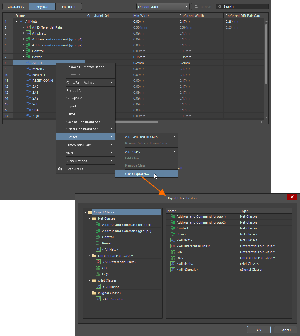
The folder-tree pane on the left side of the dialog lists supported object class types and existing object classes of each type.
- Click on the root Object Classes folder to access a summary listing in the main editing region of the dialog of all specific classes that have been defined across all object class types.
- Click on a child object class type folder to access a summary listing of all specific classes that have been defined for that type.
- Click on the entry for a specific class (or double-click on its entry in a summary list) to access controls for managing the object membership of that class.
To add a new user-defined class from the Object Class Explorer dialog, right-click within the category of class you want to create and choose Add Class from the context menu. To rename or delete a user-defined class, right-click its name and choose Rename Class or Delete Class, respectively.
Constraint Sets
To expedite the process of defining constraints for objects, the Constraint Manager provides the ability to save a set of constraints as a Constraint Set and then apply this Constraint Set to objects.
To save the set of constraints currently defined for an object as a Constraint Set, right-click a cell for this object and select the Save as Constraint Set command from the context menu. In the New Constraint Set pop-up, enter the desired name of the Constraint Set (which must be unique and not empty) and click Create.

A newly created Constraint Set will be applied to the object from which the Constraint Set has been created. To apply a Constraint Set to another object, right-click its cell and select the required Constraint Set from the Select Constraint Set sub-menu of the context menu. The cells to which a Constraint Set is applied are distinguished with a symbol in their top-left corner (e.g., ![]() ), and, in the Physical or Electrical views, the name of the applied Constraint Set will be reflected in the Constraint Set column.
), and, in the Physical or Electrical views, the name of the applied Constraint Set will be reflected in the Constraint Set column.

To edit the values of an existing Constraint Set, select an object to which this Constraint Set is applied and click the ![]() button. Change the constraint values as required and then click the Save button in the pop-up that appears to save the changes. The changes will be applied to all objects to which that Constraint Set is currently selected.
button. Change the constraint values as required and then click the Save button in the pop-up that appears to save the changes. The changes will be applied to all objects to which that Constraint Set is currently selected.

Currently defined Constraint Sets are listed in the Constraint Sets region of the Properties panel. Click the entry of a Constraint Set to show its constraint values. A Constraint Set selected in the Properties panel can be removed by clicking the ![]() button at the bottom of the Constraint Sets region. Objects to which the removed Constraint Set has been selected will keep the constraint values applied by this Constraint Set before its removal.
button at the bottom of the Constraint Sets region. Objects to which the removed Constraint Set has been selected will keep the constraint values applied by this Constraint Set before its removal.

 ).
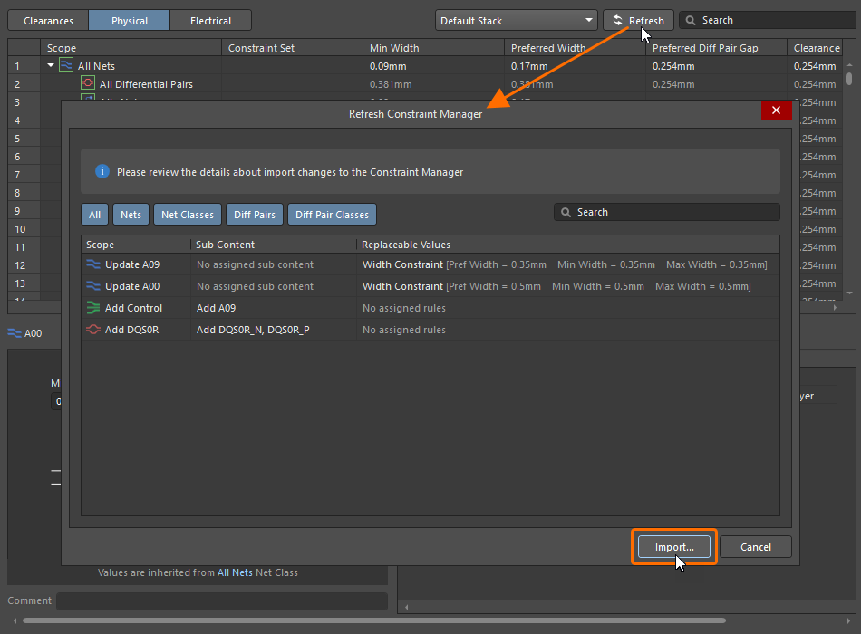
).Importing Directives from Schematics
You can import net and diff pair classes, differential pairs, and constraints from parameter set and differential pair design directives, placed and defined on your schematic source documents, into the Constraint Manager. To perform this, click the ![]() button when the Constraint Manager is accessed from the schematic side. The Refresh Constraint Manager dialog will display a summary of the import from the schematic to the Constraint Manager that will be completed by clicking the
button when the Constraint Manager is accessed from the schematic side. The Refresh Constraint Manager dialog will display a summary of the import from the schematic to the Constraint Manager that will be completed by clicking the ![]() button in the dialog.
button in the dialog.
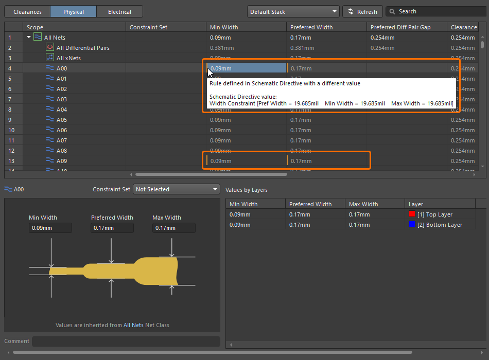
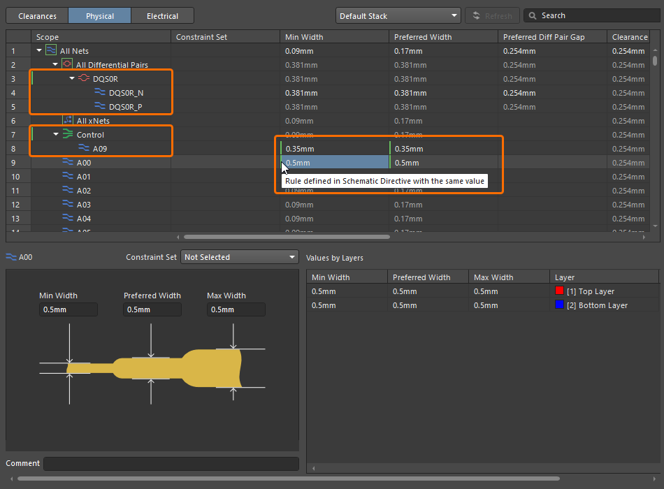
There is an indication of sync status between a constraint in the Constraint Manager and the equivalent defined in a directive placed on a schematic.
-
When an object in the schematic has a parameter set or differential pair directive placed on it, and this directive has constraint values that differ from values defined for the same object in the Constraint Manager, these values will be marked with an orange bar at the left side of the corresponding cell in the Physical or Electrical view of the Constraint Manager when the Constraint Manager is accessed from a schematic (e.g.,
 ).
).
-
When values of the constraint are in sync between the Constraint Manager and the directive, the indication changes to a green bar (e.g.,
 ).
).
There is also an indication of sync status between net classes, differential pairs, and differential pair classes imported from directives. Changes (new/removed elements) are detected, with an indication of inconsistencies requiring synchronization with an orange bar at the left of the corresponding object name (e.g., ![]() ). The in-sync status is indicated by a green bar (e.g.,
). The in-sync status is indicated by a green bar (e.g., ![]() ).
).
Notes on importing directives to the Constraint Manager:
-
Any existing constraints already defined for nets/net classes/diff pairs/diff pair classes through the Constraint Manager will take precedence and are kept when an import is processed. Therefore, if a constraint value that has been synchronized with a directive is edited in the Constraint Manager after importing, it will not be synchronized after subsequently importing again.
-
After synchronizing data by importing data from directives to the Constraint Manager and saving changes in the Constraint Manager:
-
Imported directives are distinguished in the design space by blue coloring and using a slightly different symbol (
 ).
).
-
Entries for classes and rules imported to the Constraint Manager can be filtered out using the Constraint Manager button at the top of the Properties panel's Parameters region.
-
For a parameter set directive attached to a single wire, associated data from the Constraint Manager (net/diff pair class name and rule settings) can be displayed near to that directive on the schematic sheet. For a parameter set directive including defined net classes, that is attached to a blanket, after syncing/importing with/to the Constraint Manager, it is also possible to toggle the display of net class directive information in the design space. For a differential pair directive that is attached to a blanket, it is possible to toggle the display of diff pair class and associated rules information in the design space after syncing/importing with/to directives to the Constraint Manager. Use the visibility control (
 ) at the left of the corresponding data entry in the Properties panel when the directive is selected.
-
The controls to add a new or remove an existing net class, diff pair class, or components class will be grayed out in the Properties panel for the corresponding directives.
-
The controls to add a new or edit/remove an existing rule will still be available in the Properties panel for the corresponding directives. Also, you can edit the name of a net class. To apply changes made in rules and/or net class name of an already imported directive to the data in the Constraint Manager, click the
button when the Constraint Manager is accessed from the schematic side.
-
-
For rules added to a parameter set directive that are not presented in the Physical and Electrical views, those rules will automatically be created as advanced rules presented on the All Rules view when the Constraint Manager is accessed from the PCB. The advanced rules are created upon completion of importing directives and subsequent ECO from the schematic to the PCB.
-
To allow net classes defined using directives to be imported to the Constraint Manager, the Generate Net Classes option must be enabled in the Class Generation tab of the Project Options dialog. Note that if net classes were imported to the Constraint Manager and then the Generate Net Classes option was disabled, a subsequent import to the Constraint Manager will suggest removal of the imported net classes.

Click the ![]() button. The Refresh Constraint Manager dialog will open in which you can review data to be imported to the Constraint Manager. After review, click the
button. The Refresh Constraint Manager dialog will open in which you can review data to be imported to the Constraint Manager. After review, click the ![]() button to import all data from directives.
button to import all data from directives.

Modifying Directives Imported from Read-only Documents
Directives that have been imported from read-only documents (for example, device sheets and managed sheets) cannot be modified if the Make Device Sheets In Projects Read-Only option is enabled (checked) on the Data Management - Device Sheets page of the Preferences dialog.

When the option is disabled (unchecked), the directives can be modified. After directives have been imported (with the option enabled), the rule is highlighted in blue in the Constraint Manager.

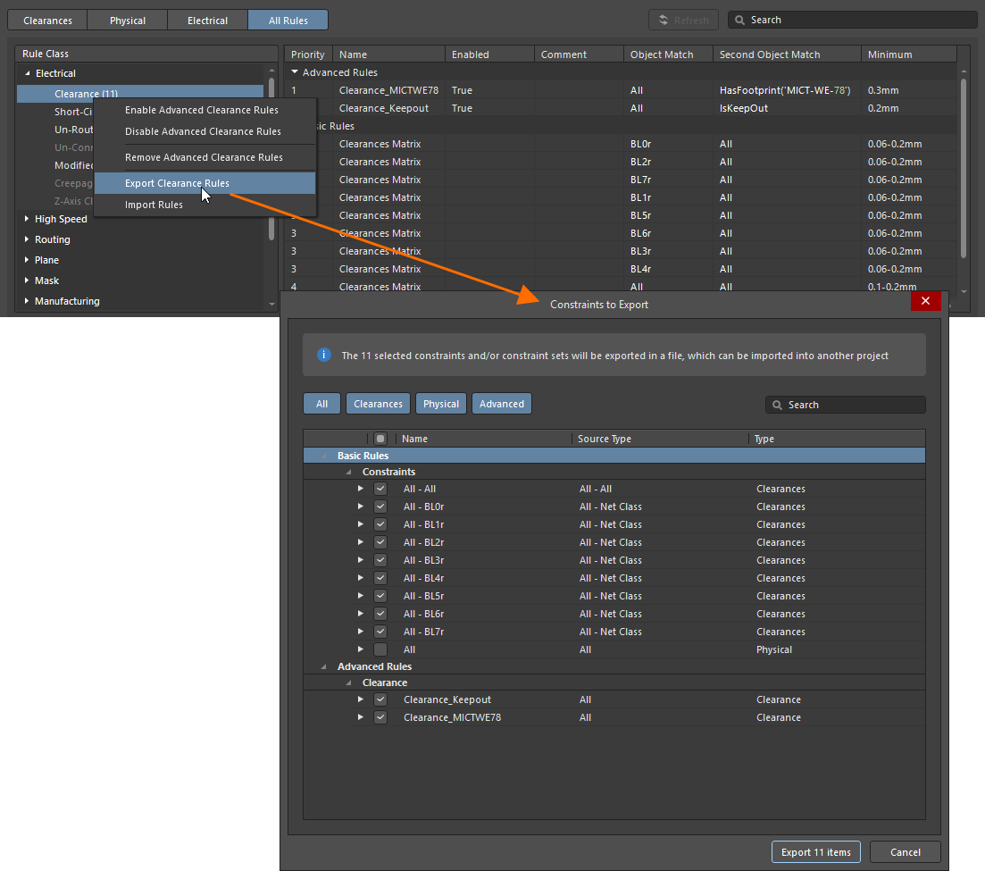
Importing and Exporting Constraints and Constraint Sets
You can import and export constraints and constraint sets between designs. To access this, right-click in the Clearances, Physical, or Electrical view of the Constraint Manager, then select Import or Export.
After selecting Import, the standard File Explorer dialog opens in which you can select the desired constraint/constraint set (*.CstrDot ) to import into your design. The Constraints to Import dialog opens in which you can select the constraints/constraint sets to import into the currect design. The selected constraints/constraint sets will be applied to corresponding objects in the target design.

 ).
).Exporting Constraints and Constraint Sets
After selecting one or more cells in the Clearances view or one or more lines in the Physical or Electrical view and then choosing Export, the Constraints to Export dialog opens with constraints and constraint sets for all objects that have been selected prior to choosing the command listed in the grid. Select the constraints/constraint sets you want to export using checkboxes (constraints related to the current view will be selected in the dialog by default). After clicking the Export items button, the standard File Explorer dialog opens in which you can name and save the constraints/constraint sets. The file will be exported with the extension *.CstrDot and can then be imported into another design.

Working with All Rules on the PCB Side
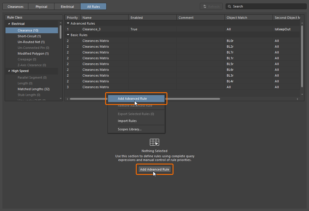
When the Constraint Manager is accessed from the PCB editor, the All Rules view is available, where a list of all rules in the PCB design is present. From here, you can create advanced rules that feature more complex query expressions in their matching scope.

 ).
).Creating a New Advanced Rule
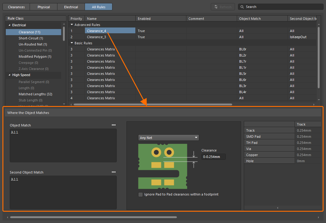
To create a new advanced rule in the All Rules view of the Constraint Manager, select Add Advanced Rule from the right-click context menu (or use the ![]() button at the lower part of the Constraint Manager when no rule is selected in the grid area), then enter a query-based matching scope and the constraint parameters in the column grid or the lower graphical representation.
button at the lower part of the Constraint Manager when no rule is selected in the grid area), then enter a query-based matching scope and the constraint parameters in the column grid or the lower graphical representation.

Managing Scopes Library
To simplify the repeated process of creating advanced rules, the Constraints Manager allows you to store query-based object-matching scopes in the Scopes Library. The library is managed using the Scopes Library dialog accessed by clicking the Edit Library button in the Scopes Library region of the Properties panel. The library is presented in the Properties panel, where custom scopes can be imported and exported as an XML file, which can then be used to populate the Scopes Library of another Altium Designer installation.

To export a scope to or import one from the library, use the commands of the menu of the ![]() button next to the Object Match / Second Object Match field in the lower part of the Constraint Manager. Once a library-based scope has been applied to a rule, the name of the scope will be shown in the Object Match / Second Object Match column in the grid area and above the Object Match / Second Object Match field. You can use the field's
button next to the Object Match / Second Object Match field in the lower part of the Constraint Manager. Once a library-based scope has been applied to a rule, the name of the scope will be shown in the Object Match / Second Object Match column in the grid area and above the Object Match / Second Object Match field. You can use the field's ![]() menu to revert the scope to its query-based format (Detach Scope).
menu to revert the scope to its query-based format (Detach Scope).

Enabling/Disabling Rules
You can enable/disable basic and advanced rules listed in the All Rules view. The Enabled column reflects the state of a rule: True (enabled) or False (disabled). Double-click a cell in the column and toggle the state of a specific rule. Cells corresponding to disabled basic rules are labeled (Disabled) and grayed out in the Physical and Electrical views.
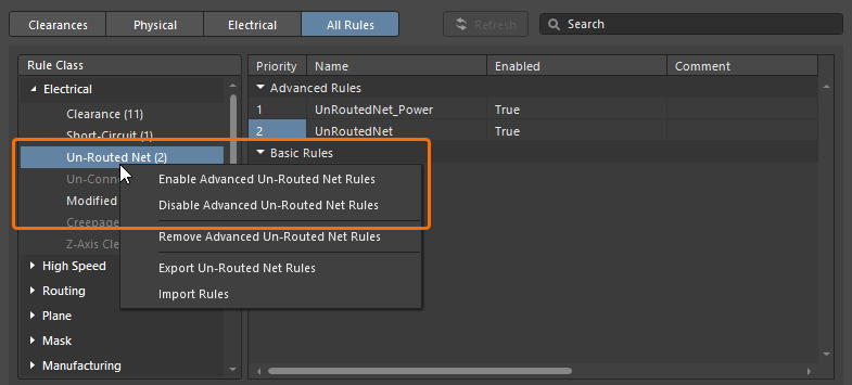
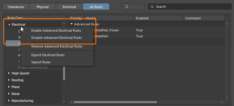
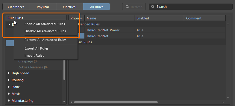
The enabled state of advanced rules of a particular type, category, or all advanced rules can also be toggled using commands available from the right-click context menu for the corresponding entry in the Rule Class tree.
|
Right-click a rule type entry in the Rule Class tree to enable/disable advanced rules of this type. Right-click a rule category entry in the Rule Class tree to enable/disable advanced rules in this category. Right-click the Rule Class heading to enable/disable all advanced rules. |
Importing and Exporting Rules
From the All Rules view, you can import and export rules (advanced and/or basic).
To export, select multiple rules in the list by using Ctrl+Click, Shift+Click, or Click, Hold&Drag, then right-click and select the Export Selected Rules (x) command (x represents the number of selected rules). You can also export all rules of a particular type, category, or all advanced rules using commands available from the right-click context menu for the corresponding entry in the Rule Class tree. After choosing an Export command, the Constraints to Export dialog opens in which you can select which rule to export into a *.CstrDot file that can be later imported into another project. After clicking the Export x Items button (x represents the number of items selected in the dialog), the standard File Explorer dialog opens in which you can define the name and location of the file. The rules will be exported into a *.CstrDot file that then be later imported into another design.
|
Right-click one or multiple selected rules to export them. Right-click a rule type entry in the Rule Class tree to export rules of this type. Right-click a rule category entry in the Rule Class tree to export rules in this category. Right-click the Rule Class heading to export all rules. |


To import, right-click in the list region or the Rule Class tree of the All Rules view and select the Import Rules command. The standard File Explorer window opens in which you select the desired *.CstrDot file; then click Open. The Constraints to Import dialog opens in which you can select the rules to import into the current design. When imported, associated custom scopes are applied automatically.

Deleting Advanced Rules
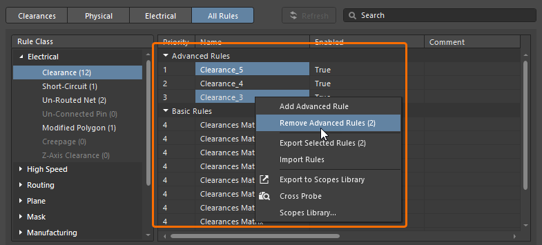
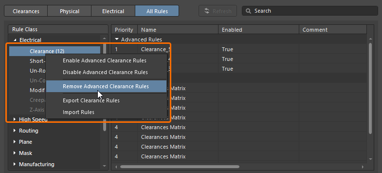
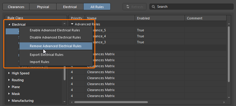
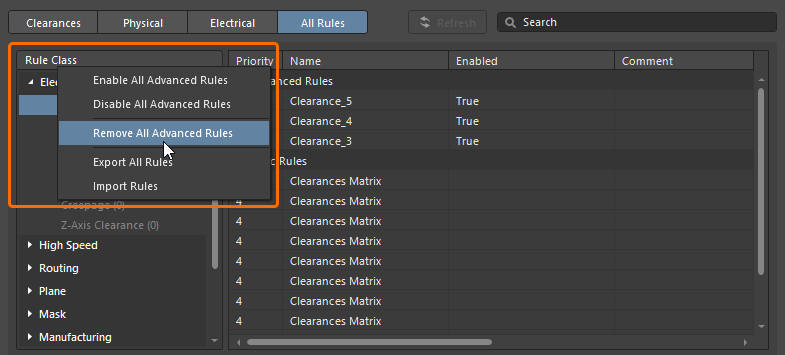
To delete the currently selected advanced rule, right-click it and select Remove Advanced Rule. To delete multiple advanced rules at a time, select multiple rules by using Ctrl+Click, Shift+Click, or Click, Hold&Drag, then right-click and select Remove Advance Rules (x). 'x' represents the number of rules that will be removed. You can also remove all advanced rules of a particular type, category, or all advanced rules using commands available from the right-click context menu for the corresponding entry in the Rule Class tree.
|
Right-click multiple selected rules to remove them. Right-click a rule type entry in the Rule Class tree to remove advanced rules of this type. Right-click a rule category entry in the Rule Class tree to remove advanced rules in this category. Right-click the Rule Class heading to remove all advanced rules. |
In each case, the rules will be deleted immediately without any confirmation.
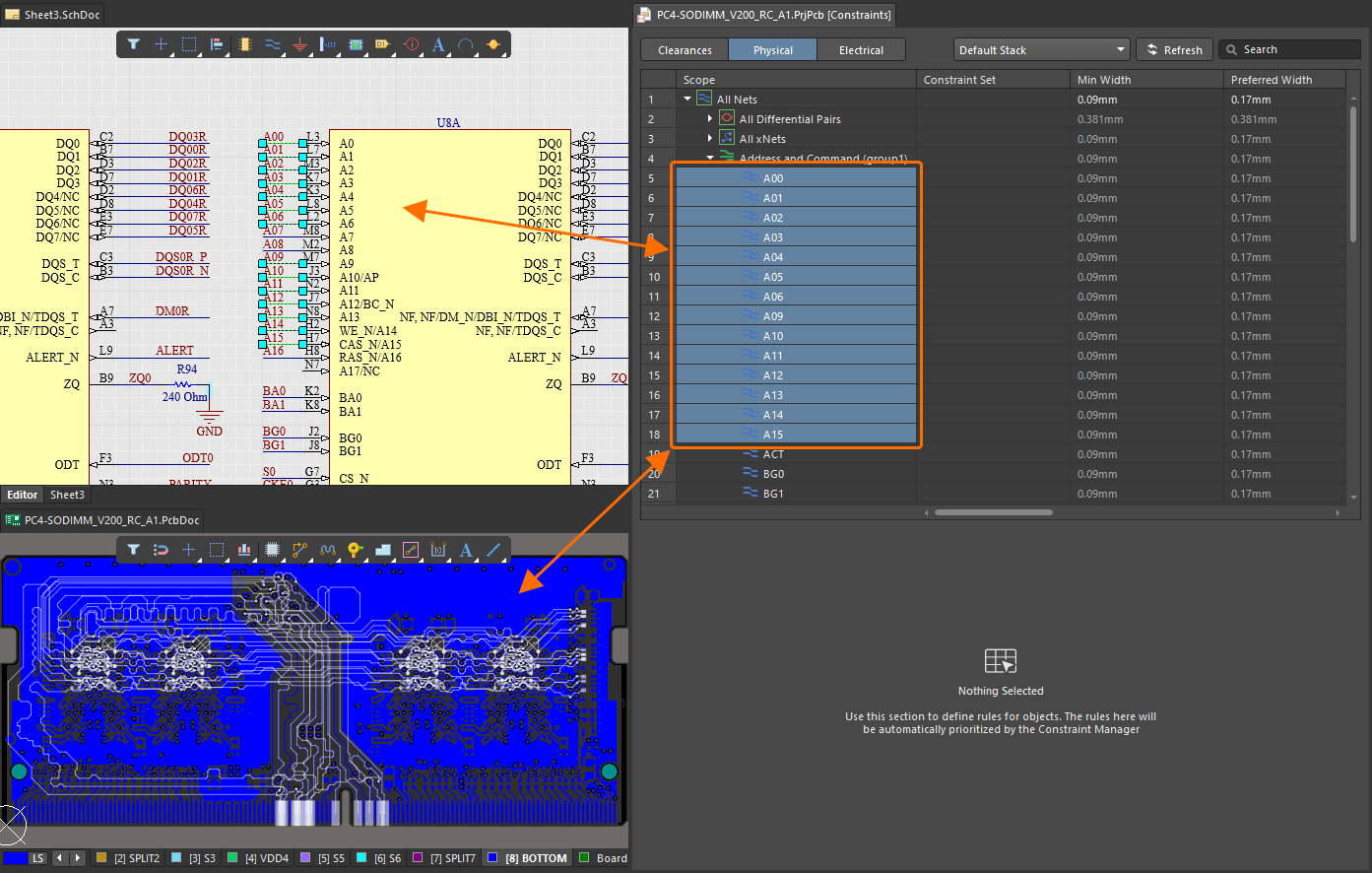
Cross-Probing
The Constraint Manager includes a cross-probe feature that will show the associated objects by visually highlighting them in the corresponding document. To cross probe to any object, right-click on its entry, then choose the Cross Probe option from the context menu or select Cross Probe from an advanced rule's ![]() menu.
menu.


Set the Cross Probe View Settings in the Properties panel to configure cross-probing settings.

Use the schematic/PCB editor Clear Filter option (right-click in the design space and select Clear Filter, shortcut: Shift+C) to reset cross-probe highlighting.
Refer to the Cross-Probing & Selecting page to learn more about cross-probing in Altium Designer.
Cross Selecting
The cross selecting feature facilitates dynamic, bi-directional object selection. When cross select mode is enabled (using the Cross Select Mode command from the Tools main menu of the Constraint Manager, the schematic or PCB editor), objects selected in the Constraint Manager are also selected in the schematic and PCB documents, and vice versa.
Refer to the Cross-Probing & Selecting page to learn more about cross selecting in Altium Designer.
Transferring Constraints between Schematic and PCB
Changes applied in the Constraint Manager are transferred between the schematic and PCB designs using the Engineering Change Order (ECO) process. Select a command to update the constraints on the other side.
-
To transfer changes from the schematic to the PCB – select the Design » Update PCB Document <PCBDocumentName> command from the main menus of the schematic editor.
-
To transfer changes (made in the Clearances, Physical, and/or Electrical views of the Constraint Manager) from the PCB to the schematic – select the Design » Update Schematics in <PCBProjectName> command from the main menus of the PCB editor.
Use the subsequential Engineering Change Order dialog to explore, validate, and execute the changes.
 ).
). ).
). ).
).Refer to the Keeping the Schematics & PCB Synchronized page to learn more.
Migrating from Design Rules to the Constraint Manager
If a PCB project uses the old rules management system (i.e., PCB Rules and Constraints Editor dialog), you can perform a one-time, one-way migration to the Constraint Manager.
Use the Design » Migrate Project to Constraint Manager Flow command from the main menus in the PCB and schematic editors. The Migration Required dialog opens to warn that the migration will take place and it cannot be undone after the ![]() button is clicked.
button is clicked.

Both PCB design rules and schematic directives will be transferred into applicable corresponding constraints within the Constraint Manager. Once the migration has successfully concluded, the Constraint Manager will be opened (in the context of which editor was active when you performed the migration).