
PCB Editor Preferences
Altium Essentials: PCB Introduction
This content is part of the official Altium Professional Training Program. For full courses, materials and certification, visit Altium Training.
The pages in the PCB Editor category of the Preferences dialog provide access to preferences relating to features and functionality with the PCB Editor.
General
The PCB Editor – General page of the Preferences dialog provides numerous controls relating to the general settings of the PCB Editor within the PCB design space.
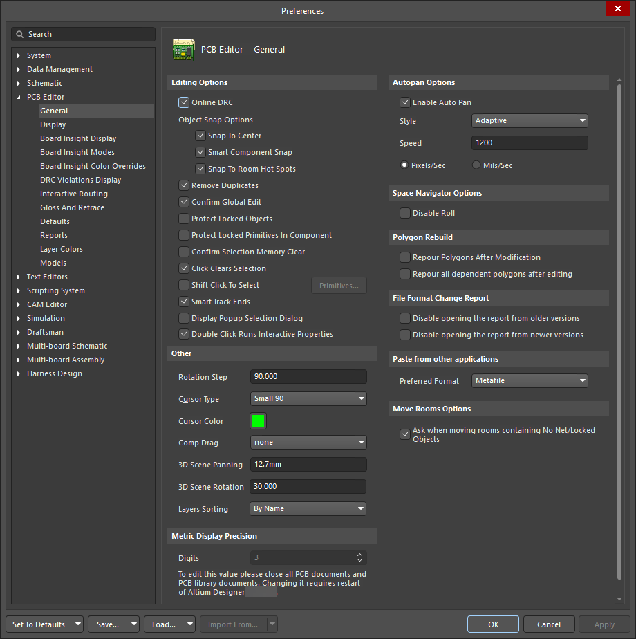
The PCB Editor – General page of the Preferences dialog
Some of this dialog's options/controls are straightforward and require no further explanation. Those that do are described below.
Editing Options |
|
| Online DRC | Enable to have software monitor all PCB design rules interactively as you work and immediately highlight any rule violations. If this option is disabled, design rule violations will not be highlighted as you work. Violations will only be highlighted when you manually run a Design Rule Check. |
| Object Snap Options |
|
| Remove Duplicates | Enable to check for and remove duplicate primitives when the system is preparing data for output. Enable this option when outputting to a vector device, such as a pen plotter or a vector photo-plotter. |
| Confirm Global Edit | Enable to open a confirmation dialog before committing a global editing action, including stating the number of objects that will be affected by the action. In the confirmation dialog, you can cancel the global edit if necessary. If this option is disabled, global editing changes will be made as soon as you click the OK button in a global editing dialog. |
| Protect Locked Objects | Enable to ignore any selected locked objects if they are part of a selection that is being moved. |
| Protect Locked Primitives In Component | Enable to prevent modification of component primitives. |
| Confirm Selection Memory Clear | Enable to open a confirmation dialog confirming that you want to clear the selection memory. |
| Click Clears Selection | Enable to clear the current selection by clicking the left button of the mouse. |
| Shift Click To Select | Enable to force using the Shift key to select specific primitives as specified by the Primitives list. Click the Primitives button to access the list. Disable this option to select a primitive normally. |
| Smart Track Ends | Enable to have smart track ends recalculate the nets so that they come from the track end rather than the shortest distance. |
| Display Popup Selection Dialog | Enable to use the Popup Selection dialog in the PCB Editor when selecting co-located objects. The Popup Selection dialog helps you easily select an object located in a 'stack' of overlapping objects (typically across different layers). |
| Double Click Runs Interactive Properties | Enable to open the Properties panel when editing placed objects using double-click; disable it to open the modal dialog when editing placed objects using double-click. |
Other |
|
| Rotation Step | This is the amount of rotation, in degrees, applied to objects floating on the cursor when the Spacebar is pressed. Edit this field to change the angle (default is 90°). The minimum angular resolution is 0.001°. Pressing the Spacebar when an object is floating on the cursor rotates the object by the set number of degrees in a counterclockwise direction. Hold the Shift key while pressing the Spacebar to rotate in a clockwise direction. |
| Cursor Type | Use the drop-down to define the shape of the "action" cursor. This cursor is displayed whenever you perform any editing action (such as placing or moving an object). Available cursors are:
|
| Cursor Color | Click to access a dialog in which you can select a color of the crosshair cursor to be used. |
| Comp Drag | Use to choose how connected tracks are handled when a component is dragged. To drag a component, select Edit » Move » Drag from the main menus and then click on the component you wish to drag. Click to view and select an option from the list.
|
| 3D Scene Panning | Displays the amount of the panning, in millimeters, applied to 3D panning controls. Default is 500mils (12.7mm). Click to edit. |
| 3D Scene Rotation | Displays the amount of rotation, in degrees, applied to 3D view controls. Default is 30°. Click to edit. |
| Layers Sorting | Use the drop-down to select if component layer pairs and mechanical layers should be sorted in the View Configuration panel. |
Metric Display Precision |
|
| Digits | This is the number of significant digits to the right of the decimal point to display when showing metric values. The last digit will be rounded as required, however, calculations within the system are always performed at the base system resolution. For example, if the initial value is calculated as "5.254667", the display will show:
|
Autopan Options |
|
| Enable Auto Pan | When enabled, when you are performing any editing action and the cross-hair cursor is active, moving the cursor past any edge of the document view window will cause the document to pan in the relevant direction. |
| Style | Use the drop-down to select the style of document autopanning.
|
| Speed | Displays the current autopanning speed. Edit this field to change the speed. The measurement is set according to the Pixels/Sec or Mils/Sec options.
|
Polygon Rebuild |
|
| Repour Polygons After Modification | Enable to automatically repour polygons that have been modified. |
| Repour all dependent polygons after editing | Enable to automatically repour any dependent polygons. |
File Format Change Report |
|
| Disable opening the report from older versions | Enable to NOT create a report when an older Altium Designer PCB file format document is opened. The report informs you that the document was created in an older version of the software and provides some information on features of the opened document that may be lost or have changed. This option is disabled by default. |
| Disable opening the report from newer versions | Enable to NOT create a report when a newer PCB file format is loaded in Altium Designer. The report informs you that the document was created in a newer version of the software and provides some information on features of the opened document that may be lost or have changed. This option is disabled by default. |
Paste from other applications |
|
| Preferred Format | Use the drop-down to choose the format when pasting from external applications.
|
Move Rooms Options |
|
| Ask when moving rooms containing No Net/Locked Objects | When enabled, a confirmation dialog will pop up when you try to move rooms without Net/Locked Objects. |
Display
The PCB Editor – Display page of the Preferences dialog provides controls relating to the functionality of the display feature within the PCB design space.

The PCB Editor – Display page of the Preferences dialog
Display Options |
|
| Antialiasing | Check to enable anti-aliasing in 3D. |
| Use Animation | Use to toggle animation on/off while zooming, flipping the board, and switching layers. |
Highlighting Options |
|
| Highlight In Full | Enable to completely highlight selected objects in the current selection color. If this option is disabled, selected objects are only outlined in the current selection color. |
| Use Transparent Mode When Masking | Enable to turn transparency on when objects are masked (i.e., you can see through them to objects on layers underneath the mask). |
| Show All Primitives In Highlighted Nets | Enable to display all primitives on hidden layers (when in single layer mode) and those primitives on the current layer for the highlighted nets. When disabled, only all primitives of the current layer (when in single layer mode) appear or all primitives on all layers (when in multi-layer mode) appear for the highlighted nets. |
| Apply Mask During Interactive Editing | Enable to mask non-selected objects during interactive editing. Masking makes it easier to focus on the objects being edited as non-selected objected objects are 'faded'. |
| Apply Highlight During Interactive Editing | Enable to highlight objects when you are in interactive editing mode (using the system Highlight color in the View Configuration panel). |
Layer Drawing Order
This region allows you to set the order in which layers are redrawn on the screen. The order that the layers appear in the list is the order in which they will be redrawn. The layer at the top of the list is the layer that will appear on top of all other layers on the screen. Select a layer in the list to alter its position using the Promote and Demote buttons as follows:
- Promote – click to move the selected layer up one position.
- Demote – click to move the selected layer down one position.
- Default – click to set the Layer Drawing Order to the system defaults.
Board Insight Display
The PCB Editor – Board Insight Display page of the Preferences dialog provides numerous controls relating to the functionality of the Board Insight feature within the PCB design space.

The PCB Editor – Board Insight Display page of the Preferences dialog
Some of this dialog's options/controls are straightforward and require no further explanation. Those that do are described below.
Pad and Via Display Options |
|
| Use Smart Display Color | Enable to have the software automatically control the font characteristics for the display of pad and via details. Disable this option to manually set the font characteristics. |
| Transparent Background | Enable to display pad/via details without any visible background. Disable this option to apply a specific color using the Background Color field. This option is not available when the Use Smart Display Color option is enabled. |
| Minimum Object Size | Displays the current minimum size (in screen pixels) of objects that will show pad and via details. This is regardless of zoom level so that at low levels of zoom, you can still maintain visibility of pad and via details. Enter the desired size or use the up and down arrows. |
Available Single Layer Modes |
|
| Hide Other Layers | When enabled, in single layer modes, only the selected layers will be shown, other layers will be hidden. |
| Gray Scale Other Layers | When enabled, in single layer modes, the selected layers will be highlighted; all primitives on other layers are displayed in gray scale. |
| Monochrome Other Layers | When enabled, in single layer modes, the selected layers will be highlighted; all primitives on other layers are displayed in the same shade of gray. |
Live Highlighting |
|
| Enabled | Enable to highlight nets when you hover the cursor over them. Disabling this option will prevent any live net highlighting.
|
Show Locked Texture on Objects
The locked texture is a visible cue that allows you to easily differentiate locked objects apart from non-locked objects. The locked object texture is shown as a 'key'. Enable the desired option
Board Insight Modes
The PCB Editor – Board Insight Modes page of the Preferences dialog provides numerous controls relating to the functionality of the Board Insight within the PCB design space.

The PCB Editor – Board Insight Modes page of the Preferences dialog
Some of this dialog's options/controls are straightforward and require no further explanation. Those that do are described below.
Display |
|
| Display Heads Up Information | Enable to turn on the Heads Up Display. The information that is displayed is typically located in the status bar such as grid coordinates, layer, dimensions, and actions. Instead of looking in the status bar, you can now see this information in the design space. |
| Use Background Color | Enable to display the Heads Up information with a transparent background. |
| Insert Key Resets Heads Up Delta Origin | Enable to reset the Delta Origin to 0, 0 at the current cursor position when the Insert key is pressed. The distance horizontally and vertically that the cursor is moved from the Delta Origin can be displayed in the Heads Up Display (Shift+D). |
| Mouse Click Resets Heads Up Delta Origin | When enabled, a mouse click resets the Delta Origin to 0, 0 at the current cursor position. The distance horizontally and vertically that the cursor is moved from the Delta Origin can be displayed in the Heads Up Display (Shift+D). |
| Hover Mode Delay | Use to set how long you want to have the cursor over an item before the hover display information appears. Click on the up or down arrow buttons (increments by 100ms) or use the slide control to increase or decrease the time delay. |
| Heads Up Opacity | Use the up/down arrow buttons (increments by 1%) or move the slide control to increase or decrease the level of opacity of the Heads Up Display mode, making it less or more visible. The preview panes at the bottom of the dialog show how the display will appear. |
| Hover Opacity | Use the up/down arrow buttons (increments by 1%) or move the slide control to increase or decrease the level of opacity of the hover display mode, making it less or more visible. The preview panes at the bottom of the dialog show how the display will appear. |
Insight Modes |
|
| Grid | The grid lists the available options for which information the Heads Up Display modes shows. Enable the checkboxes for the information types you would like displayed in the Heads Up and Hover columns. The Popup column options refer to information that will be displayed when using the object (Shift+X) and violation (Shift+V) pop-up windows. The Panel column options refer to information that will be displayed in the Properties panel. The Font column options control the display text in the Heads Up Display modes. |
Board Insight Color Overrides
The PCB Editor – Board Insight Color Overrides page of the Preferences dialog provides controls relating to the functionality of the Board Insight Color Overrides feature within the PCB design space.
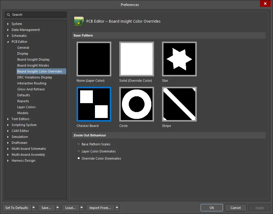
The PCB Editor – Board Insight Color Overrides page of the Preferences dialog
Base Pattern
Click to select the base pattern for the board insight color override.
Zoom Out Behavior
Use these options to determine how the nets are displayed when you zoom out:
-
Base Pattern Scales - select to scale the base pattern as you zoom out.
-
Layer Color Dominates - select to have the assigned layer color become more dominant the further you zoom out until the color is not noticeable.
-
Override Color Dominates - select to have the assigned net override color become more dominant the further you zoom out until the color is not noticeable.
DRC Violations Display
The PCB Editor - DRC Violations Display page of the Preferences dialog provides a range of controls that determine the visual functionality of the DRC Violations Display feature within the PCB design space.

The PCB Editor – DRC Violations Display page of the Preferences dialog
Violation Overlay Style
Select the visual overlay style to specify how violations appear in the PCB design space. Choose from the following options:
- None (Layer Color) - the DRC override color is ignored, leaving the default layer color visible only.
- Solid (Override Color) - the DRC override color is used, totally overriding the default layer color.
- Style A - the DRC override color is used in the display of an exclamation-type pattern, leaving the default layer color also visible.
- Style B - the DRC override color is used in the display of a cross-type pattern, leaving the default layer color also visible.
Overlay Zoom Out Behavior
Use these options to determine how the overlays are displayed when you zoom out:
- Base Pattern Scales - select to scale the base pattern as you zoom out.
- Layer Color Dominates - select to have the assigned layer color become more dominant the further you zoom out until the color is not noticeable.
- Override Color Dominates - select to have the assigned net override color become more dominant the further you zoom out until the color is not noticeable.
Choose DRC Violations Display Style
This region presents a grid allowing you to choose the display style used on a per-rule basis.
- Enabling the Violation Details field for a rule type will use the associated custom violation graphics to display the DRC violations of that rule.
- Enabling the Violation Overlay field will display the violations using the specified overlay style.
Right-click anywhere in the region to access a context menu, with commands to quickly enable or disable use of a violation display type for all rule types. You can also quickly enable the display of violations – detailed graphics or overlay styles – for only those rules currently being used in the design.
Interactive Routing
The PCB Editor – Interactive Routing page of the Preferences dialog provides numerous controls relating to the functionality of the Interactive Routing feature within the PCB design space.

The PCB Editor – Interactive Routing page of the Preferences dialog
Interactive Routing Options |
|
| Routing Conflict Resolution | These settings determine how you want the routing/sliding objects to react when they encounter an existing object. The modes enabled here will be available when you press the
|
| Interactive Routing Options | These options control how the interactive router behaves during interactive routing.
|
| General | During interactive routing, the routing engine continually glosses (neatens) the new routing. These options define the default behavior for how the routes currently being placed (or pushed) are glossed, how the corners are formed, and how strongly the router should center the pad entry/exits. Note that glossing is also applied during sliding and can also be applied to selected existing routes, the default behavior for these is configured on the Gloss and Retrace page of the Preferences dialog.
|
| Dragging | These options control how the interactive router responds: as routing objects are dragged, and as components are dragged.
|
| Interactive Routing Width Sources | These options define the default track and via size to be used during interactive routing. During routing, press the
|
| Favorites | During interactive routing, press the
|
Gloss And Retrace
The PCB Editor – Gloss And Retrace page of the Preferences dialog includes options used to configure the default behavior of glossing when it is applied during sliding, and also when it is applied to selected existing routes using the Gloss Selected and Retrace Selected commands within the PCB design space.

The PCB Editor – Gloss And Retrace page of the Preferences dialog
Gloss and Retrace Options |
|
| Gloss & Retrace Parameters | These options are applied during sliding, and also when glossing is applied by the Gloss Selected and Retrace Selected commands.
|
| Gloss Parameters | This option are applied during sliding, and also when glossing is applied by the Gloss Selected command.
|
| Retrace Parameters | These options are applied by the Retrace Selected command.
|
True Type Fonts
The PCB Editor – True Type Fonts page of the Preferences dialog provides numerous controls relating to the functionality of the True Type Fonts feature within the PCB design space.
Refer to the PCB Placement & Editing Techniques page to learn more about TrueType font support in the PCB Editor.
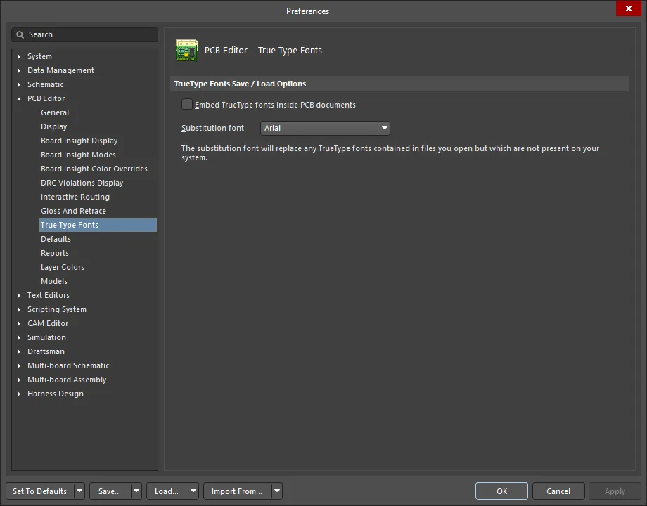
The PCB Editor – True Type Fonts page of the Preferences dialog
TrueType Fonts Save / Load Options
- Embed TrueType fonts inside PCB documents - TrueType fonts are the fonts installed on your computer. Enable this setting to save the TrueType fonts you have used in your PCB file. This will allow other machines that do not have a specific font to view the design as you have intended.
- Substitution font - the substitution font will replace any TrueType fonts contained in files you open but that are not present on your system. Use the drop-down to select the desired font.
Defaults
The PCB Editor – Defaults page of the Preferences dialog provides numerous controls relating to the default settings within the PCB design space.

The PCB Editor – Defaults page of the Preferences dialog
Default Primitives
-
Primitives - use this field to filter the presented listing of primitives.
-
Primitive List - a list of primitives that can be used in the PCB editor (filtered in accordance with the chosen entry for the Primitives field above). Click on the listed Primitives to change the available default values as described.
To view and edit the settings and options for each primitive, click on the desired entry in the Primitive List.
For more information about PCB design objects, refer to the QuickNav - PCB Design Objects page.
Additional Controls
-
Permanent - when this option is enabled, the default properties of all object types are locked and are not changed if you edit an object's properties during placement. When disabled, any changes you make to a particular object during placement (by pressing the Tab key while the object is floating on the cursor before placement to open the Properties panel/modal dialog) are used to update the default properties for that particular object type.
-
Save as - click to save the current default object properties to a custom properties file (*.dft). You will be prompted for a name and directory for the file. When the PCB Editor server is started, the current defaults are read and any changes you make to the defaults are stored in this file when you exit.
-
Load - click to load a previously saved set of default object properties. You will be prompted to navigate to and select a previously saved properties file (*.dft).
-
Reset All - click to reset the properties of all objects to the system defaults.
Reports
The PCB Editor – Reports page of the Preferences dialog provides numerous controls relating to the functionality of the Reports feature within the PCB design space.
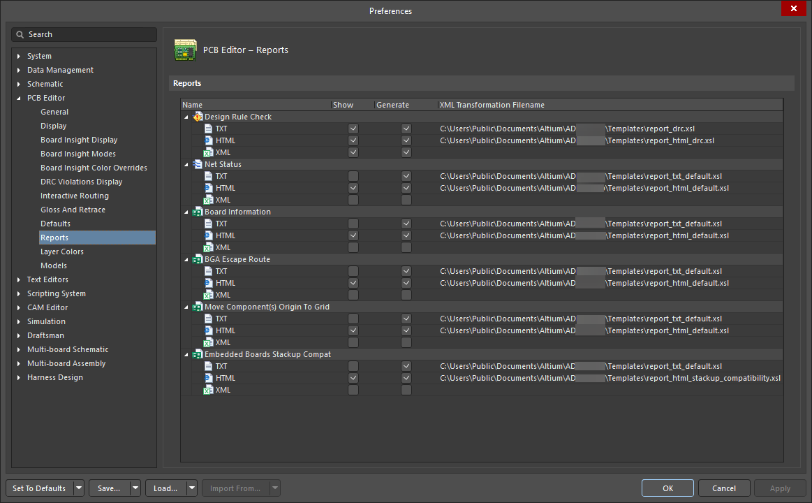
The PCB Editor – Reports page of the Preferences dialog
Reports
The PCB reports displayed in this list can be created as text, HTML, or XML files. Enable the Show option to open the report after it has been created. Enable the Generate option to generate the report. The XSL template is displayed in the XML Transformation Filename column. This path can be modified if desired.
Supported reports are:
- Design Rule Check
- Net Status
- Board Information
- BGA Escape Route
- Move Component(s) Origin to Grid
- Embedded Boards Stackup Compatibility
Layer Colors
The PCB Editor – Layer Colors page of the Preferences dialog provides controls to change the colors used for all supported board layers and system objects associated with viewing a board in 2D. Quickly change the color of a chosen layer or all layers on the fly. Alternatively, define a color profile to determine the colors assigned to each and every layer. Color profiles can be saved and loaded to enable the quick application of favorite/desired color schemes.
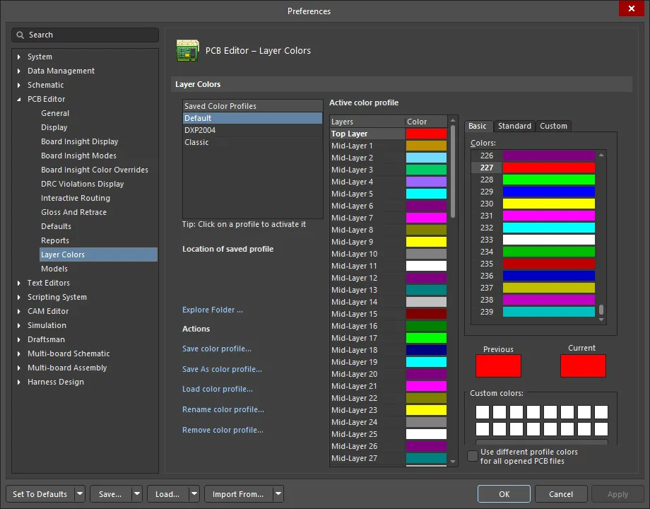
The PCB Editor – Layer Colors page of the Preferences dialog
Some of this dialog's options/controls are straightforward and require no further explanation. Those that do are described below.
Layer Colors |
|
| Saved Color Profiles | This region lists the names of the currently saved color profiles. Click on an entry to 'activate' it. This allows you to view the colors configured for the layers in that profile in the Active color profile region of the dialog and make any changes as required. |
| Location of saved profile | Displays the file path of a saved 2D color profile. Hover the cursor over an entry in the Saved Color Profiles list to see the path here. |
| Explore Folder | Click to open the folder in which the saved color profiles are located. |
| Actions | This region presents various commands for working with color profiles at the file level (
|
| Active color profile | This region provides controls to configure the layer colors for the active color profile, i.e., the profile currently selected in the Saved Color Profiles list.
|
| Selection Region | This region to the right of the layers list offers the same controls as those found in the standard Choose Color dialog. Three tabs are available, essentially giving you simple and advanced modes for choosing the required layer color. |
Models
The PCB Editor – Models page of the Preferences dialog provides numerous controls relating to Models within the PCB design space.
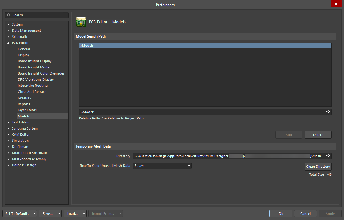
The PCB Editor – Models page of the Preferences dialog
Model Search Path |
|
| Models region | Lists all folders that will be defaulted to when linking 3D STEP model files via the Properties panel in 3D Body mode. You might consider these folders 'watched' since the software monitors changes to STEP files (*.stp, *.step) in them. |
| Models path | Click the browse icon on the right to open a dialog to browse for a folder in which to search for 3D STEP model files. Once the folder is found, add it to the Models region using the Add button. Whenever you link or embed a STEP model to a component footprint or PCB document, the folders listed in the Models region list are defaulted to. The idea of using common or central depositories for STEP model files can be beneficial, particularly in multi-user environments. |
Temporary Mesh Data |
|
| Directory | Click the browse icon to open a dialog to browse for a folder in which the software will store 3D model mesh data. Mesh data is calculated for display purposes when a 3D model is first used or created. This data is saved and is to be used whenever the model is required again. Storing mesh data in this way can improve system performance when working in the 3D design space. |
| Time To Keep Unused Mesh Data | Use the drop-down to select a maximum period of time (in days) for the system to store 3D model mesh data since its last use before deleting it. Mesh data is calculated for display purposes when a 3D model is first used or created. This data is saved and is to be used whenever the model is required again. Storing mesh data in this way can improve system performance when working in the 3D design space. |
| Clean Directory | Click to immediately empty the folder used to store temporary 3D model mesh data. |