Аннотирование проекта — это систематический и методичный процесс, обеспечивающий возможность индивидуальной идентификации каждого компонента в проекте с помощью уникального позиционного обозначения. Хотя Altium Designer способен поддерживать идентичность компонентов с использованием глобально уникальных идентификаторов (GUID), большинство разработчиков исторически используют позиционное обозначение компонента как основной способ ссылаться на него как в области схемы (логической), так и в области PCB (физической), а также в выходных данных, таких как ведомость материалов (BOM).
Существует три подхода к аннотированию проекта. Выбор инструмента аннотирования зависит от ряда факторов, включая тип проекта, личные предпочтения, а также корпоративные политики и процедуры.
Schematic Level Annotation
Аннотирование на уровне схемы (Schematic Level Annotation) использует исключительно логическое представление проекта для определения позиционных обозначений компонентов. Оно наиболее полезно для простых проектов, в которых не используются Device Sheets, но поскольку оно позволяет задавать порядок обработки, а также включает возможность дополнять существующие корпуса для многосекционных компонентов, оно также является обязательным предварительным этапом для аннотирования на уровне платы (Board Level Annotation).
Итого, используйте аннотирование на уровне схемы, чтобы:
-
Упаковывать (объединять) многосекционные компоненты.
-
Аннотировать компоненты на основе их положения в схеме.
-
Аннотировать многоканальные проекты, используя схему именования по умолчанию, заданную в параметрах проекта (Project Options).
-
Подготовить проект к дополнительному аннотированию.
PCB Annotation
Аннотирование PCB (PCB Annotation) использует физическое расположение компонентов на печатной плате для определения их позиционных обозначений. Это позволяет эффективно «закодировать» позиционную информацию в обозначении компонента и может быть очень полезно при отладке собранной платы. Иными словами, используйте PCB Annotation, чтобы аннотировать компоненты на основе их положения на плате в PCB-дизайне.
Board Level Annotation
Аннотирование на уровне платы (Board Level Annotation) обеспечивает сопоставление между позиционными обозначениями, используемыми в схеме (логический проект), и их реальными соответствиями на PCB (физический проект). Хотя Board Level Annotation можно использовать в любом проекте, оно особенно полезно для многоканальных проектов или проектов, включающих device sheets, где позиционные обозначения нельзя редактировать непосредственно на самом device sheet. Таким образом, весь проект можно переаннотировать, фактически не изменяя исходные device sheet(ы). Board Level Annotation устраняет любые конфликты аннотирования, которые могут возникать из‑за дублирующихся обозначений в проекте, и сохраняет изменения в *.Annotation текстовом файле. Оно включает дополнительные ключевые слова для настройки схем именования и позволяет применять их ко всем или только к выбранному диапазону компонентов.
Итого, используйте Board Level Annotation, чтобы:
-
Аннотировать скомпилированные компоненты в device sheets.
-
Уникально именовать все компоненты в нескольких каналах с использованием схем именования, включающих позиционное аннотирование, глобальную индексацию и другие настраиваемые параметры.
-
Назначать обозначения компонентам вручную.
Аннотирование схемы
Аннотирование схемы настраивается с помощью диалога Annotate . Диалог предоставляет элементы управления для систематического назначения позиционных обозначений всем или выбранным компонентам на выбранных листах проекта и гарантирует, что обозначения уникальны и упорядочены в соответствии с их расположением. Параметры аннотирования можно настроить для упаковки многосекционных компонентов, задания параметров индекса и суффикса, сброса позиционных обозначений на схеме, включая любые дубликаты, а также для обратного аннотирования с PCB.
Диалог Annotate открывается выполнением команды Annotate Schematics (Tools » Annotation » Annotate Schematics).

Диалог Annotate запускается из команды Annotate Schematics.
Диалог разделен на две основные области:
-
Schematic Annotation Configuration - эта область используется для настройки схемы аннотирования и области (scope) аннотирования.
-
Proposed Change List - эта область содержит список предлагаемых изменений, которые будут выполнены после принятия и запуска через Engineering Change Order (ECO).
Options and Controls of the Annotate Dialog
Конфигурация аннотирования схемы
Порядок обработки
Используйте эту область, чтобы задать требуемый метод позиционного аннотирования. При выборе метода из выпадающего списка соответствующее графическое представление динамически обновляется, показывая, как будут аннотированы компоненты. Выберите один из следующих методов позиционного аннотирования:
-
Up Then Across
-
Down Then Across
-
Across Then Up
-
Across Then Down
Когда Altium Designer обрабатывает компоненты для аннотирования, он применяет ограничивающий прямоугольник, охватывающий компонент целиком и все видимые параметры. Если порядок обработки кажется неверным, проверьте расположение параметров компонента, чтобы убедиться, что они не искажают результат.
Обрабатывать расположение по
Используйте эту область, чтобы указать опорную точку для определения расположения компонентов при вычислении порядка аннотирования. Выберите один из вариантов:
-
Designator - позиционное обозначение компонента используется как опорная точка его расположения при определении порядка обработки.
Если позиционное аннотирование работает не так, как вы ожидаете, убедитесь, что обозначения расположены корректно. Возможно, сами компоненты выровнены идеально, но смещенное обозначение приводит к нежелательным результатам аннотирования.
-
Part - центр компонента используется как опорная точка его расположения при определении порядка обработки.
Заменять подчасти
Используйте выпадающий список, чтобы выбрать, заменять ли подчасти (sub-parts) в процессе аннотирования.
Параметры сопоставления
При использовании многосекционных корпусов часто желательно упаковать как можно больше секций в минимальное число физических компонентов, поскольку это снижает общую стоимость BOM проекта. Элементы управления в этой области позволяют определить, как компоненты будут сопоставляться и группироваться, а также критерии, используемые для определения допустимых группировок.
-
Complete Existing Packages - используйте этот элемент управления, чтобы решить, будут ли и каким образом неаннотированные части включаться в существующие пакеты. В выпадающем списке выберите один из вариантов:
-
None - существующие пакеты не будут дополняться, и все новые части будут помещены в новые пакеты.
-
Per Sheet - существующие пакеты будут включать новые части только с того же листа схемы.
-
Whole Project - существующие пакеты будут включать новые части с любых листов схемы в проекте.
Чтобы упаковка многосекционных компонентов была включена в процесс аннотирования, выпадающий список Complete Existing Packages должен быть установлен в значение, отличное от None. При настройке области Completing Existing Packages следует учитывать, как у активных компонентов заданы выводы питания. Например, многие разработчики включают выводы VCC/GND в первую секцию многосекционного компонента, но затем не включают эти выводы в последующие секции. Если первая секция многосекционного компонента будет упакована в альтернативный пакет и ее sub-part будет обновлен, это может привести к неподключенным (или «висящим») цепям питания.
-
Component Parameter - этот список включает все параметры, найденные в компонентах текущего проекта. Установите флажок напротив параметра, чтобы использовать его для сопоставления частей в пакеты. Если многосекционные компоненты имеют одинаковые включенные параметры и общее значение, они будут упакованы вместе (при условии, что параметр Complete Existing Packages не установлен в None). Оставшиеся компоненты, у которых нет включенного(ых) параметра(ов), также упаковываются вместе.
Настройки по умолчанию в диалоге — дополнять существующие пакеты по Library Reference и Comment, однако вы можете выбрать любую комбинацию параметров.
-
Strictly - включите этот параметр для Component Parameter в списке, чтобы обозначить, что все компоненты must должны иметь этот параметр для сопоставления в пакет. Компоненты, у которых нет этого параметра, аннотируются как отдельные компоненты и не упаковываются.
Контекстное меню (правый клик)
-
Parameter » Enable Selected Parameters - используйте, чтобы установить флажок 'Include' для всех параметров, выбранных в списке.
-
Parameter » Enable All Parameters - используйте, чтобы установить флажок 'Include' для всех параметров в списке.
-
Parameter » Disable Selected Parameters - используйте, чтобы снять флажок 'Include' для всех параметров, выбранных в списке.
-
Parameter » Disable All Parameters - используйте, чтобы снять флажок 'Include' для всех параметров в списке.
-
Match Strictly » Enable Strict Matching On Selected Parameters - используйте, чтобы включить параметр Strictly для всех параметров, выбранных в списке.
-
Match Strictly » Enable Strict Matching On All Parameters - используйте, чтобы включить параметр Strictly для всех параметров в списке.
-
Match Strictly » Disable Strict Matching On Selected Parameters - используйте, чтобы отключить параметр Strictly для всех параметров, выбранных в списке.
-
Match Strictly » Disable Strict Matching On All Parameters - используйте, чтобы отключить параметр Strictly для всех параметров в списке.
-
Selection » Select All - используйте, чтобы выбрать все записи параметров в списке.
-
Selection » Deselect All - используйте, чтобы снять выделение со всех записей параметров в списке.
-
Selection » Invert Selection - используйте, чтобы выбрать все параметры, которые сейчас не выбраны в списке, и снять выделение с тех, которые выбраны.
Листы схемы для аннотирования
Эта область диалога содержит список всех исходных листов схемы в проекте. Элементы управления в этой области используются для определения, какие листы будут включены в процесс аннотирования и как именно будут вычисляться изменения аннотирования. Для каждого листа отображается следующее:
-
Include/Exclude checkbox - установите этот флажок, чтобы включить лист схемы в процесс аннотирования.
-
Schematic Sheet - это поле отображает имя листа схемы.
-
Annotation Scope - используйте это поле, чтобы определить область аннотирования относительно компонентов на листе. В выпадающем списке выберите один из следующих вариантов:
-
All - будут аннотированы все компоненты на листе схемы.
-
Ignore Selected Parts - будут аннотированы все компоненты, кроме тех, которые в данный момент выбраны в проекте.
-
Only Selected Parts - будут аннотированы только те компоненты, которые в данный момент выбраны в проекте.
Использование Ignore Selected Parts или Only Selected Parts требует, чтобы компоненты были выбраны в проекте до открытия диалога.
-
Order - используйте это поле, чтобы указать, какое место этот лист должен занимать в общем порядке аннотирования листов. Введите нужный номер порядка непосредственно в поле или используйте стрелки, которые появляются после щелчка в поле, чтобы прокрутить до нужного значения.
-
Designator Index Control- используйте элементы управления в этом столбце, чтобы включить использование начального индекса (установив соответствующий флажок) и задать значение индекса. Значение позиционного обозначения будет начинаться с этого значения индекса.
-
Add Suffix - используйте это поле, чтобы указать суффикс для добавления к каждому аннотированному позиционному обозначению. Поддерживаются буквенные (A, B, C...), числовые (1, 2, 3...), а также не буквенно-цифровые (_ * . %...) суффиксы, включая их комбинации.
Избегайте использования односимвольных суффиксов, таких как 'A' или '1', поскольку их легко перепутать с подчастями и/или другими значениями позиционных обозначений.
Additional Controls
-
All On - нажмите, чтобы включить все листы схемы в процесс аннотирования.
-
All Off - нажмите, чтобы исключить все листы схемы из процесса аннотирования.
-
Right-Click Menu - в контекстном меню области (по щелчку правой кнопкой) доступны следующие команды:
-
Order Alphabetically - используйте для сортировки списка схем по алфавиту. Это повлияет на соответствующую запись Order для каждого листа.
-
Order By Project Order - используйте для сортировки списка схем по порядку их следования в проекте (как показано на панели Projects ). Это повлияет на соответствующую запись Order для каждого листа.
-
All On - используйте, чтобы включить все листы схемы в процесс аннотирования.
-
All Off - используйте, чтобы исключить все листы схемы из процесса аннотирования.
Список предлагаемых изменений
-
Main List - эта область диалога перечисляет все позиционные обозначения для компонентов, содержащихся на листах, выбранных для аннотирования. Для каждой записи приводятся сведения о значениях Current и Proposed Designator , а также Sub (часть) компонента и исходный Location of Part. Значки замка (
 ) используются для обозначения заблокированных столбцов, чтобы предотвратить изменения позиционных обозначений и подчастей.
Вы можете сортировать по одному из этих «запертых» столбцов, щёлкнув по значку замка. Щёлкните один раз, чтобы сначала были перечислены все компоненты, чьи позиционные обозначения и/или подчасти доступны для изменения; щёлкните ещё раз, чтобы все элементы, которые не должны затрагиваться процессом аннотирования, оказались вверху Proposed Change List.
Установка флажка рядом с позиционным обозначением в столбце Current ('designator locked') заблокирует это конкретное позиционное обозначение от любых изменений. Аналогично, установка флажка рядом с полем Sub ('sub-part locked') предотвратит обновление этой конкретной подчасти родительского многосекционного компонента.
В контекстном меню области (по щелчку правой кнопкой) доступны следующие команды:
-
Designator » Lock Selected Designators - используйте, чтобы установить флажок 'designator locked' для всех позиционных обозначений, выбранных в списке.
-
Designator » Lock All Designators - используйте, чтобы установить флажок 'designator locked' для всех позиционных обозначений.
-
Designator » Unlock Selected Designators - используйте, чтобы снять флажок 'designator locked' для всех позиционных обозначений, выбранных в списке.
-
Designator » Unlock All Designators - используйте, чтобы снять флажок 'designator locked' для всех позиционных обозначений.
-
Part ID » Lock Selected Part ID - используйте, чтобы установить флажок 'sub-part locked' для всех позиционных обозначений, выбранных в списке.
-
Part ID » Lock All Part ID - используйте, чтобы установить флажок 'sub-part locked' для всех позиционных обозначений.
-
Part ID » Unlock Selected Part ID - используйте, чтобы снять флажок 'sub-part locked' для всех позиционных обозначений, выбранных в списке.
-
Part ID » Unlock All Part ID - используйте, чтобы снять флажок 'sub-part locked' для всех позиционных обозначений.
-
Selection » Select All - используйте, чтобы выбрать все записи позиционных обозначений в списке.
-
Selection » Select All With '?' - используйте, чтобы выбрать все записи, чьё текущее позиционное обозначение содержит ? (т.е. было сброшено).
-
Selection » Deselect All - используйте, чтобы снять выделение со всех записей позиционных обозначений в списке.
-
Selection » Invert Selection - используйте, чтобы выбрать все позиционные обозначения, которые сейчас не выбраны в списке, и снять выделение с тех, которые выбраны.
Можно выбрать несколько записей позиционных обозначений, используя стандартные приёмы множественного выбора (Ctrl+click и Shift+click).
Предлагаемые изменения вычисляются на основе настроенных параметров аннотирования и загружаются после нажатия кнопки Update Changes List (под областью).
-
Annotation Summary - эта область предоставляет сводку по аннотированию в терминах количества задействованных листов и параметров сопоставления. Она динамически обновляется по мере внесения изменений в эти области.
-
Update Changes List - нажмите, чтобы обновить основной список предлагаемых изменений новыми вычисленными изменениями на основе заданных настроек аннотирования в левой части диалога. Информационное окно покажет, сколько изменений было сделано по сравнению с предыдущим состоянием и сколько — по сравнению с исходным состоянием.
Изменения затронут только те позиционные обозначения, которые ранее не были установлены (т.е. R?, C? и т.п.), поэтому, если требуется обновить все позиционные обозначения в проекте, их следует сначала сбросить, нажав кнопку Reset All.
-
Reset All - нажмите, чтобы сбросить все позиционные обозначения в основном списке (которые не заблокированы) к их стандартным префиксам компонентов, например R?, C?, D?. Изменения будут загружены в столбец Proposed designators. Выпадающий список кнопки позволяет изменить команду на Reset Duplicates. Если два или более компонентов имеют одинаковое позиционное обозначение, все, кроме одного, будут сброшены к стандартным префиксам. Снова будет показано информационное окно с данными о том, сколько изменений было сделано по сравнению с предыдущим состоянием и сколько — по сравнению с исходным состоянием.
Обратите внимание: любые позиционные обозначения со статусом «заблокировано» не сбрасываются и не изменяются каким-либо образом.
-
Back Annotate - нажмите, чтобы открыть диалог поиска и выбора файла для обратного аннотирования.
-
Accept Changes (Create ECO) - после просмотра всех предлагаемых изменений нажмите эту кнопку, чтобы открыть диалог Engineering Change Order, в котором предлагаемые изменения перечислены как модификации в категории модификаций Annotate Component. Используйте этот диалог для проверки и выполнения ECO, завершая процесс аннотирования на уровне схемы.
Блокировка компонентов
Для неоднородных многосекционных компонентов убедитесь, что значки блокировки закрыты на панели Properties , чтобы предотвратить изменения подчастей во время аннотирования.
Параметр Strictly
Если флажок Strictly включён для Component Parameter, все компоненты должны иметь этот параметр, совпадающий при упаковке в корпус. Компоненты, у которых нет этого параметра, аннотируются как отдельные компоненты и не упаковываются.
Следующий пример иллюстрирует, как эти параметры комбинируются для получения конкретного результата:
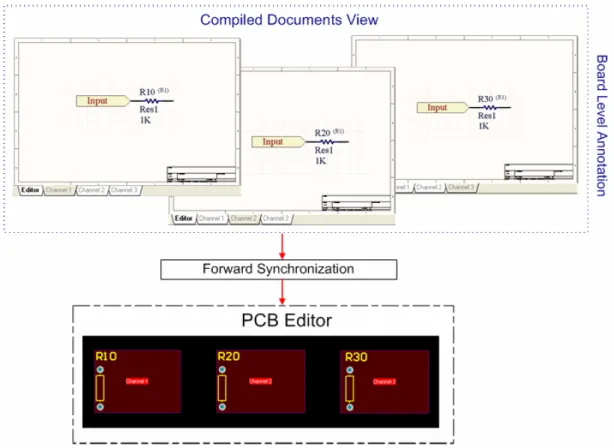
Рассмотрим проект с восемью элементами OR и восемью резисторами (как показано на изображении ниже). Элементы OR содержат параметр QuadOrGate, при этом одна группа из четырёх элементов OR имеет значение параметра Package1, а другая группа из четырёх элементов OR — значение Package2. У резисторов такого параметра нет. Включение флажка для QuadOrGate в элементе управления Component Parameter обеспечит использование этого параметра для управления тем, как компоненты упаковываются; в данном случае флажок Strictly не включён.
После запуска команды Tools » Annotation » Annotate Schematics компоненты с параметром QuadOrGate = Package1 будут упакованы в один и тот же физический компонент, а те, у которых параметр QuadOrGate = Package2, будут упакованы отдельно друг от друга. Все оставшиеся компоненты, у которых нет параметра QuadOrGate, будут упакованы вместе. В данном случае резисторы упаковываются вместе, поскольку их общий признак — отсутствие параметра QuadOrGate.

Пример упакованных компонентов, когда параметр Strictly не отмечен.
Если тот же проект аннотируется, но параметр Strictly отмечен, будут упакованы только те компоненты, у которых есть параметр QuadOrGate . В этом случае элементы OR будут упакованы, а резисторы останутся неупакованными. Следовательно, хотя параметр Strictly обеспечивает чрезвычайно тонкий контроль над процессом упаковки, в большинстве ситуаций его следует оставлять выключенным.

Пример упакованных компонентов, когда параметр Strictly отмечен.
Многосекционные компоненты могут использовать буквенный или числовой суффикс идентификатора части — т.е. U1:1, U1:2 или U1:A, U1:B. Управление стилем суффикса задаётся на странице
Schematic - General диалога
Preferences . Обратите внимание, что Preferences являются глобальными и применяются ко всем текущим открытым листам схемы.
Листы схемы для аннотирования
Предоставляется высокая степень контроля над тем, какие листы схемы и компоненты будут затронуты аннотированием, а также над тем, как именно будут вычисляться эти изменения.

Задание области аннотирования.
-
Флажок в поле слева от указанного листа схемы означает, что он будет обработан в рамках команды аннотирования.
-
Область аннотирования определяется раскрывающимся списком Annotation Scope и может быть расширена до включения всего листа схемы или ограничена (не)выбранными компонентами. Использование параметров Ignore Selected Parts или Only Selected Parts требует, чтобы компоненты были выбраны в проекте до запуска команды аннотирования.
-
Настройте порядок, в котором должны аннотироваться листы схемы, с помощью поля Order. Введите значение непосредственно в поле или используйте стрелки, которые появляются после щелчка в поле, чтобы установить нужное значение.
-
Если параметр Designator Index Control отмечен, значение позиционного обозначения будет начинаться со значения Start Index. Параметр Start Index не влияет ни на что, если параметр Designator Index Control не отмечен.
-
Дополнительный суффикс можно добавить в конец каждого позиционного обозначения, указав строку/значение в соответствующем столбце Suffix . Избегайте использования односимвольных суффиксов, таких как 'A' или '1', поскольку их легко перепутать с подчастями и/или другими значениями позиционных обозначений.
Список предлагаемых изменений
Нажмите кнопку Update Changes List, чтобы обновить Proposed Change List и иметь возможность просмотреть все изменения позиционных обозначений перед их применением. Изменения затронут только те позиционные обозначения, которые ранее не были назначены (т. е. R?, C? и т. д.). Поэтому, если требуется обновить все позиционные обозначения в проекте, их следует сначала сбросить, нажав кнопку Reset All.

Сброс позиционных обозначений перед применением настроек аннотирования.
Кнопку раскрывающегося списка Reset All также можно использовать, чтобы Reset Duplicates.
В Proposed Change List перечислены все позиционные обозначения для компонентов, содержащихся на листах, выбранных для аннотирования. Для каждой записи приводятся значения позиционного обозначения Current и Proposed, а также Sub (part) компонента и исходный Location of Part.
Установка флажка, связанного с Designator , заблокирует это конкретное позиционное обозначение от любых изменений. Аналогично, установка флажка Sub предотвратит обновление данного многосекционного компонента. Этот вариант можно использовать как альтернативу установке значка Lock на панели Properties .
После просмотра списка предлагаемых изменений нажмите кнопку Accept Changes (Create ECO), чтобы открыть диалог Engineering Change Order. После выполнения ECO изменения аннотирования будут применены к проекту.
Дополнительные команды аннотирования схем
Меню Tools » Annotation содержит ряд специализированных команд аннотирования схем. Первый пункт в группе, c, уже был рассмотрен.

Различные доступные команды аннотирования
Сброс позиционных обозначений на схеме
Если большие фрагменты содержимого были вырезаны и вставлены из разных источников в новый проект, может потребоваться сбросить все позиционные обозначения. Поскольку эта команда использует настройки из диалога Annotate , она будет применяться к объектам, ранее заданным в этом диалоге. Например, если ранее были отмечены все Schematic Sheets To Annotate, то команда Reset Schematic Designators будет применена ко всему проекту независимо от того, открыты ли сейчас листы в редакторе. Если ранее были отмечены только несколько Schematic Sheets To Annotate, то команда Reset Schematic Designators затронет только эти листы.
После запуска команды появится диалог подтверждения, в котором будет указано количество позиционных обозначений, требующих обновления, и будет задан вопрос, хотите ли вы продолжить внесение изменений. После нажатия Yes все позиционные обозначения компонентов на всех листах схем активного проекта, включенных для аннотирования, будут сброшены и примут вид: R?, C?, D?, U? и т. д.
Позиционные обозначения со статусом блокировки не сбрасываются и не изменяются каким-либо образом.
Сброс дублирующихся позиционных обозначений на схеме
При дублировании частей проекта вновь скопированные компоненты сохраняют те же значения позиционных обозначений, что и исходные. Команда Reset Duplicate Schematic Designators предоставляет быстрый способ сбросить дублирующиеся позиционные обозначения в «?». Поскольку эта команда использует настройки из диалога Annotate , она будет применяться к объектам, ранее заданным в этом диалоге. Например, если ранее были отмечены все Schematic Sheets To Annotate, то команда Reset Duplicate Schematic Designators будет применена ко всему проекту независимо от того, открыты ли сейчас листы в редакторе. Если ранее были отмечены только несколько Schematic Sheets to Annotate, то команда Reset Schematic Designators затронет только эти листы.
После запуска команды появится диалог подтверждения, в котором будет указано количество позиционных обозначений, требующих обновления, и будет задан вопрос, хотите ли вы продолжить внесение изменений. После нажатия Yes все дублирующиеся позиционные обозначения компонентов, найденные на всех листах схем активного проекта, включенных для аннотирования, будут сброшены и примут вид: R?, C?, D?, U? и т. д.
Позиционные обозначения со статусом блокировки не сбрасываются и не изменяются каким-либо образом.
Тихое аннотирование схем
Команда Annotate Schematics Quietly используется для анализа всех исходных документов схем активного проекта, включенных для аннотирования, и назначения уникального позиционного обозначения любому компоненту, у которого в данный момент отсутствует позиционное обозначение. Аннотирование выполняется «тихо» — это позволяет применить все ранее заданные настройки диалога Annotate без необходимости повторно открывать этот диалог. Это особенно полезно, если проект находится в фазе быстрого развития и разработчику нужно быстро выполнить аннотирование перед компиляцией проекта.
Принудительное аннотирование всех схем
Эта команда используется для анализа всех исходных документов схем активного проекта, включенных для аннотирования, и повторного аннотирования всех содержащихся в них компонентов в соответствии со схемой аннотирования, в данный момент заданной в диалоге Annotate.
Запуск команды Force Annotate All Schematics эквивалентен запуску команды Reset Schematic Designators с последующим немедленным запуском команды Annotate Schematics Quietly. Следовательно, команда Force Annotate All Schematics использует настройки, ранее заданные в диалоге Annotate , при определении того, какие компоненты и листы могут быть обновлены.
После запуска этой команды появится запрос подтверждения, в котором будет указано количество позиционных обозначений, которые будут обновлены в случае согласия. После нажатия Yes все позиционные обозначения компонентов на всех листах схем активного проекта, включенных для аннотирования, при необходимости будут повторно аннотированы так, чтобы соответствовать текущей позиционной схеме аннотирования, заданной в области Schematic Annotation Configuration диалога Annotate .
Обратное аннотирование схем
До появления в Altium Designer функций Design Compiler и Synchronizer изменения аннотирования исторически передавались со схемы на PCB через файл нетлиста (*.net). Изменения аннотирования, которые должны были распространяться в обратном направлении — с PCB на схему, — выполнялись посредством процесса обратного аннотирования (Back Annotation). В этом процессе используется файл Was-Is (*.WAS) или файл Engineering Change Order (*.ECO), который задает изменения, применяемые к позиционным обозначениям на схеме.
Эта команда в значительной степени избыточна, поскольку
Design Compiler и
Synchronizer являются гораздо более эффективными инструментами для управления синхронизацией проекта. Тем не менее она по-прежнему полезна для поддержки наследуемых процессов, а также для разработчиков, использующих альтернативные инструменты трассировки PCB (например, Specctra®). Узнайте больше о
создании файла Was-Is.
После запуска команды появится диалог Choose WAS-IS File for Back-Annotation from PCB. Перейдите к нужному файлу .was (или .eco) и выберите его. После нажатия Open появится информационный диалог, в котором будет указано, сколько изменений позиционных обозначений было сделано с предыдущего состояния и сколько — с исходного состояния. На этом этапе изменения фактически еще не применены. Нажмите OK , чтобы открыть диалог Annotate, где можно просмотреть предлагаемые изменения текущих позиционных обозначений, прежде чем решать, создавать ли ECO для их внедрения.
-
При повторном аннотировании позиционных обозначений на PCB каждое такое повторное аннотирование создает уникальный файл .was с датой и временем в имени файла. Это позволяет загружать несколько файлов .was последовательно — от самого старого к самому новому — и не терять синхронизацию позиционных обозначений между PCB и исходными листами схем.
-
Обратное аннотирование также можно выполнить непосредственно из диалога Annotation , нажав кнопку Back Annotate .
Нумерация листов схем
Команда Number Schematic Sheets не изменяет позиционные обозначения компонентов, а изменяет позиционные обозначения (номера) листов схем. Концептуально она связана с общей концепцией аннотирования проекта.
Нумерация листов и документов позволяет управлять обозначениями листов и сохранять их как параметры в соответствующих документах схем. Затем специальная строковая функция Altium Designer (=SheetNumber, =DocumentNumber, =SheetTotal) может использоваться для вывода этих значений на лист (например, в нижнем колонтитуле листа) в виде текстовых объектов.

Нумерация листов схем.
Процесс нумерации листов выглядит следующим образом:
Автоматическая нумерация листов (параметр проекта)
Включите, чтобы выполнять автоматическую нумерацию листов. Значения будут отображаться на панели Projects. Также можно включить автоматическую нумерацию листов, установив параметр Automatic Sheet Numbering на вкладке Options диалога Project Options.
Автонумерация листов
Нажмите кнопку раскрывающегося списка Auto Sheet Number, чтобы получить доступ к параметрам нумерации листов.

Параметры Select Numbering Scheme:
-
Display Order - листы нумеруются в том порядке, в котором они отображаются.
-
Sheets Hierarchical Structure - Depth First - листы нумеруются от верхнего уровня по каждой ветви. Сначала нумеруется верхний уровень, затем полностью нумеруется первая ветвь под верхним уровнем, затем вторая ветвь и т. д.
-
Sheets Hierarchical Structure - Breadth First - листы нумеруются в соответствии с их уровнем в иерархии. Сначала нумеруется верхний уровень, затем нумеруются все вторые уровни и т. д.
Параметры Select Numbering Method позволяют выбрать последовательные значения Increasing или Decreasing .
Автонумерация документов
Нажмите раскрывающийся список Auto Document Number , чтобы получить доступ к параметрам нумерации документов. По сути, они такие же, как параметры Auto Sheet Number, но с добавлением значений Prefix и Postfix .
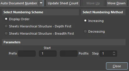
Параметры Parameters следующие:
-
Prefix - выберите префикс, который будет добавлен перед номером документа. Поддерживаются буквенные (
A, B, C и т. д.), числовые (1, 2, 3 и т. д.) и нечисловые (_, *, ., % и т. д.) префиксы, включая их комбинации.
-
Start- выберите числовое значение, с которого следует начать нумерацию.
-
Postfix - выберите постфикс, который будет добавляться к номеру документа. Поддерживаются буквенные (
A, B, C и т. д.), числовые (1, 2, 3 и т. д.) и нечисловые (_, *, . ,% и т. д.) постфиксы, включая их комбинации.
-
Step - выберите значение, на которое будет увеличиваться каждый номер документа. Например, если Start индекс задан как 1, а Step значение задано как 100, то первый номер документа будет 1, а следующий — 101 (Start + Step), затем 201 и т. д.
Обновить количество листов
Нажмите кнопку Update Sheet Count, чтобы подсчитать количество листов в текущем проекте и поместить результат в столбец SheetTotal. Количество листов будет равно общему числу листов в проекте независимо от схемы нумерации, выбранной в любом из двух предыдущих элементов управления.
Переместить вверх/вниз
Используйте кнопки Move Up или Move Down, чтобы переместить выбранный схематический документ вверх или вниз в списке. Это важно при использовании схемы нумерации Display Order для задания номеров листов или документов.
Пользовательская нумерация/именование
Если в организации используется специфическая система нумерации или именования, которую нельзя автоматизировать с помощью команд Auto Sheet Number или Auto Document Number , пользовательские имена и номера листов можно напрямую ввести в поля SheetNumber или DocumentNumber .
Нумерация листов схемы и Device Sheets
Номера листов или документов нельзя настроить для Device Sheets, когда они доступны только для чтения (состояние по умолчанию); в диалоге Sheet Numbering For Project они будут заштрихованы, что указывает на невозможность обновления. Когда Device Sheets переведены в редактируемый режим, штриховка убирается, и нумерацию листов и документов можно настраивать как обычно.
Управление отображением позиционного обозначения на PCB
Расширенные строки Designator в многоканальном проекте может быть утомительно размещать в PCB Editor. Можно либо выбрать параметры именования, дающие короткое имя, либо вместо этого отображать исходное логическое обозначение компонента. Например, C30_CIN1 будет отображаться как C30. В этом случае потребуется добавить на плату другое обозначение, чтобы указать отдельные каналы — например, обвести каждый канал рамкой на слое component overlay.
Вы можете выбрать отображение логических или физических позиционных обозначений на PCB с помощью раскрывающегося списка Designator Display в области Other панели Properties в режиме Board . Если выбрать отображение логических обозначений для компонентов в многоканальном проекте, они будут показаны на PCB и во всех формируемых выходных данных, таких как печать и Gerber. Однако уникальные физические обозначения всегда используются при формировании ведомости материалов (Bill of Materials).

Синхронизация проекта — завершение процесса аннотирования
Прямая синхронизация проекта (Direct Design Synchronization) — предпочтительный способ поддерживать совпадение позиционных обозначений между схемой и PCB, если только у вас нет доступа одновременно к редакторам схемы и PCB. Direct Design Synchronization напрямую сравнивает компоненты и связность схемы с PCB, формируя список различий. Затем генерируется список изменений, необходимых для устранения этих различий, в виде ECO (Engineering Change Order). Файл ECO описывает различия между текущим и требуемым состоянием проекта и может быть выполнен, обновляя целевой документ и приводя проект к синхронизации.
Прямая и обратная синхронизация
Термины Forward Synchronization и Back Synchronization описывают направление, в котором при синхронизации данных передаются аннотации и изменения проекта. Если представить поток проектирования, который начинается со схемы и ею же определяется, то Forward Synchronization — это процесс переноса изменений, сделанных в Schematic Editor, вперед на PCB. Back Synchronization — это процесс переноса изменений, сделанных на PCB, назад в Schematic Editor.
Forward Synchronization
Несколько причин, по которым может потребоваться синхронизировать данные со схемы на PCB:
-
В Schematic Editor добавлен новый компонент, и он требуется в разводке PCB.
-
Вы впервые аннотировали схему или сделали это после последней синхронизации проекта.
-
В многоканальном проекте вы изменили Project Options, чтобы изменить физический (PCB) стиль именования.
-
Вы впервые выполнили Board Level Annotation или сделали это после последней синхронизации проекта.
Синхронизация схемы вперед с проектом PCB
Выберите один из следующих способов синхронизировать схему вперед с проектом PCB:
-
Выберите Update PCB Document в меню Design в Schematic Editor. Если между ними и целевым PCB Document есть различия, откроется диалог Engineering Change Order со списком модификаций, необходимых для синхронизации PCB со схемой. Нажмите Execute Changes, чтобы синхронизировать проект.
-
Выберите Import Changes в меню Design в PCB Editor — будут импортированы изменения из Schematic Documents в документ PCB.
Back Synchronization
Back Synchronization выполняется, когда вы аннотировали или изменили проект PCB и хотите обновить схему.

Синхронизация проекта PCB назад со схемой
Выберите один из следующих способов синхронизировать проект PCB назад со схемой:
-
в PCB Editor выберите Update Schematics в меню Design . По умолчанию в диалоге Project Options на вкладке ECO Generation tab установлен флажок Push Component Designator Changes to Annotation File (if any), поэтому изменения, сделанные в PCB Editor, будут отправляться только в файл аннотаций и, в конечном итоге, в Compiled Documents при компиляции. Снимите этот флажок, чтобы отправлять изменения только в исходный документ схемы (Editor view).
-
В Schematic Editor выберите Tools » Annotation » Annotate Schematics, затем нажмите кнопку Back Annotate в диалоге Annotate dialog. Выберите файл WAS-IS, созданный при повторном аннотировании позиционных обозначений в среде PCB.
Это устаревший инструмент. Предпочтительный метод синхронизации проекта — команда Design » Update Schematics.
-
В Schematic Editor выберите Tools » Annotation » Board Level Annotate, затем нажмите кнопку Back Annotate в диалоге Board Level Annotate. Выберите файл WAS-IS, созданный при повторном аннотировании позиционных обозначений в среде PCB.
Это устаревший инструмент. Предпочтительный метод синхронизации проекта — команда Design » Update Schematics.
-
В Schematic Editor выберите Tools » Annotation » Back Annotate Schematics. Выберите файл WAS-IS, созданный при повторном аннотировании позиционных обозначений в среде PCB.
Это устаревший инструмент. Предпочтительный метод синхронизации проекта — команда Design » Update Schematics.
Back Annotate Schematics синхронизирует изменения аннотаций, выполненные в PCB Editor, со схемой. Эта функция полезна, когда невозможно держать редакторы PCB и схемы открытыми одновременно — например, когда PCB и схема разрабатываются людьми, находящимися в разных местах.
Традиционные методы синхронизации проекта
Altium Designer поддерживает традиционный подход к синхронизации проекта через промежуточные файлы (netlist и WAS/IS). Forward Synchronization данных аннотаций можно выполнить с помощью файла netlist, а Back Synchronization — с помощью файла WAS/IS (в котором перечислено, каким было каждое позиционное обозначение WAS и каким оно стало IS). Предпочтительный метод синхронизации проекта — Direct Design Synchronization.
Связывание компонентов с помощью уникальных идентификаторов
Если вы повторно аннотировали проект, позиционные обозначения компонентов на схеме или в скомпилированных документах больше не будут совпадать с позиционными обозначениями компонентов на PCB, поэтому для успешного завершения проекта требуется синхронизация. Вместо того чтобы полагаться на само позиционное обозначение как на ключевое поле, связывающее символ на схеме с соответствующим посадочным местом на PCB, Altium Designer может поддерживать синхронизацию проекта через систему Unique IDentifier (UID). UID — это генерируемое системой значение, которое уникально идентифицирует исходный компонент и сопоставляет каждый компонент схемы с соответствующим компонентом PCB.
Когда компонент размещается на листе схемы, ему автоматически назначается UID. При первой передаче информации о компонентах из исходных документов схемы в пустой документ PCB информация UID каждого компонента схемы назначается соответствующему компоненту PCB.
Refactoring позволяет преобразовывать Device Sheets в Schematic Sheets и наоборот, сохраняя Unique ID листа и его компонентов. Кроме того, можно выполнять рефакторинг (или перенос) подцепей на другие листы схемы в текущем проекте, сохраняя Unique ID подцепи. Команда Refactor находится в меню Edit .
Функция синхронизации в Altium Designer, запускаемая командой Design » Update, использует эти UID для сопоставления каждого компонента схемы с его эквивалентом на PCB. Затем обновления/изменения проекта можно внедрять с помощью Engineering Change Orders (ECO). ECO содержит перечень всех модификаций, необходимых для внесения изменений в один или несколько документов проекта в соответствии с запрошенным действием синхронизации. ECO используются для обновления проекта в различных ситуациях, например:
-
Обновления проекта SCH → PCB.
-
Выполнение обновлений аннотаций для позиционных обозначений компонентов на схеме и в скомпилированных документах.
-
Внедрение обновлений параметров с помощью Parameter Manager (Tools » Parameter Manager).
-
Обновление параметров данными, хранящимися в исходных библиотеках или в базе данных компании. Каждый раз, когда вы сравниваете схему и PCB (например, при выборе Design » Update), Altium Designer сначала сопоставляет компоненты с одинаковым UID. Если обнаруживаются компоненты без общего UID, вы получите уведомление, и приложение предложит попытаться сопоставить их по позиционному обозначению. Пока вы не назначите совпадающий UID и для схемы, и для PCB, это сообщение будет появляться. Управление Unique ID и их соответствием выполняется в диалоге Edit Component Links (Project » Component Links).

Обратите внимание, что это диалоговое окно можно открыть только при активном документе PCB, поскольку изменения UID всегда применяются к плате, а не к схеме. Используйте это окно на любом этапе проектирования, чтобы просмотреть связи между компонентами и убедиться, что компоненты в разных документах сопоставлены корректно, а также чтобы назначить совпадающие UID компонентам, которые в данный момент не сопоставлены.
Если вы планируете повторно выполнить аннотирование либо схемы, либо PCB, крайне важно сначала убедиться, что UID совпадают, поскольку после изменения всех позиционных обозначений на схеме или PCB UID становится единственной информацией, которую можно использовать для связывания компонента на схеме с его эквивалентом на PCB.


 Локализовано с помощью ИИ