
Professional PCB Design
Design with everything you need to preserve your intent, maintain your flow, and stay predictable as complexity increases.
Are You A Student? Enroll in the Student Lab

Start Designing Fast

Complex Design Made Simple
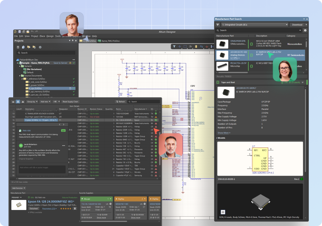
- Design rules, stack-up, sourcing data, and verification details are visible together.
- Complex boards become easier to understand so you can see how the design is built.

Your Complete PCB Design Toolkit
- Schematic capture, PCB layout, ActiveBOM, and manufacturer parts come together in a complete PCB design kit trusted by engineers.
- You have everything you need to deliver boards from concept to production with the gold standard for PCB Design.
Core Key Capabilities
Confident Change Without Breaking Design
Seamless workflows between schematic capture and PCB design make on-the-fly changes fast and simple.
Professional Outputs Without Friction
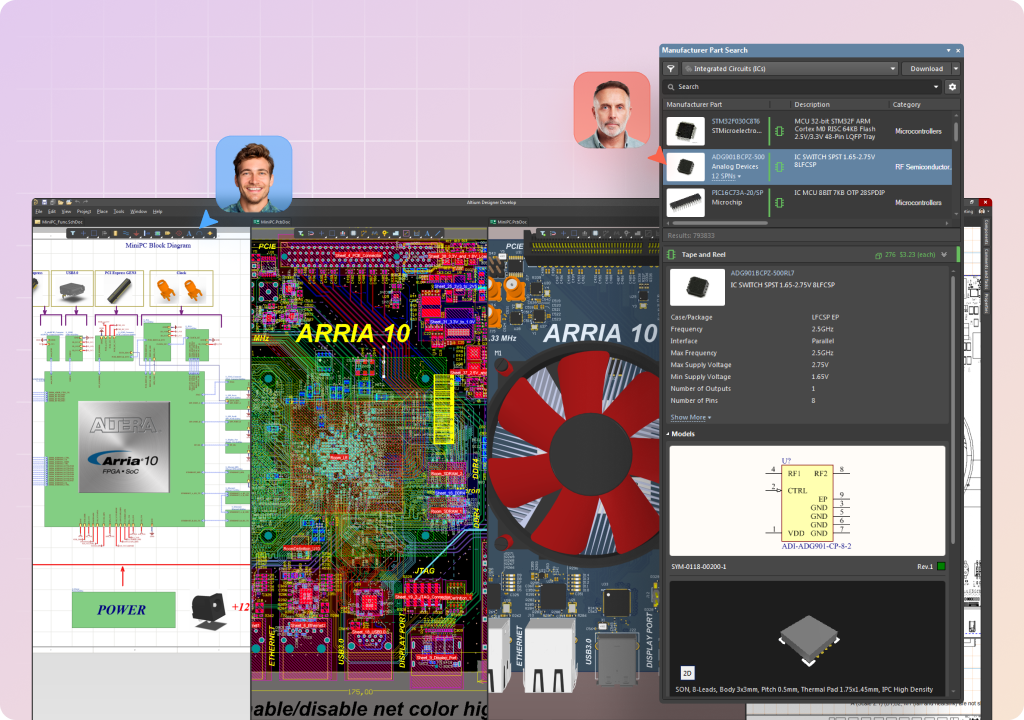
Professional Outputs Without Friction
Generate manufacturing files, drawings, 3D visualization, and release artifacts directly from your design environment. Clean, repeatable, and ready for confident release.
System-Level Design Without Integration Surprises
System-Level Design Without Integration Surprises
Design and validate connectivity across multiple boards with integrated harness workflows and system-level checks that reduce late-stage integration surprises.
Flexible Support Without Mandates
Flexible Support Without Mandates
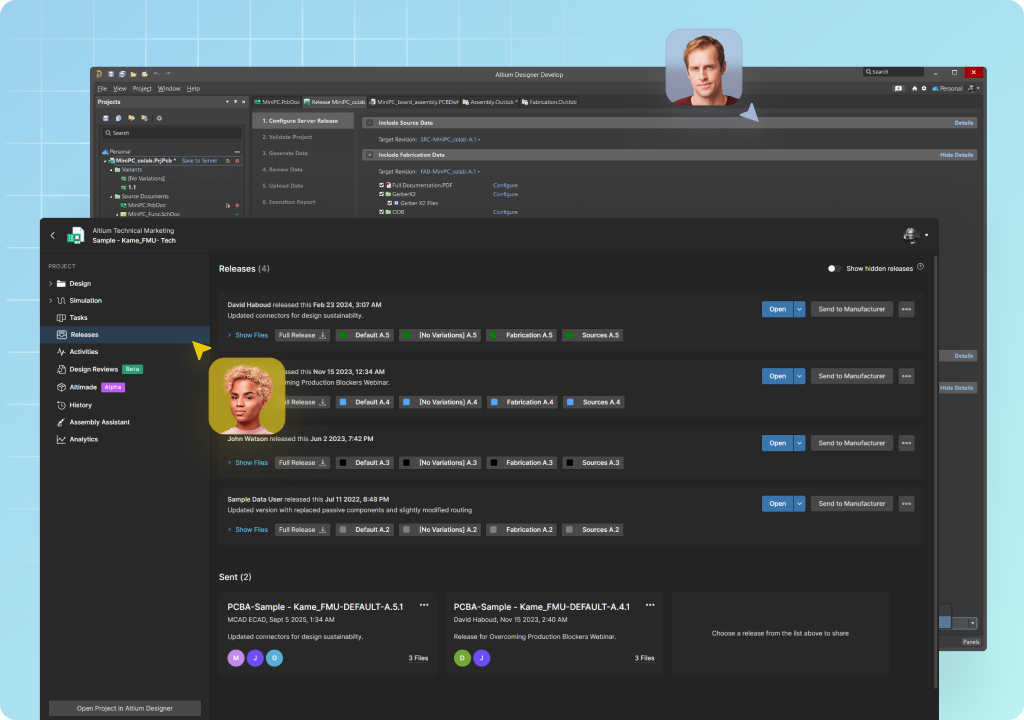
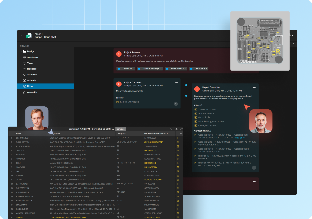
Access built-in version clarity, contextual design reviews, and secure sharing when needed—reducing version confusion and stress without disrupting how you work day to day.
Get Started with Altium Develop
Create a workspace for $995 per year. Invite unlimited collaborators for free.
Start your 30-day evaluation today.