
Keysight 的 Power Analyzer
PCB 设计布局的实际性能取决于多种因素,其中许多都可以通过一系列 PCB 设计分析工具(例如后布局 Signal Integrity analysis)在相当程度上进行预测。然而,经常被忽视的,或只是被简单归结为“经验法则”的,是如何为电路板的直流电源传输系统制定最有效的布局设计。这涉及对板上铜皮区域的设计判断:这些铜皮既为电路提供直流电源轨,也为其提供接地/公共回流路径以返回到直流电源。期望的结果是实现一种高效设计,从而保持设计中直流电源布局的完整性。
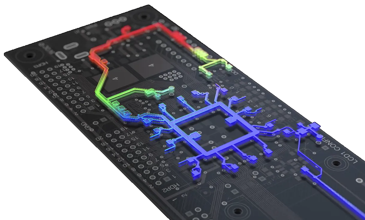
随着现代数字设计包含高速电路、多个器件、器件密集的电路板以及多路电源轨,设计的直流电源分配网络所承受的要求,使得其设计需要采用更具分析性的方式。对电源传输网络(PDN)的直流分析,或其直流电源完整性(PI-DC)的结果,基本目标是确保从电压源到负载的路径上提供了足够的铜——换句话说,确保板上的平面、走线和过孔具有足够的尺寸(及特性),以满足板上器件的功耗需求。
幸运的是,可以通过使用直流电源完整性(PI-DC)仿真工具来消除对 PCB 供电网络评估中的猜测。该工具会基于板级设计的电气与物理属性分析其直流性能,并帮助工程师回答关键设计问题,包括:
-
识别并解决直流电压与电流密度问题。
-
计算多网络及回流路径的相互作用。
-
在 PCB 编辑器中可视化电压与电流密度分布,并识别热点。
-
在板上任意位置检查电压、电流密度以及过孔电流。
-
生成分析仿真结果报告。
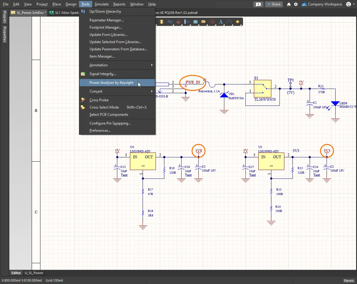
要在 Altium Designer PCB 设计环境中直接执行直流电源完整性分析,首选方案是 Power Analyzer by Keysight。
该工具由 Keysight Technologies 提供支持,可直接与 Altium Designer 集成,从而对当前 PCB 项目进行 PI-DC 仿真与分析。Power Analyzer 不再依赖简单的截面积计算来确定电源网络的载流能力,而是先对铜结构进行精确建模,然后计算整个 PCB 上的电源传输电压与电流。结果以可视化与表格两种形式呈现,工程师可利用这些反馈快速调整走线宽度、铜厚以及过孔属性,以确保达到其设计所需的直流供电完整性。
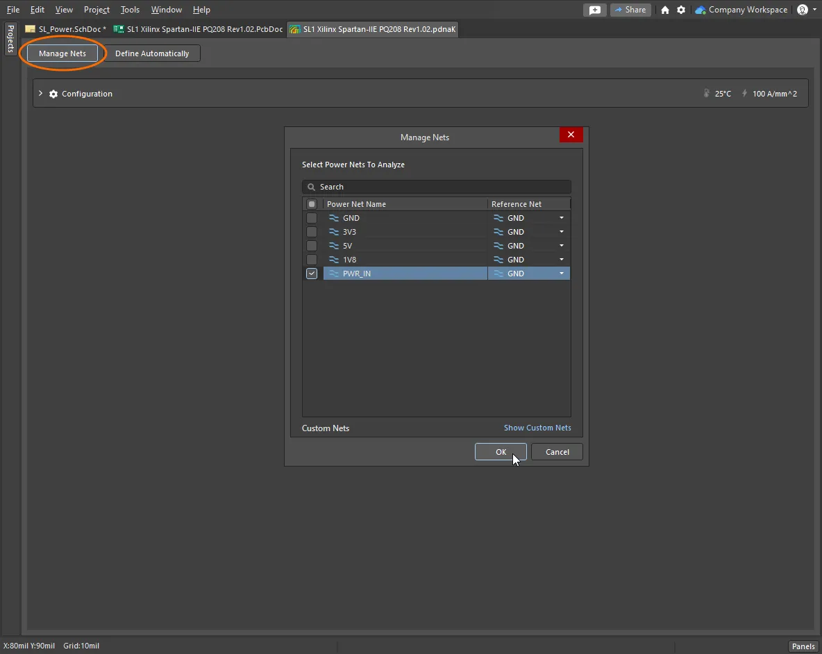
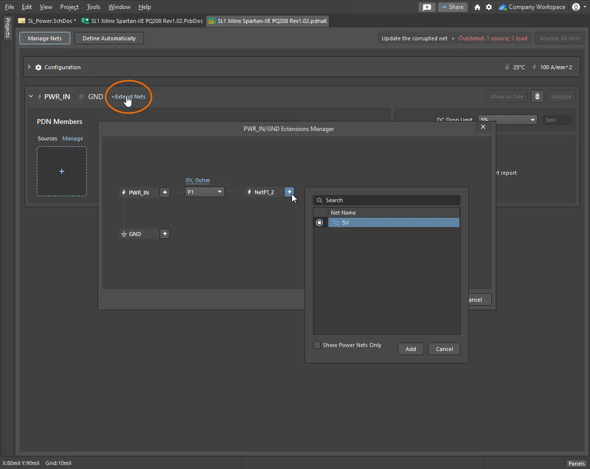
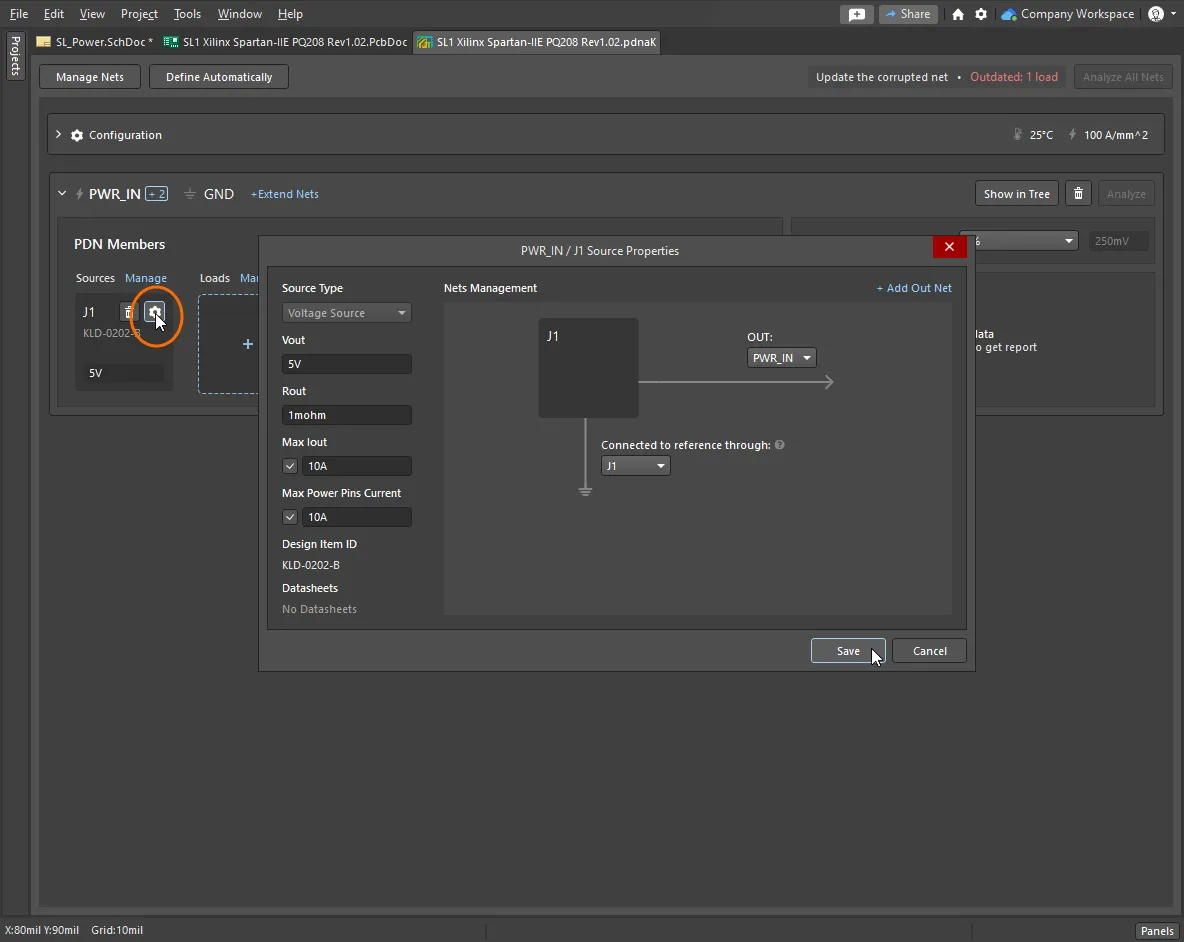
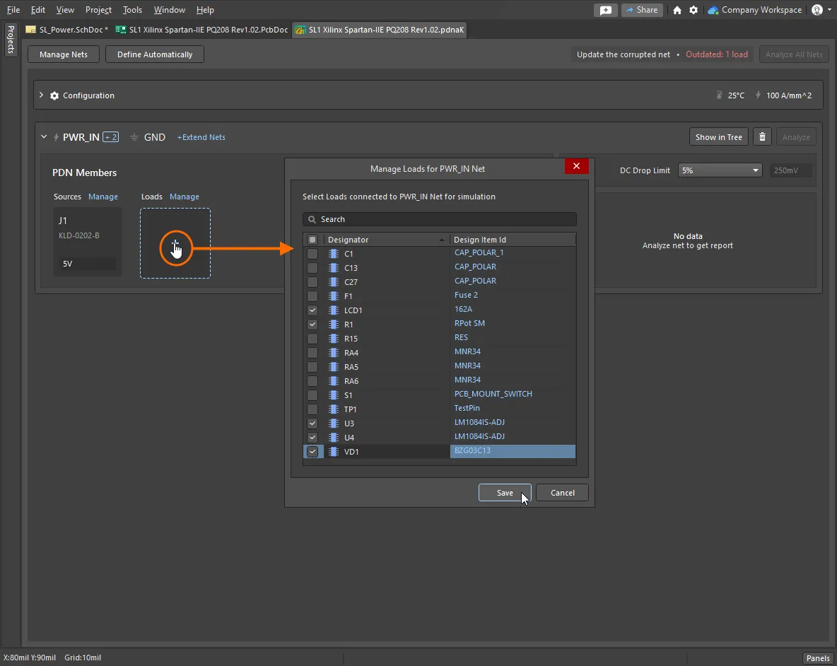
要在 Altium 中执行电源完整性分析,工程师首先需要为整个供电系统创建分层网络,识别每一条电源与回流网络、各个源与负载,以及电源网络各段中存在的任何串联元件。一旦网络与配置设置完成,Power Analyzer 就可以检查整个网络。
配置电源网络
Power Analyzer 会检查电源网络中沿铜路径的能量流动。电源网络通过识别并配置各类网络元素来定义,包括网络(net)、电源(source)、任何串联器件以及负载(loads)。要配置电源网络:
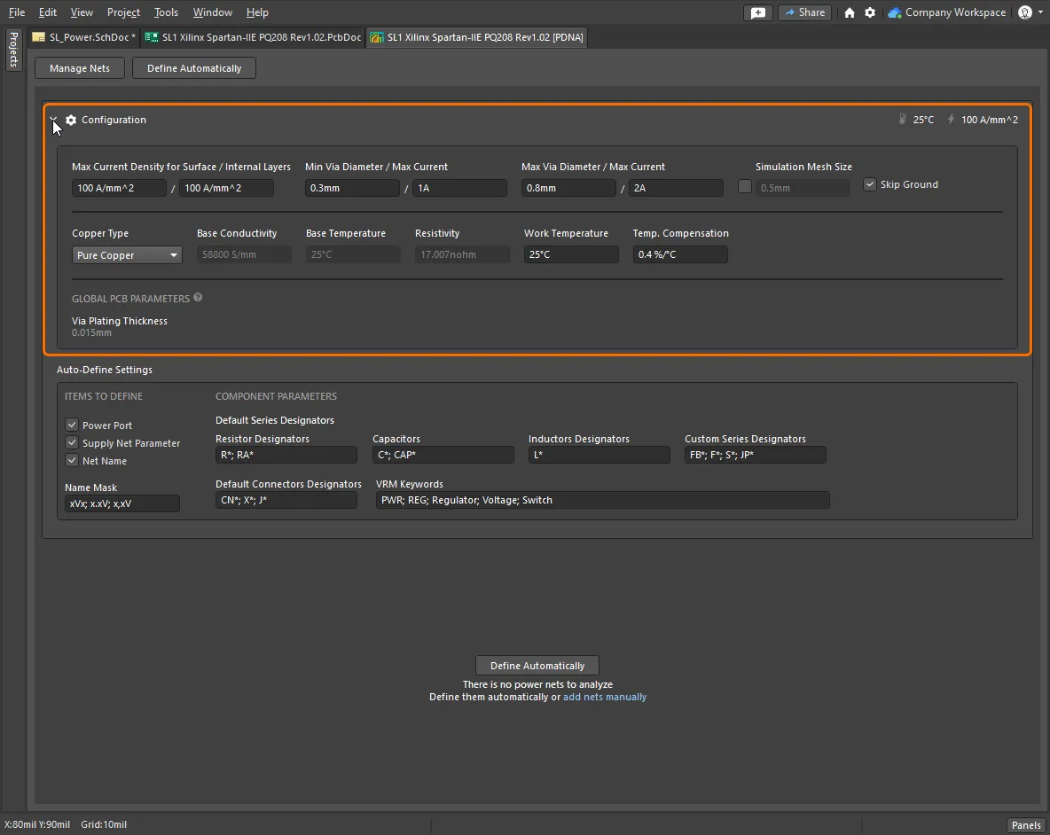
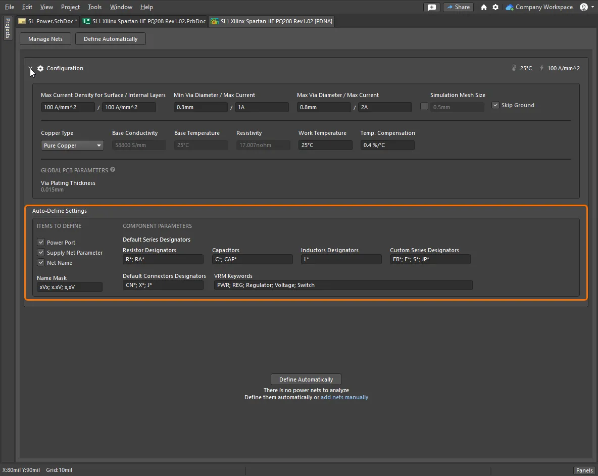
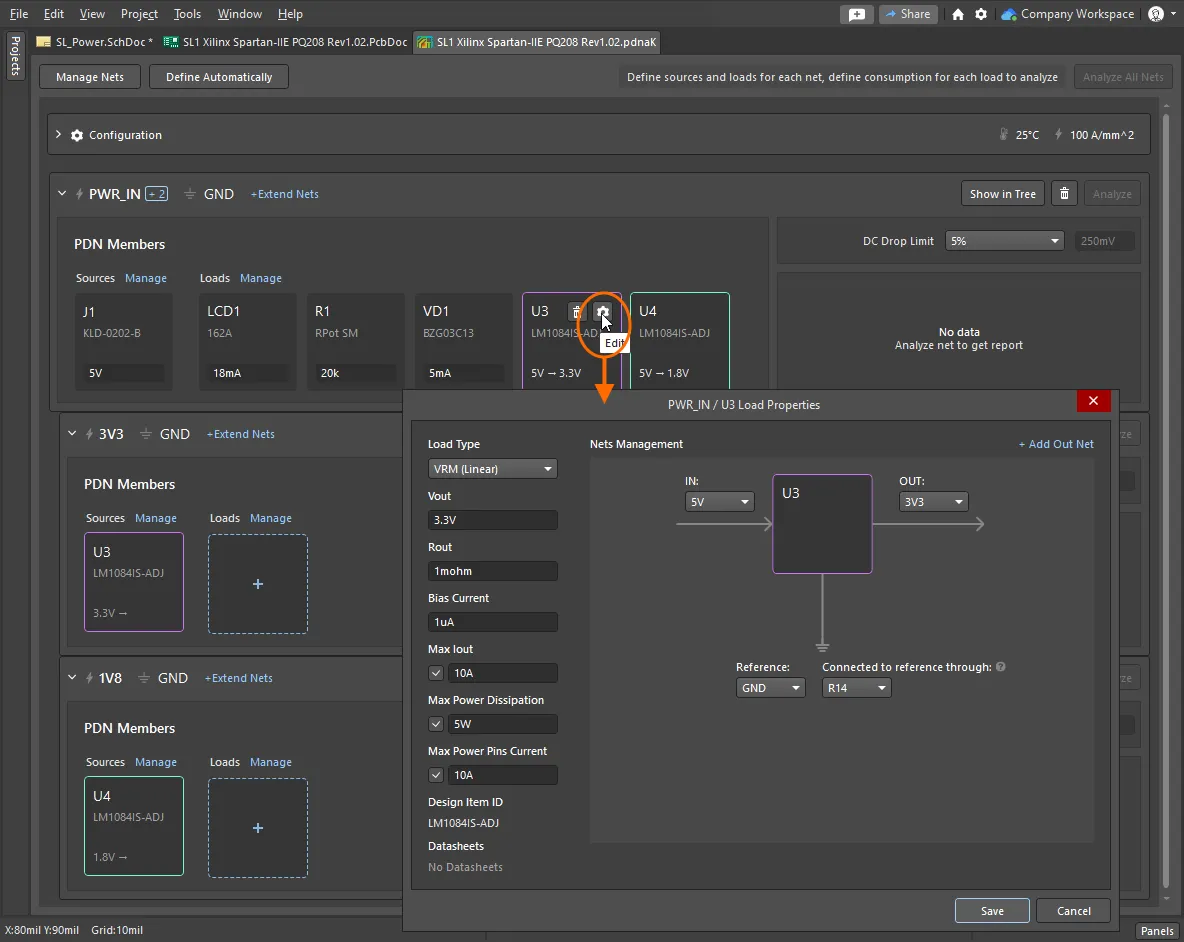
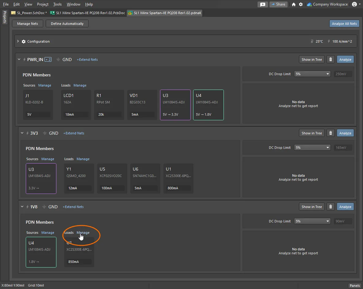
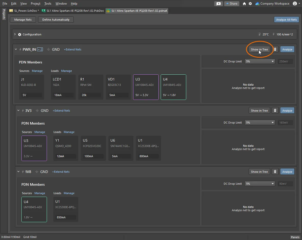
向项目添加一个 Analysis 文档分析是在 Power Analyzer by Keysight 文档( 配置板属性Power Analyzer 需要了解电路板的物理属性,例如允许的电流密度、铜的类型、工作温度等。请确认在 analyzer 文档的 Configuration 部分中定义的默认值适用于你的设计。 自动识别电源网络Power Analyzer 可以尝试自动识别电源网络。为此,它需要知道如何识别电压调节器、连接器以及串联元件等电路元素。除了使用诸如器件位号前缀等线索外,你还可以为某些器件添加参数,以增强自动检测过程。了解更多:Configuring the Auto-Define Settings。 选择电源网络(Power Net)点击 扩展网络(Net)如果电源网络经过保险丝等串联元件,请扩展该网络并识别串联元件与链式网络。了解更多:extending a net。 识别并配置电源(Source)每条电源网络都从一个电源开始,例如连接器。在 Add Source 对话框中启用该电源,然后点击齿轮图标配置该电源。了解更多:identifying and configuring the Source。 识别负载(Loads)从主要耗流器件开始,包括电压调节模块(VRMs)。了解更多:identifying the Loads。 配置负载与 VRMs点击齿轮图标打开 Load Properties 对话框,并配置每个负载。当某个器件被配置为 Voltage Regulator Module (VRM) 时,会在层级结构中自动创建一个子电源网络,并以该 VRM 作为电源。 识别子电源网络中的负载确保每条电源网络中都包含主要负载器件。 确认电源网络点击 准备分析检查树状结构(Tree),以直观确认每个电源网络都已完整。要从一个电源网络切换到另一个电源网络,请点击 Power Analyzer by Keysight 链接返回电源网络文档,并为每条电源网络选择对应的 Tree。完成后,即可开始分析电源网络。 |
分析电源网络
一旦定义好电源网络,就可以分析电路板上及板内的直流电源分配情况。
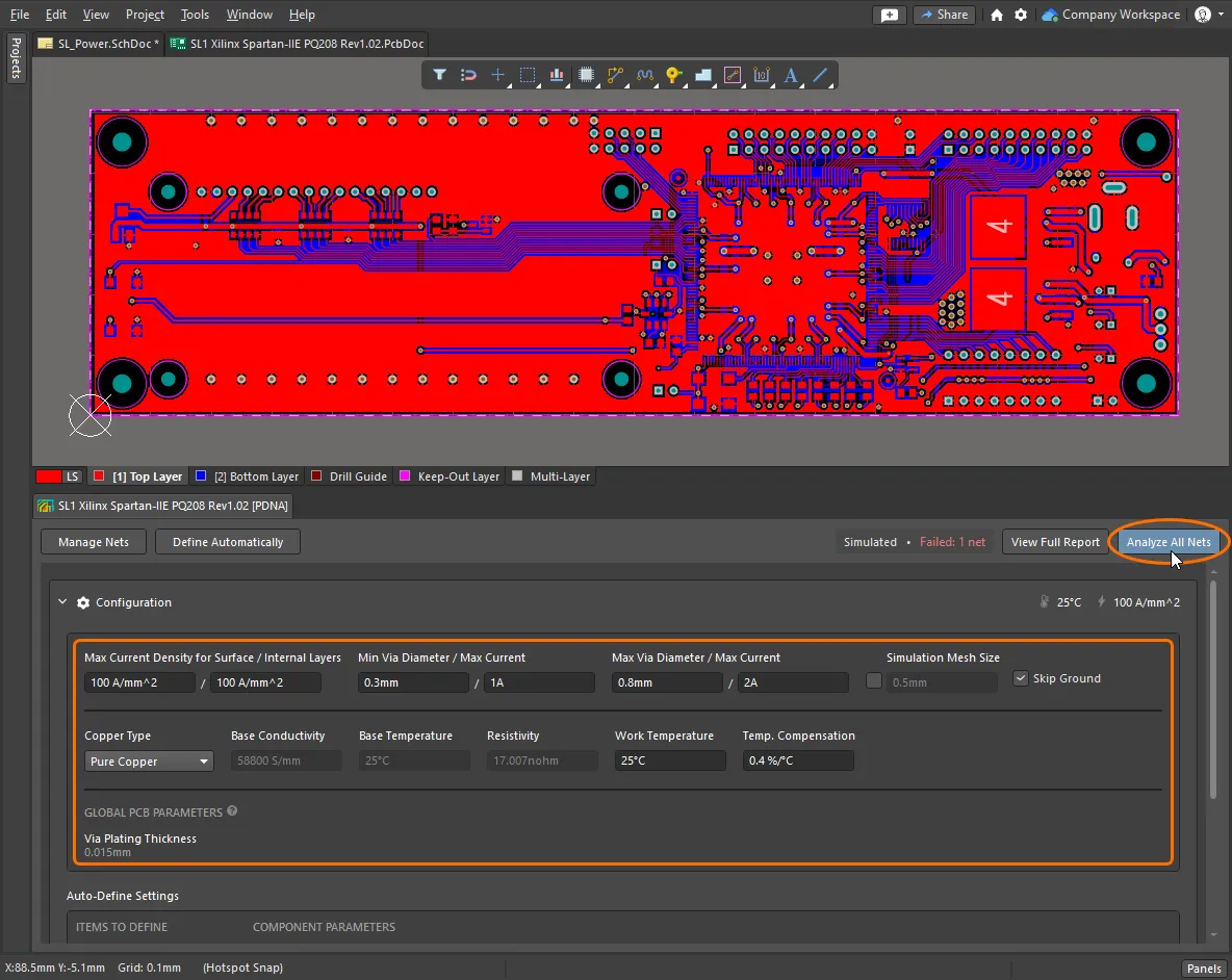
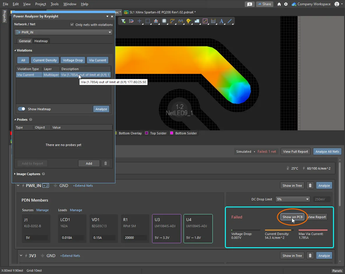
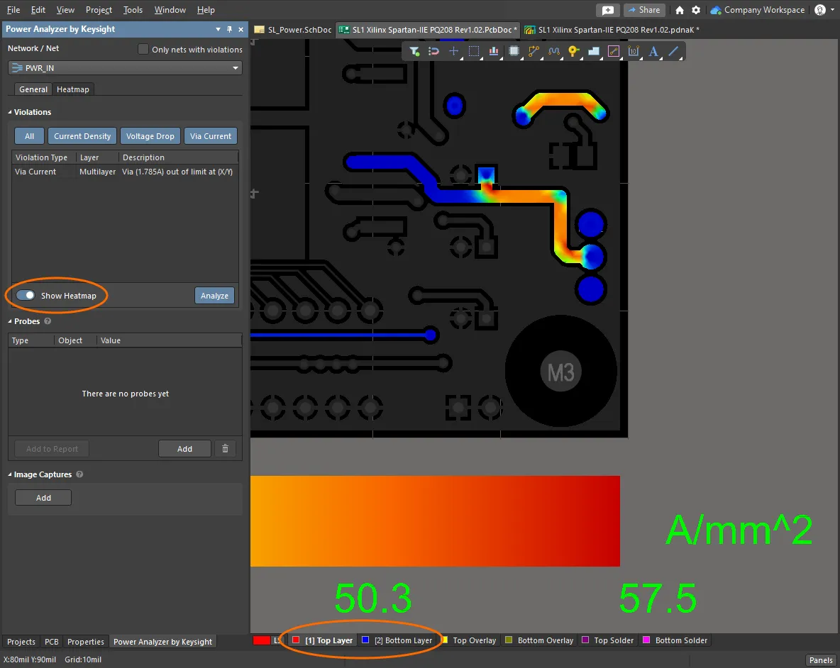
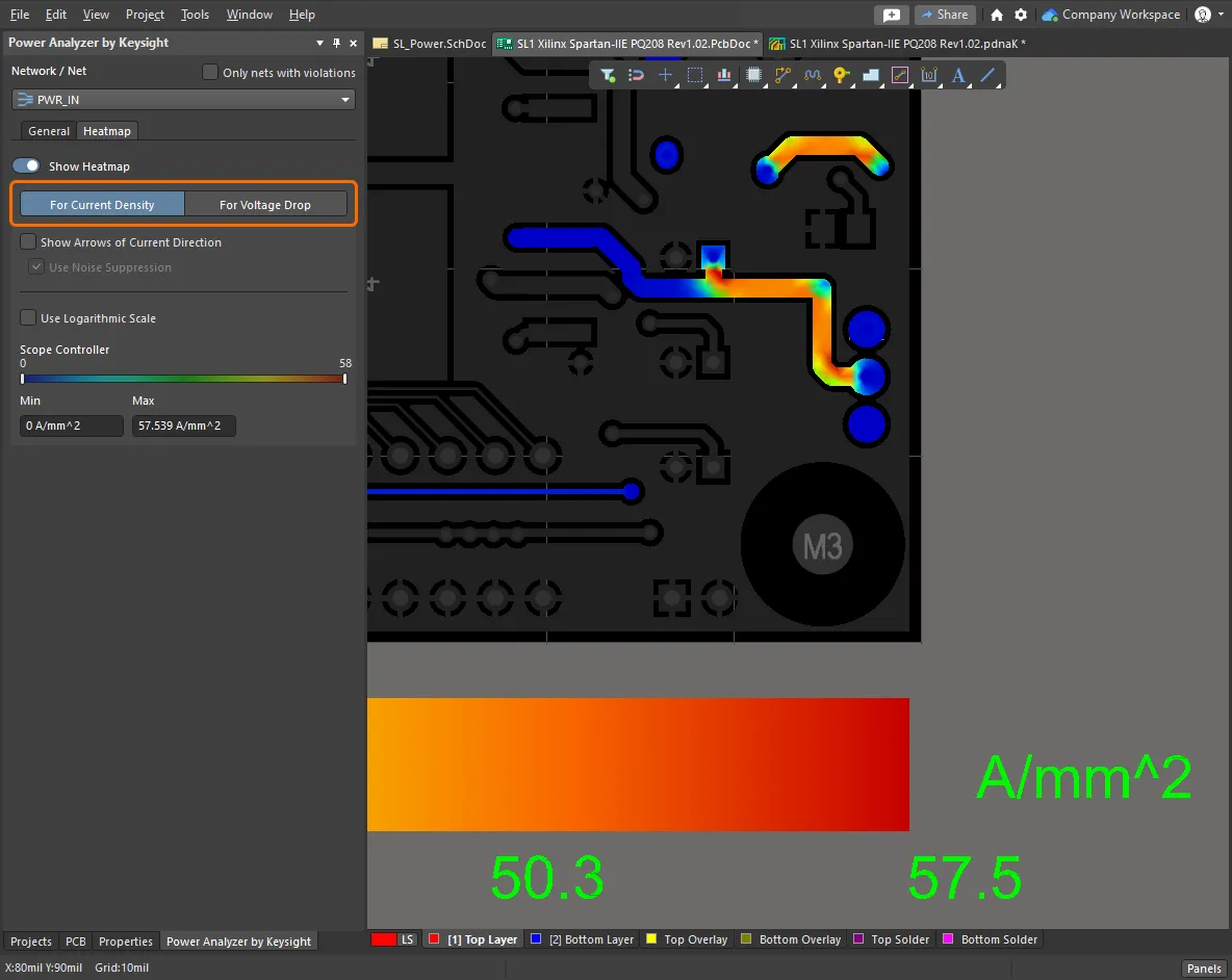
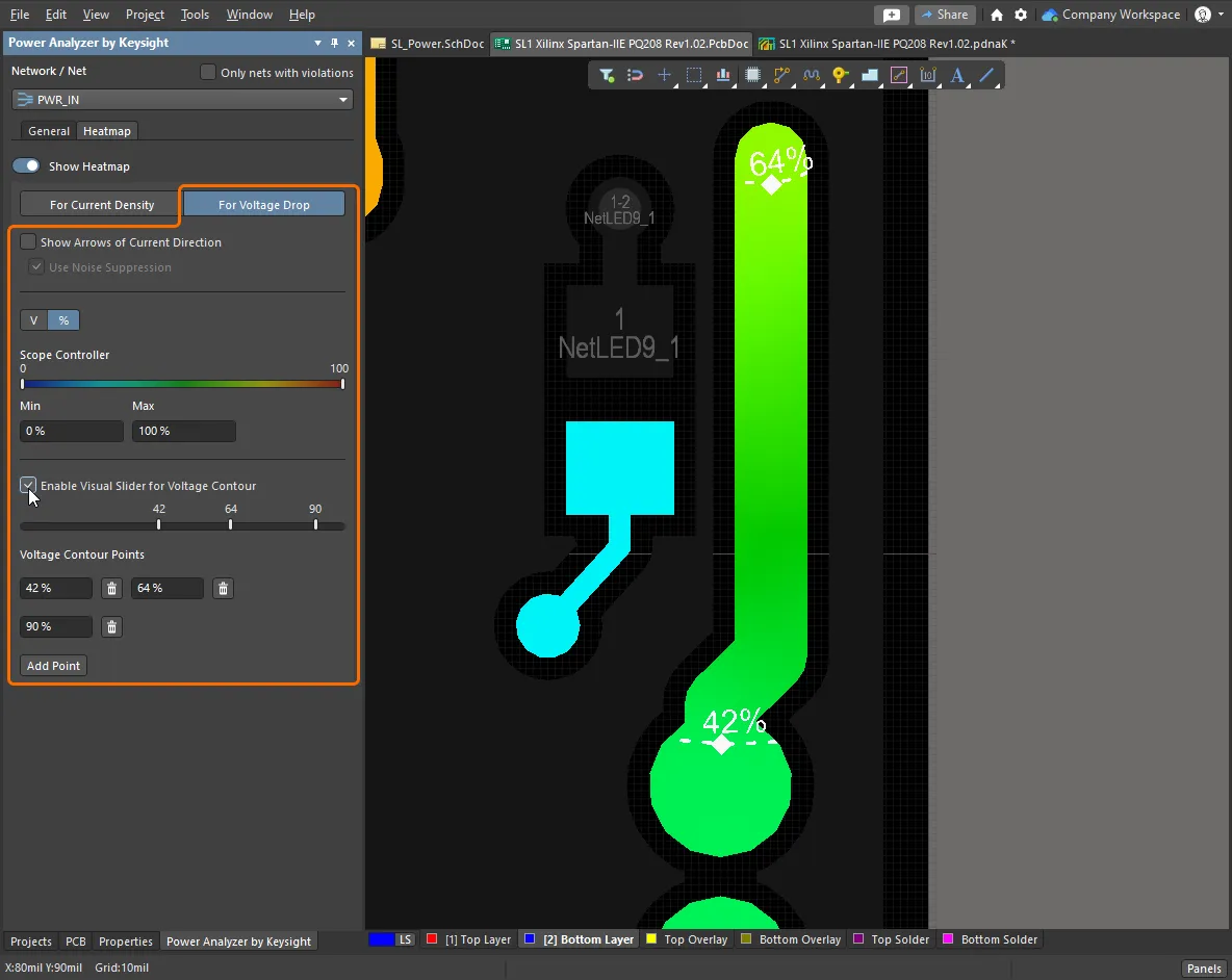
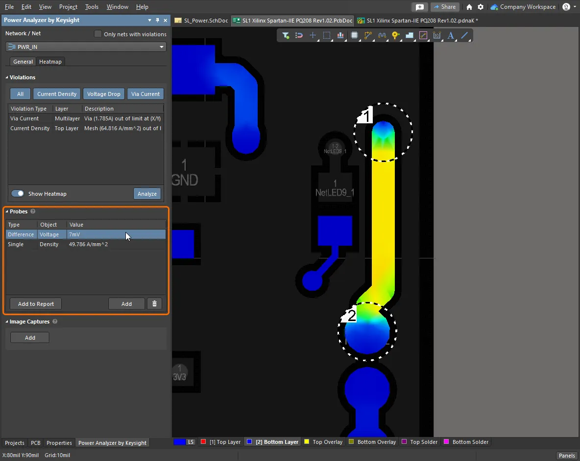
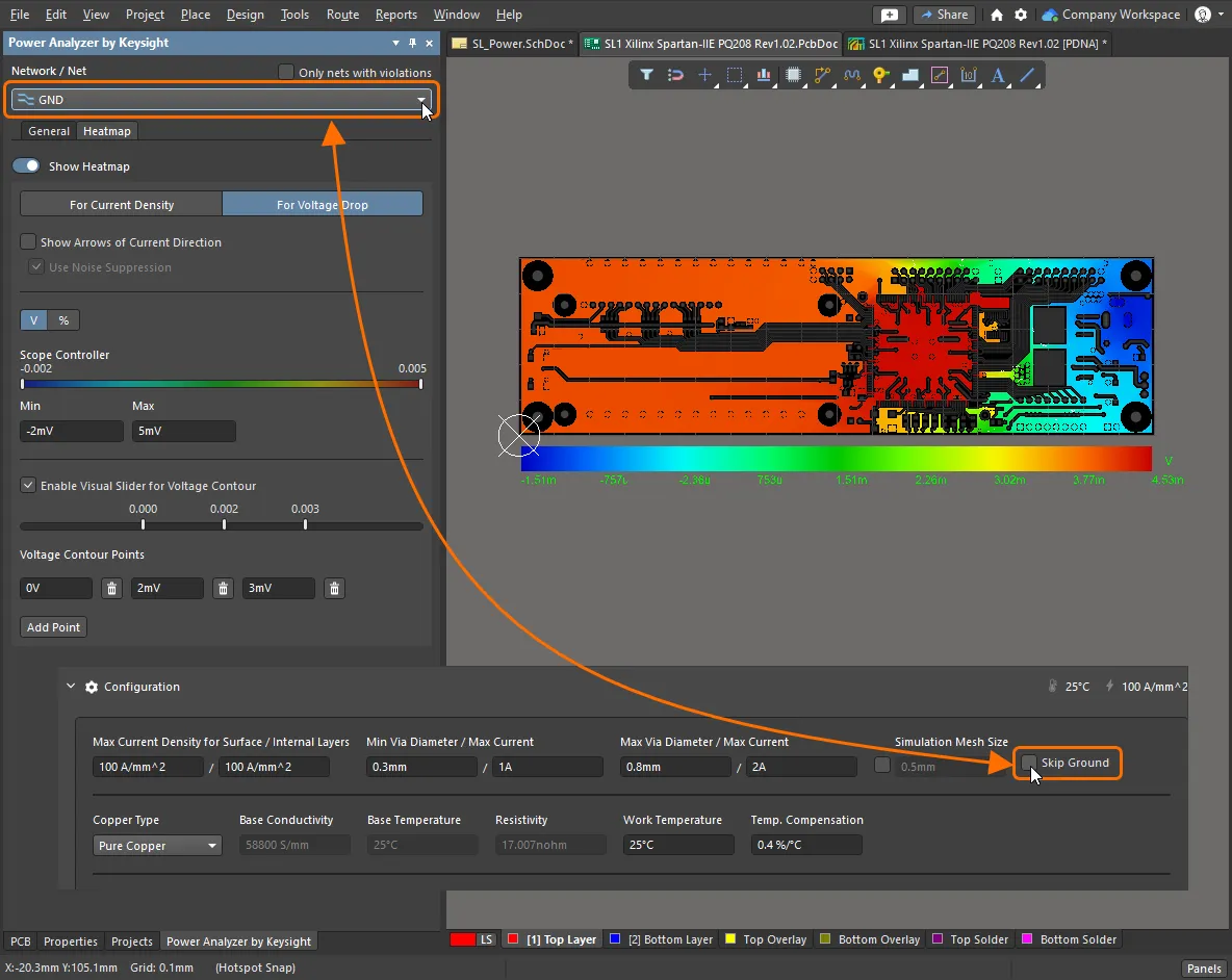
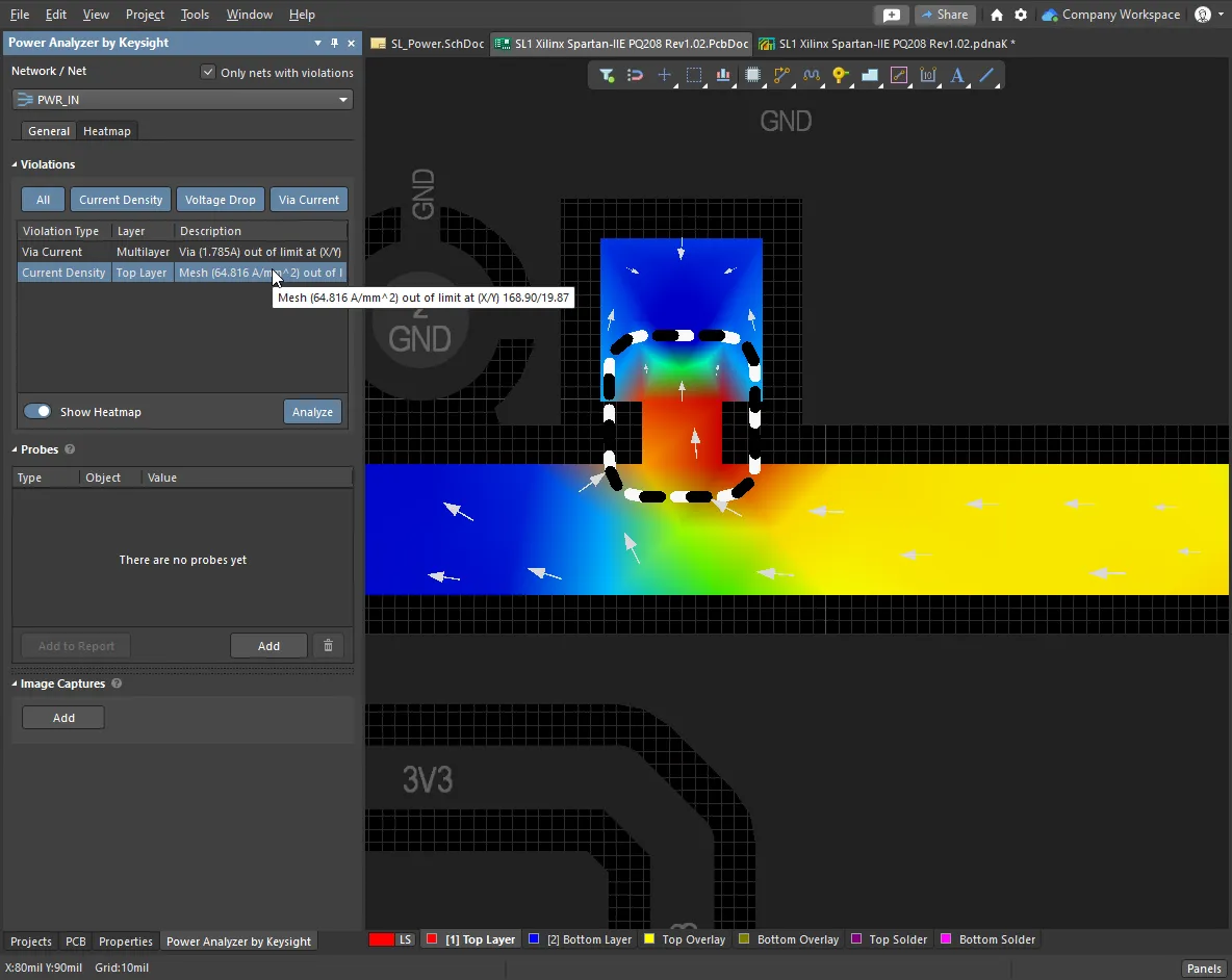
分析铜结构基于配置设置,当你点击 在 PCB 上显示Voltage Drop、Current Density 和 Max Via Current 的分析结果摘要会作为 检查热力图计算得到的电流流动与压降会以热力图形式直接显示在 PCB 编辑器中。使用 PCB 编辑器的层标签查看各层热力图,使用标准快捷键 2 和 3 在 2D 与 3D PCB 视图模式间切换,并在 Power Analyzer by Keysight 面板中点击 Show Heatmap 按钮,在电源分析热力图与标准 PCB 显示模式之间切换。 查看分析结果在 PCB 编辑器中,你正在查看的电源网络分析结果由 Power Analyzer by Keysight 面板控制。在面板顶部,选择要显示热力图的电源网络/网络(net)。注意:如果设计中存在违规项,默认会在下拉列表中包含 Only nets with violations;清除该选项即可在列表中包含所有电源网络。了解更多:Power Analyzer by Keysight Panel。 在电流密度与压降之间切换热力图会显示铜箔穿过方向的 Current Density,或沿着铜箔方向的 Voltage Drop;请使用面板中 Heatmap 选项卡顶部的按钮选择所需模式。板子下方会显示热力图的标尺,并会根据电流从 Zero 自动缩放到 Max Current Density,或根据压降从(Voltage - VDrop)自动缩放到 Voltage。热力图上还可以显示指示电流流向的方向箭头,并且可调整电流密度或压降的标尺。了解更多关于 配置与控制热力图显示 的内容。 探索压降电流密度热点的位置可以通过热力图上的颜色直接识别。由于压降是以位置之间的差值计算的,因此理解压降需要更深入的解读。为帮助识别关键位置,可使用 Enable Visual Slider for Voltage Contour 选项显示预定义的等值线,可按电压值或按百分比显示。了解更多关于 用于压降的热力图。 探测结果要直接从热力图上进行测量,请放置一个探针(Probe)。放置单个探针可显示该位置的绝对电流或电压;或在第二个位置单击,以测量两个探针点之间的差值。测量类型(V 或 I)由当前热力图模式(电流密度或压降)决定。请注意,探测通孔的中心点将始终显示电流密度。了解更多关于 探针。 检查地网结果默认情况下,地网(Ground net)会从热力图结果中排除。要将其包含在内,请在 |

解读与报告结果
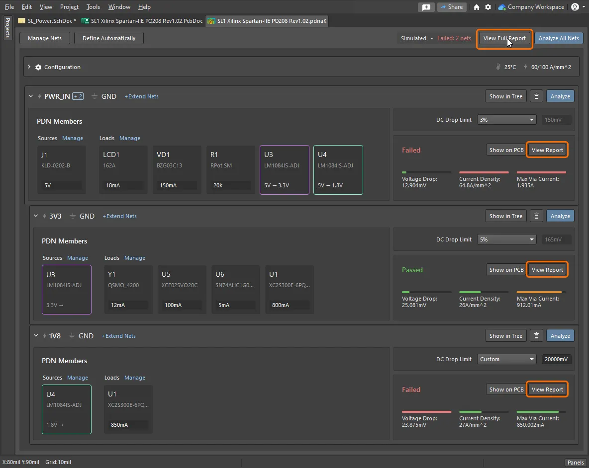
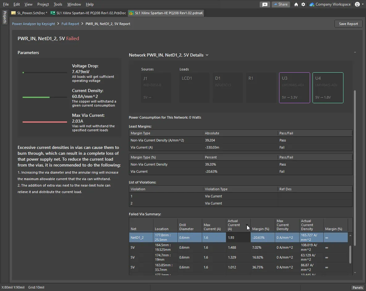
Power Analyzer 会在 PCB 编辑器中直接提供详细反馈。在 Power Analyzer by Keysight 面板中,可以快速调查违规项、放置测量探针,并将热力图捕获为图像。要访问板卡直流电源分析的详细信息,可以生成报告。详细报告会在 pdnaK 文档中打开,并可在其中将所需章节保存为 HTML 报告文件。报告既可以针对单个电源网络,也可以覆盖整个电源网络。
使用交互式图形结果在交互式 Power Analyzer by Keysight 面板中工作时,你可以快速识别并检查违规项。 生成报告要生成详细报告,请在 Power Analyzer by Keysight 文档( 详细网络报告 - 参数完整报告会列出所有已分析的电源网络;单击某个网络名称即可打开该网络的详细报告。网络报告左侧列出:
详细网络报告 - 结果报告右侧包含可折叠的章节:
详细网络报告 - 网络详情使用 Network Details 部分可快速识别设计中的潜在问题。该部分列出:
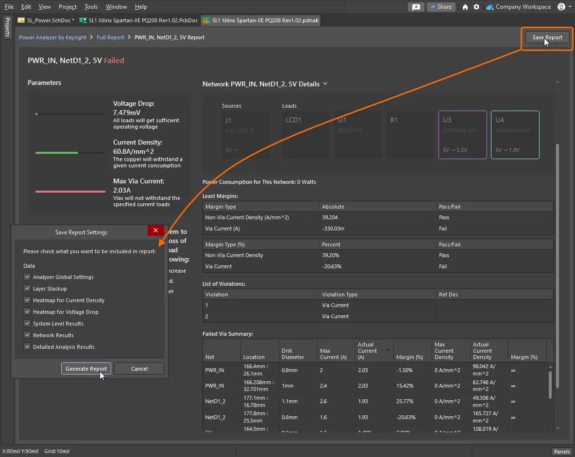
保存报告要创建分析的 HTML 报告,请单击
包含探针结果与图像捕获通过 Power Analyzer by Keysight 面板中的 |
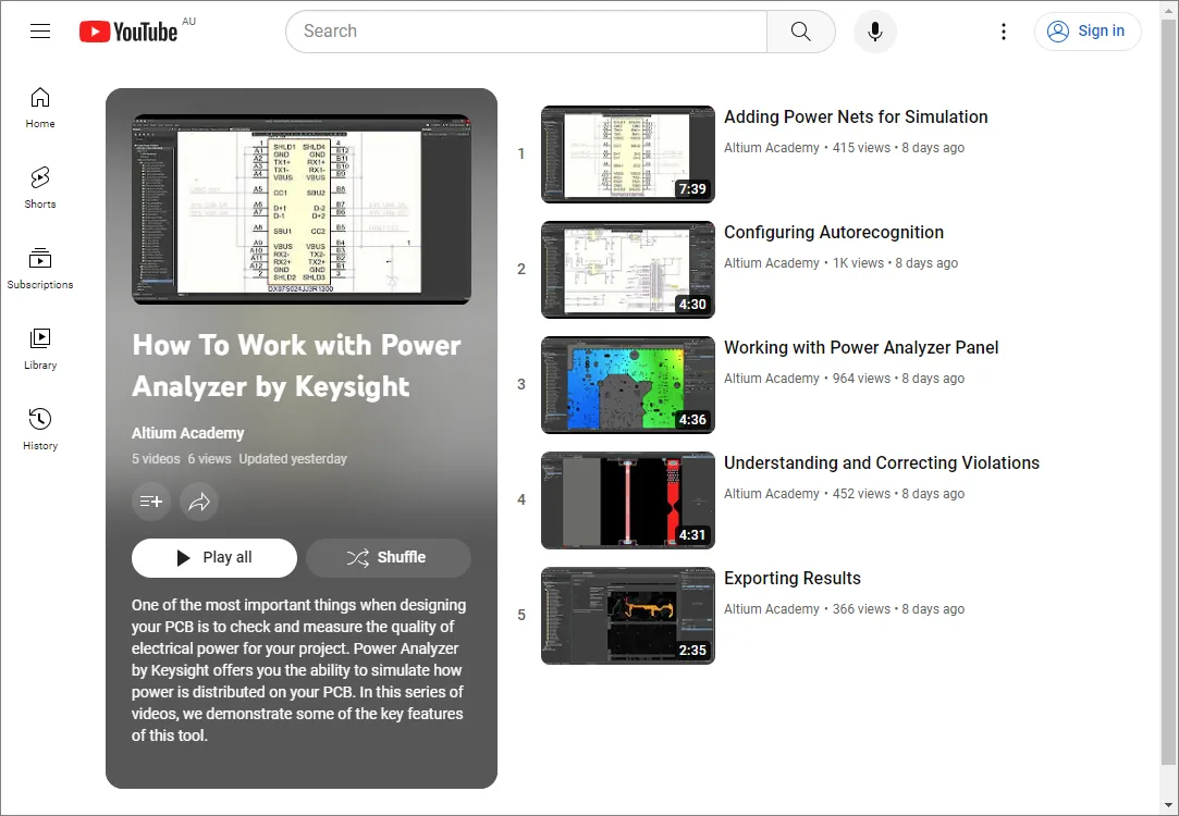
播放列表 - 如何使用 Power Analyzer by Keysight
学习如何使用新的设计软件需要时间。如果你更适合通过观看来学习,不妨查看这个视频播放列表,它演示了 How to Work with Power Analyzer by Keysight 的一些关键功能。
 AI 翻译
AI 翻译