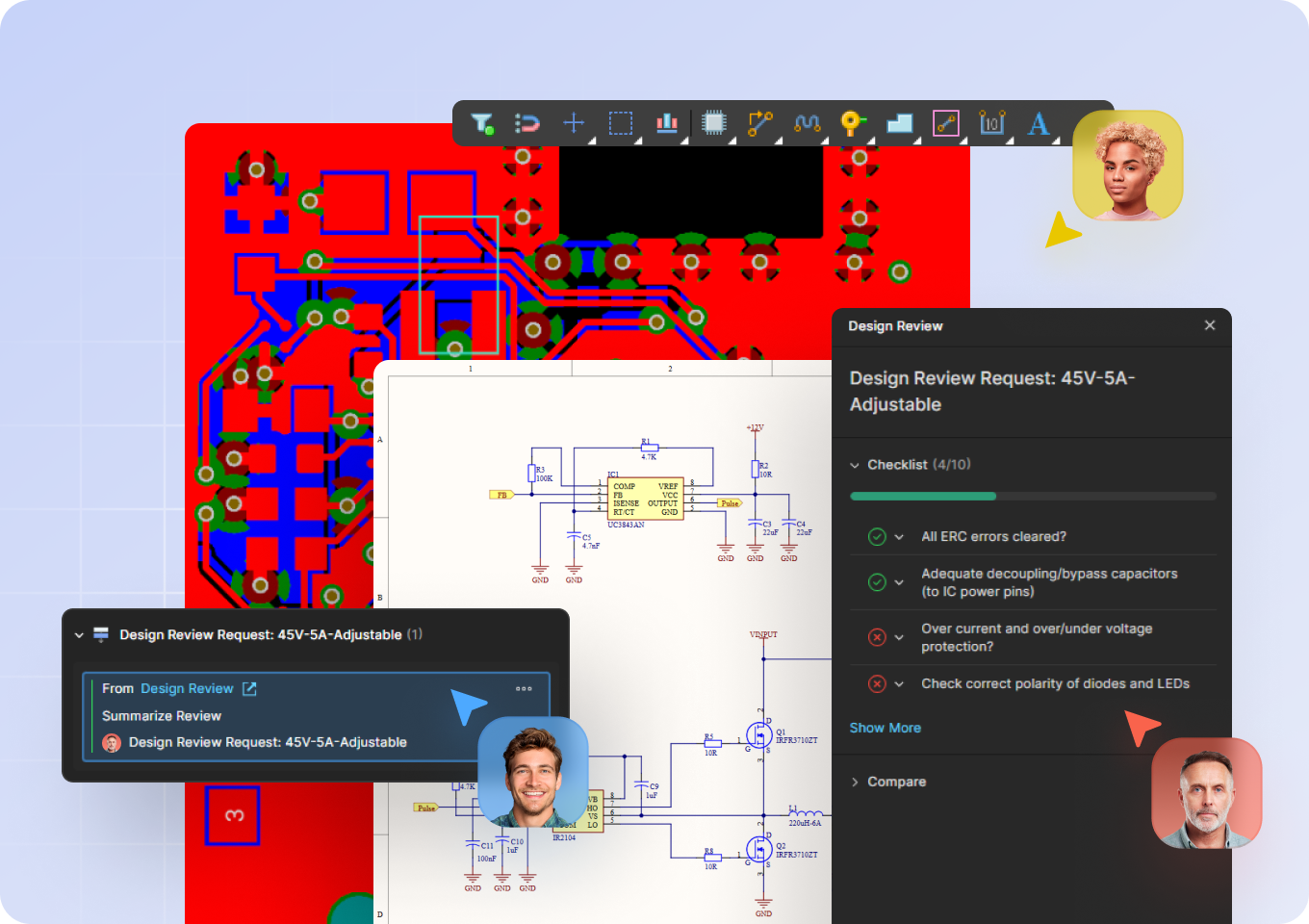
Professional PCB Design Review
Review every detail of a PCB design with full visibility into layers, rules, stack-up, and connectivity.
Understand how a board is built without disrupting the original design.
Start Reviewing Fast
Unified design puts schematic, layout, rules, and outputs in one place. You get a professional environment that’s easy to pick up and built to quickly understand how a board is designed.
Complex Design Made Simple
Design rules, stack-up, sourcing data, and verification details are visible together. You get the visibility needed to quickly understand how a board is structured.
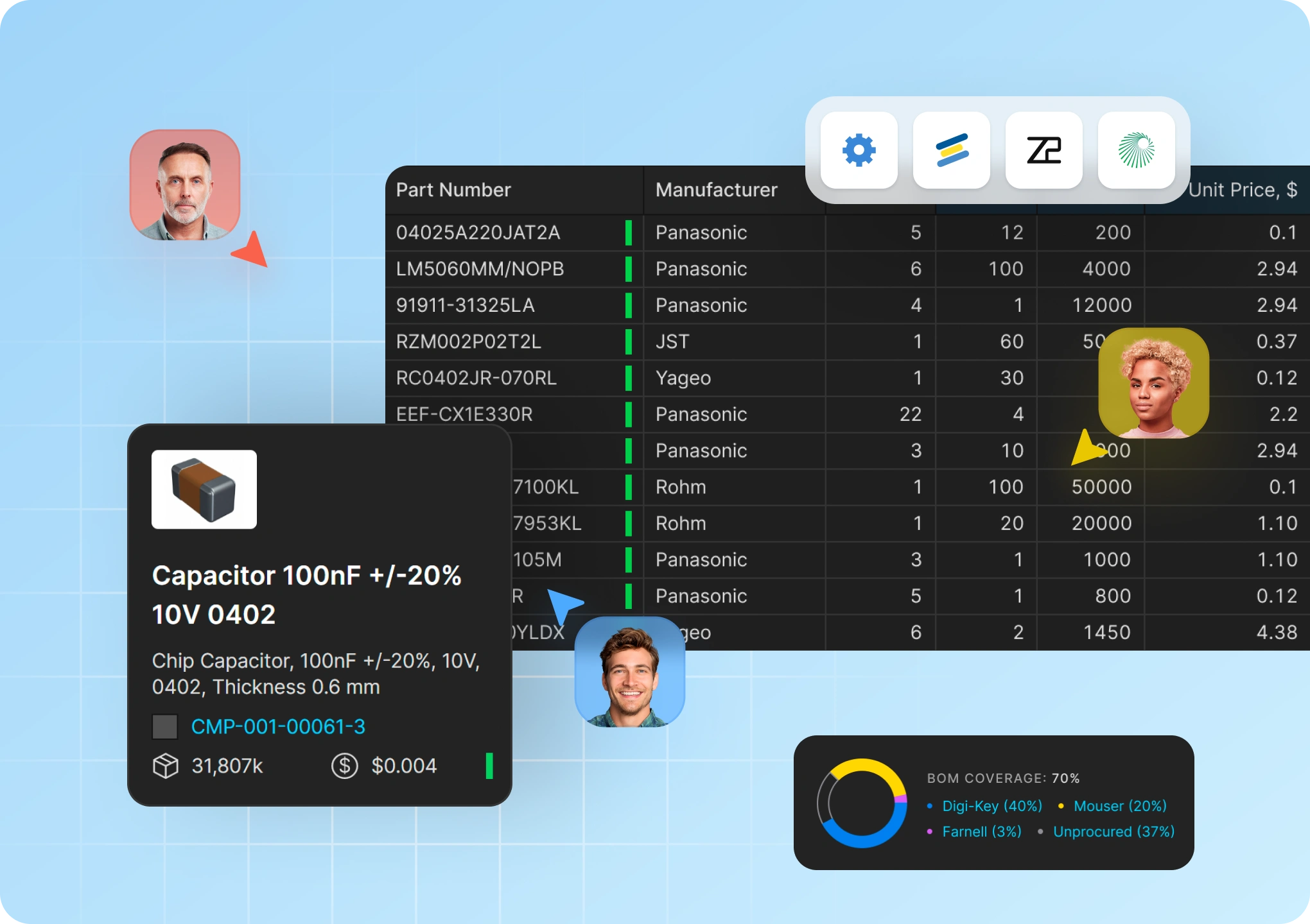
Your Complete PCB Design Toolkit
Schematic capture, PCB layout, active BOM, and manufacturer parts come together in a complete PCB design kit trusted by engineers. You get everything needed to see how boards are built from concept to production with the gold standard for PCB design.
Key Capabilities
Explore the designer-first capabilities of Altium Develop
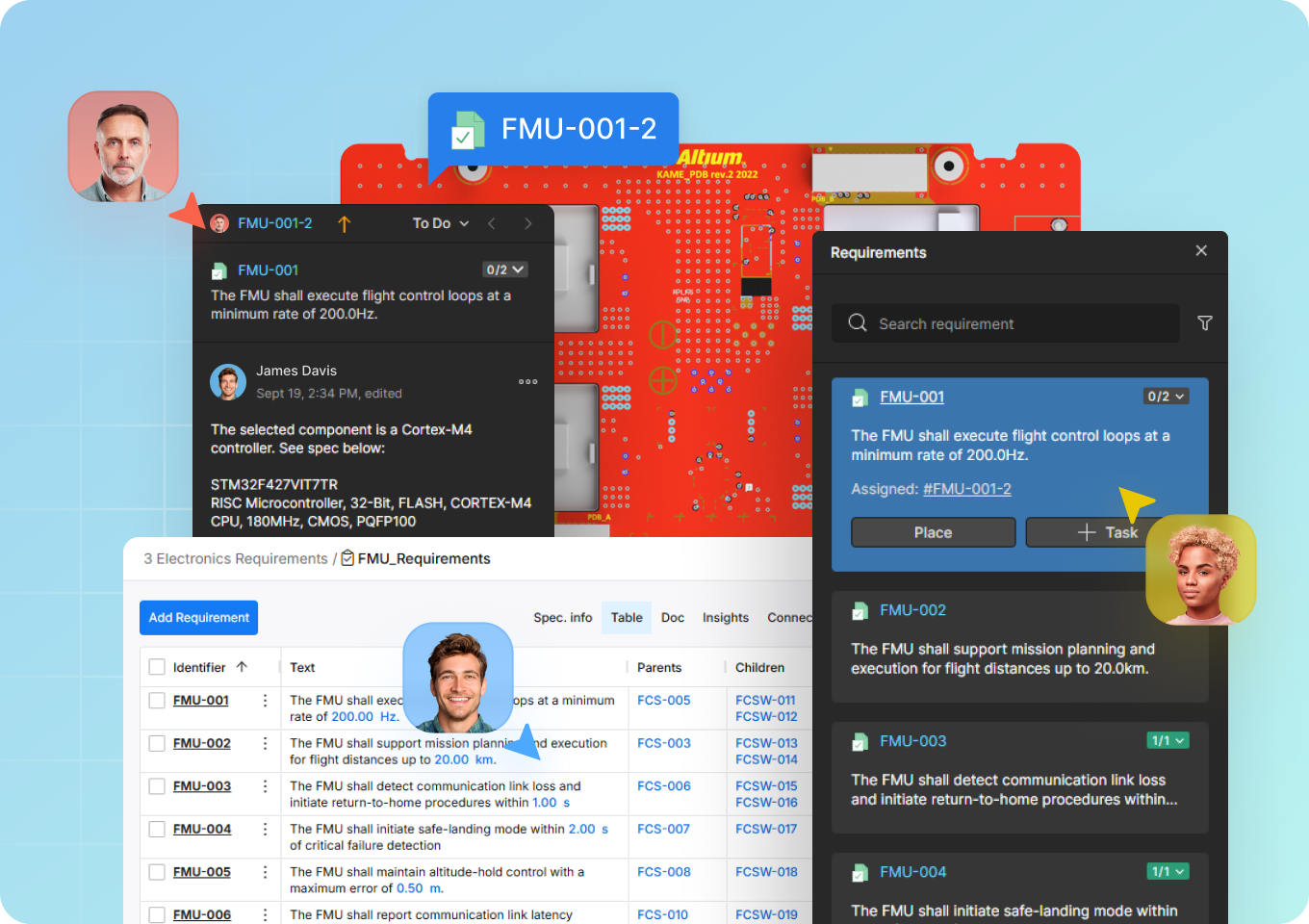
Confident Change Without Breaking Design
Seamless workflows between schematic capture and PCB layout make it easy to review changes and understand how updates affect the design.
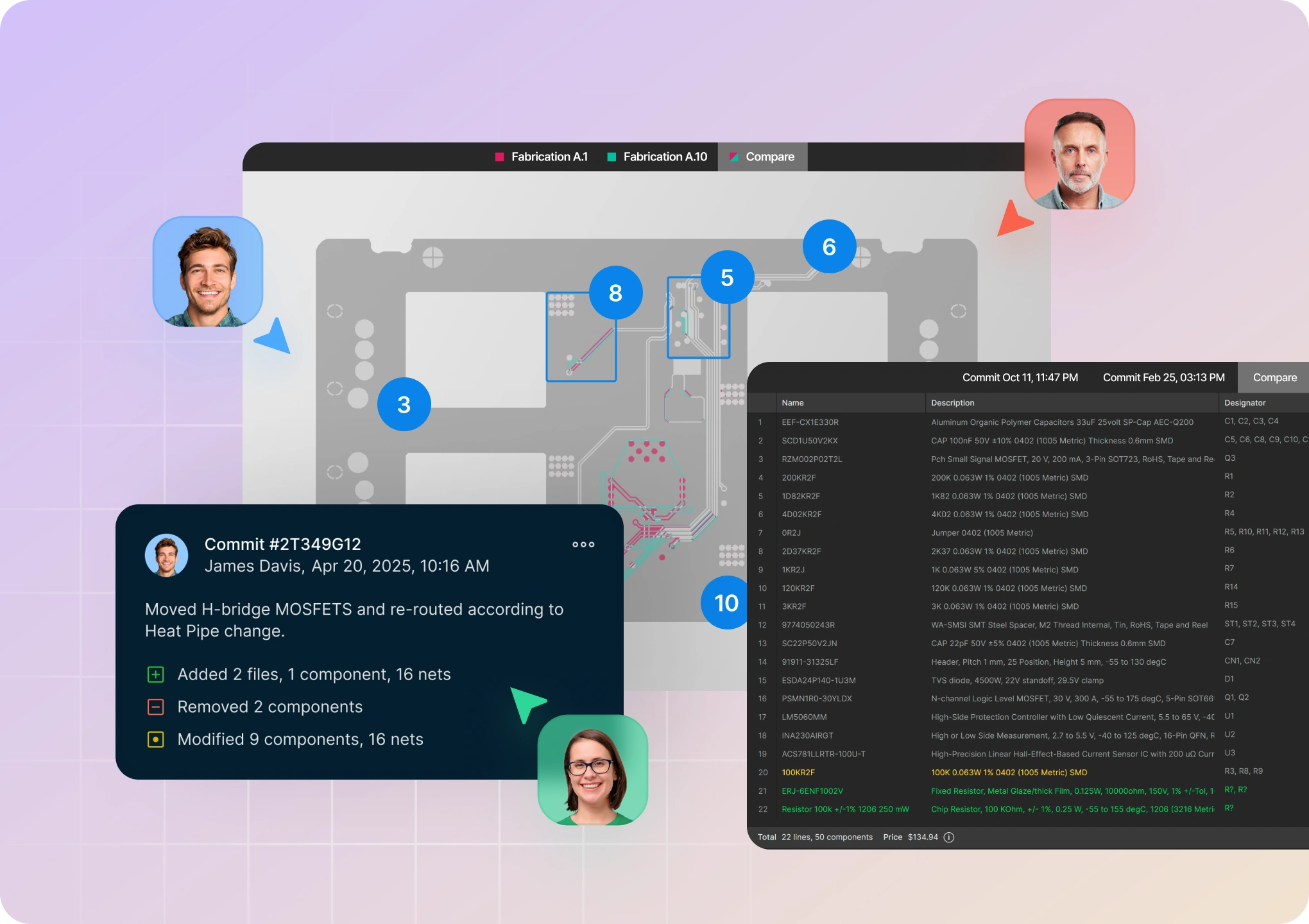
Professional Outputs Without Friction
View manufacturing files, drawings, 3D visualization, and release artifacts directly from the design environment. Everything you need to review what will actually be built.
System-Level Design Without Integration Surprises
Review connectivity across multiple boards with integrated harness workflows and system-level checks that help identify potential integration issues early.
Flexible Support Without Mandates
Access built-in version clarity, contextual design reviews, and secure sharing when needed—reducing version confusion and stress without changing how you work.
Valued by Users,
Trusted by Organizations

Electrical Engineering Manager at CAPEMC
“The best thing about this software is that it is a complete suite that includes Circuit simulator, Schematic Capture, PCB designer, MCAD for 3D modeling, and many more functions required for an electronics design process. The best thing about this software is that it is the oldest EDA suite therefore, it has the largest component library covering every electronic part and a lot of help is available for this software online.”

Sr. Printed Circuit Board Designer at Nikola Motor Company
“Altium Develop is the most progressive ECAD design tool out there! Altium is always making improvements [...] and has definitely saved our company money by increasing our efficiency in our board design efforts.”

Electrical Engineer at Overwatch Imaging
“Altium Develop is a continually improving, well-developed powerhouse. I like the thorough integration of its functionalities. Automation of many otherwise error-prone tasks. Keeps up with constant changes in design requirements.”


Get Started
with Altium Develop
Experience Unlimited Power
Risk Free for 30 Days