Orcad and PADS Designs and Libraries Files
Selecting the OrCAD and PADS Design Files
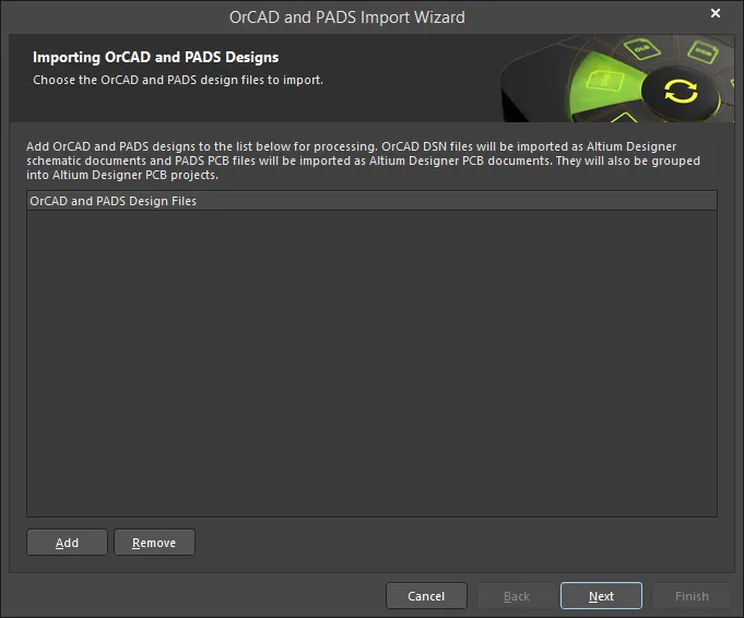
Use this page of the Wizard to add the OrCAD and PADS design files you want to import. Click Add to search for and select the desired files. Click Remove to delete a selected file.
Selecting the OrCAD and PADS Library Files
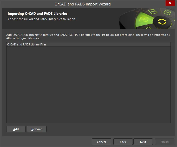
Use this page of the Wizard to add the OrCAD and PADS library files you want to import. Click Add to search for and select the desired files. Click Remove to delete a selected file.
Setting the Reporting Options
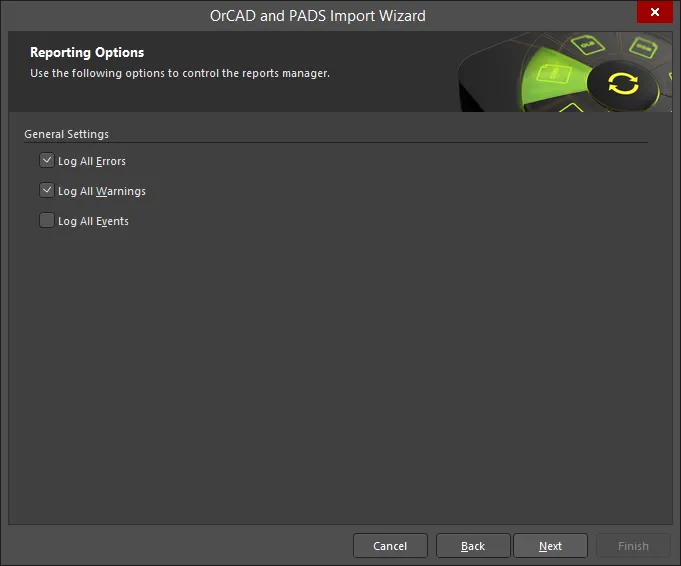
Use the Reporting Options page to set up general log reporting options.
Under General Settings, enable the desired options: Log All Errors, Log All Warnings, and Log All Events.
Setting the Schematic Options
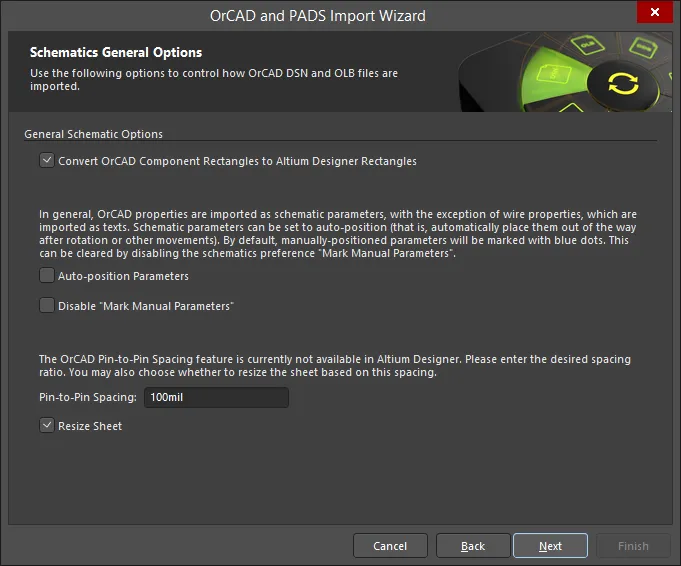
Use this page of the Wizard to control how OrCAD DSN (design) and OLB (library) files are imported.
Enable Convert OrCAD Component Rectangles to Altium Designer Rectangles if desired.
Usually, OrCAD properties are imported as schematic parameters (with the exception of wire properties) and are imported as texts. Schematic parameters can be set to auto-position by enabling Auto-position Parameters, which will automatically place them out of the way after rotation or other movements. By default, manually-positioned parameters will be marked with blue dots. To disable this default, enable Disable "Mark Manual Parameters".
The OrCAD pin-to-pin spacing feature currently is not available in Altium Designer. Enter the desired spacing ratio in the Pin-to-Pin Spacing textbox. If you want to also resize the sheet based on the entered spacing, enable Resize Sheet.
Setting Schematic Sheet Options

Use this page of the Wizard to control how OrCAD pages and junctions are imported.
OrCAD title blocks are imported as schematic components. Altium Designer also supports this feature; however, the title blocks in Altium Designer are limited to two types: Standard and ANSI and their graphics are not editable. If this is not desirable for your situation, templates can be used to provide a more flexible solution. Templates allow any graphical data to be placed onto a schematic sheet. Enable Strip OrCAD Title Blocks to strip the OrCAD title blocks. Check Enable Schematic Title Blocks if desired, then use the drop-down to select Standard or ANSI.
Enable the Force convert all I/O and Bi-directional pins to passive pins to automatically convert to I/O and bi-directional pins to passive pins.
Setting PCB and PCB Library Default Options
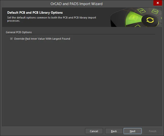
Use this page of the Wizard to set default options that are common to both the PCB and PCB Library import process.
Enable Override Pad Inner Value With Largest Found to specify that imported pads will have their sizes on the mid-layers set to the largest size found.
Setting Options for PCB Import Process
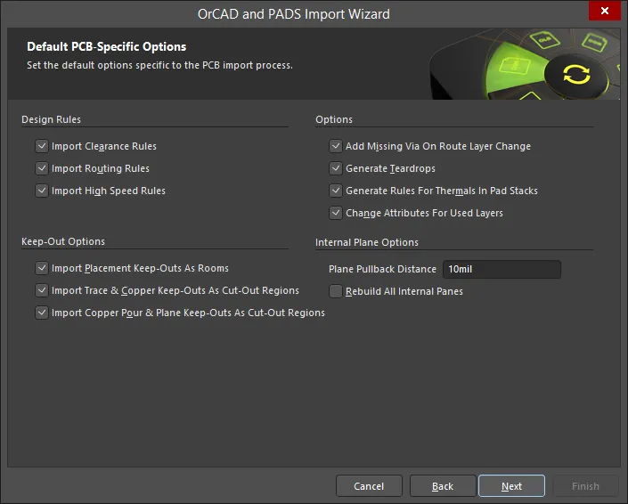
Use this page of the Wizard to set default options that are specific to the PCB import process.
Enable any Design Rules you want to import: Import Clearance Rules, Import Routing Rules, and Import Routing Rules.
Enable any Keep-Out Options you want to import: Import Placement Keep-Outs As Rooms, Import Trace & Copper Keep-Outs As Cut-Out Regions, and Import Copper Pour & Plane Keep-Outs As Cut-Out Regions.
Enable any desired miscellaneous Options:
-
Add Missing Via On Route Layer Change
-
Generate Teardrops
-
Generate Rules For Thermals In Pad Stacks
-
Change Attributes For Used Layers
Specify the desired Plane Pullback Distance in the textbox. Enable the checkbox to Rebuild All Internal Planes.
PCB and PCB Library Options

This page of the Wizard is used to review and edit options for each PADS PCB and PCB Library. Any unmapped layers are highlighted in pink.
Click Edit Mapping to open the PADS PCB Library ASCII File Import Options dialog.

All used PADS PCB layers must be mapped to an Altium Designer layer prior to import. The PADS PCB Library ASCII File Import Options dialog allows the user to map PADS PCB layers to an Altium Designer layer. The dialog also gives access to the Importer Settings dialog in which the user can control design rules, missing vias and keep-out conversions during the import process.
Setting Output Library Options
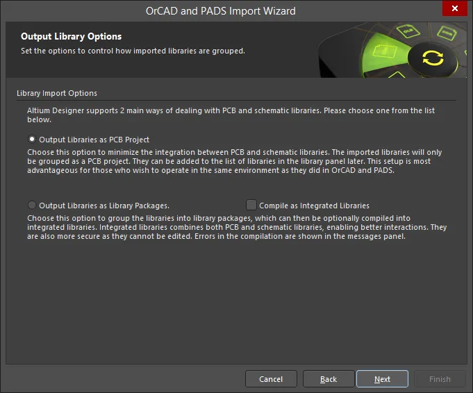
Use this page of the Wizard to control how the imported libraries are grouped.
Library Import Options – select one of the following options for how to group output libraries.
-
Output Libraries as PCB Project – select to minimize the integration between PCB and schematic libraries. The imported libraries will only be grouped as a PCB project. They can be added to the list of libraries in the library panel later. This setup is most advantageous for those who wish to operate in the same environment as they did in OrCAD.
-
Output Libraries as Library Packages – select to group the libraries into library packages. You can then select to compile the library packages as integrated libraries by enabling Compile as Integrated Libraries. Integrated libraries combine both PCB, schematic and PSpice libraries, enabling better interactions. Errors in the compilation are shown in the Messages panel.
Specifying the Output Directory

Use this page of the Wizard to review the output project structure and specify the output directory in which to import the files. Use the Browse Folder icon to search for and choose the Project Output Directory.
Click Menu to access options to edit the project structure:
Right-clicking in the PCB Projects region gives access to the same menus and sub-menus as clicking the Menu button.
Specifying the Output Library Directory

Use this page of the Wizard to review the output library structure and specify the output directory in which to import the library files. Use the Browse Folder icon to search for and choose the Library Output Directory.
Executing Import Process

This page shows a green progress bar of the import process.
Closing the Wizard
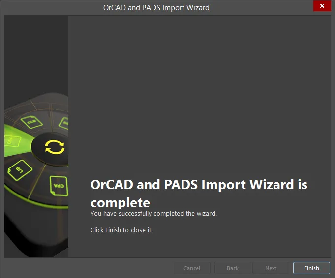
The OrCAD and PADS Import Wizard has completed. The Messages panel appears with any relevant messages. Click Finish to close the Wizard. If any warnings were generated during the import process, a *.LOG file opens showing the warnings.
PADS and OrCAD files translate as follows:
-
PADS ASCII PCB Layout (
*.ASC) files translate to Altium Designer PCB files (*.PcbDoc).
-
PADS ASCII PCB Library files translate into Altium Designer PCB library files (
*.PcbLib).
-
OrCAD Capture (
*.DSN) files translate to Altium Designer schematic files. Each page within a .DSN file will be imported as a single Altium Designer schematic file (*.SchDoc). Design caches within a .DSN file will be imported as a schematic library (*.SchLib). Design hierarchy is maintained, including complex hierarchy.
-
OrCAD schematic library (
*.OLB) files will be translated into Altium Designer schematic library files (*.SchLib).
-
The files will be grouped into an Altium Designer PCB project (
*.PrjPCB) that is automatically created.
-
Translated OrCAD libraries are automatically grouped into one PCB project.
