
KB: Custom pad shape
Solution Details
Custom Pad Shape Creation
Custom pad shapes are created by placing other design objects, such as arcs, fills, lines, or regions to build up the copper shape required for the pad. Placing a small Pad within the shape is required to define the connection point in the pad, and if required, the drill hole location and size.
Any design object can be used to build up the required copper shapes needed for the pads. Choose the object to suit the shape required. In this example, the use of a simple Solid Region is shown.
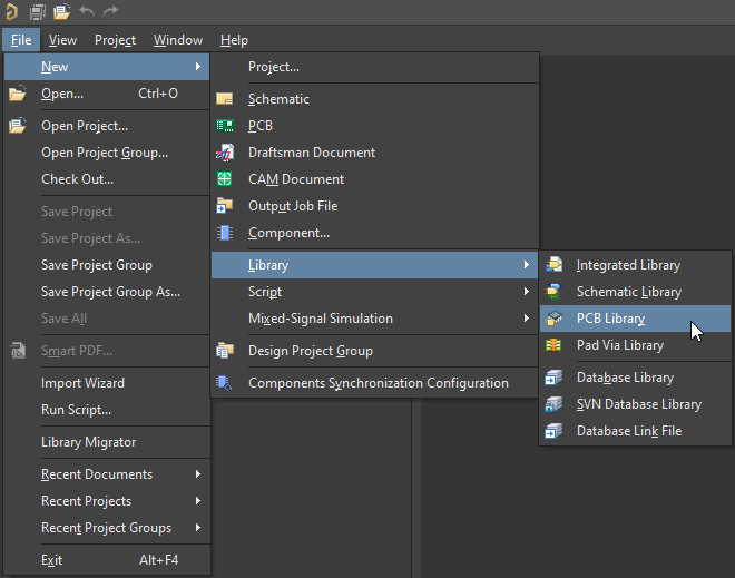
Within a .PcbLib Footprint Creation/Editing environment
File » New » Library » PCB Library
Place » Solid Region
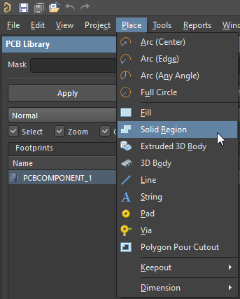
Create your custom shape using the these Tips:
- Press Shift+Spacebar to cycle through the corner modes
- Press Spacebar within each corner mode to toggle the corner direction (except for the Any Angle mode).
- Press Backspace to remove the last corner.
- Press Esc or Right-Mouse Click to terminate the placement process, the software will close and complete the Region.
- For the Arc Corner Modes, the Arc can be Resized using the ‘,’ and ‘.’ keys. Hold Shift to accelerate the re-sizing process.
Solder and Paste Mask
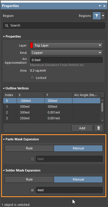
Any primitive object can have a calculated Solder and/or Paste Mask, which can either be a user-specified amount or controlled by the rule system. This is achieved enabling the appropriate Mask Expansion settings in the Properties panel when the primitive object is in selection, as shown in the image below.
Creating Connectivity
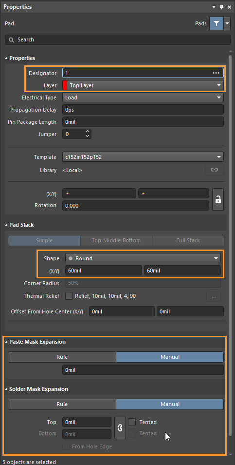
In order to create a Pin to Pad pad connection via Pin Designator in the schematic and define the connection point in the pad; a small pad must be placed into the region with the designator set accordingly to match the pin designator of the pin in the schematic symbol for which the footprint where the custom pad being used is attached.
Place » Pad » ‘Tab’
Set the properties of the Pad accordingly in the Properties Panel
In this case the Properties of the Pad are set to:
- Designator: 1
- Layer: Top
- Shape: Round
- (X/Y) 30mil
- Paste Mask Expansion: Manual - 0mil
- Solder Mask Expansion: Manual - 0mil
A Pad is placed in each section of the Region where there is need for Hotspot connection for Tracks and Spokes of a Thermal Relief. All pads in a footprint with the Designator of 1 will inherit the net assigned to the Pin with a Designator of 1 in the schematic symbol for which the footprint is attached to. To ensure the small pads are connected by spokes of a Thermal Relief connection, position them close to the edge of the custom shape so that the distance from the small pad edge to the edge of the custom shape is less than half the polygon connection spoke width.
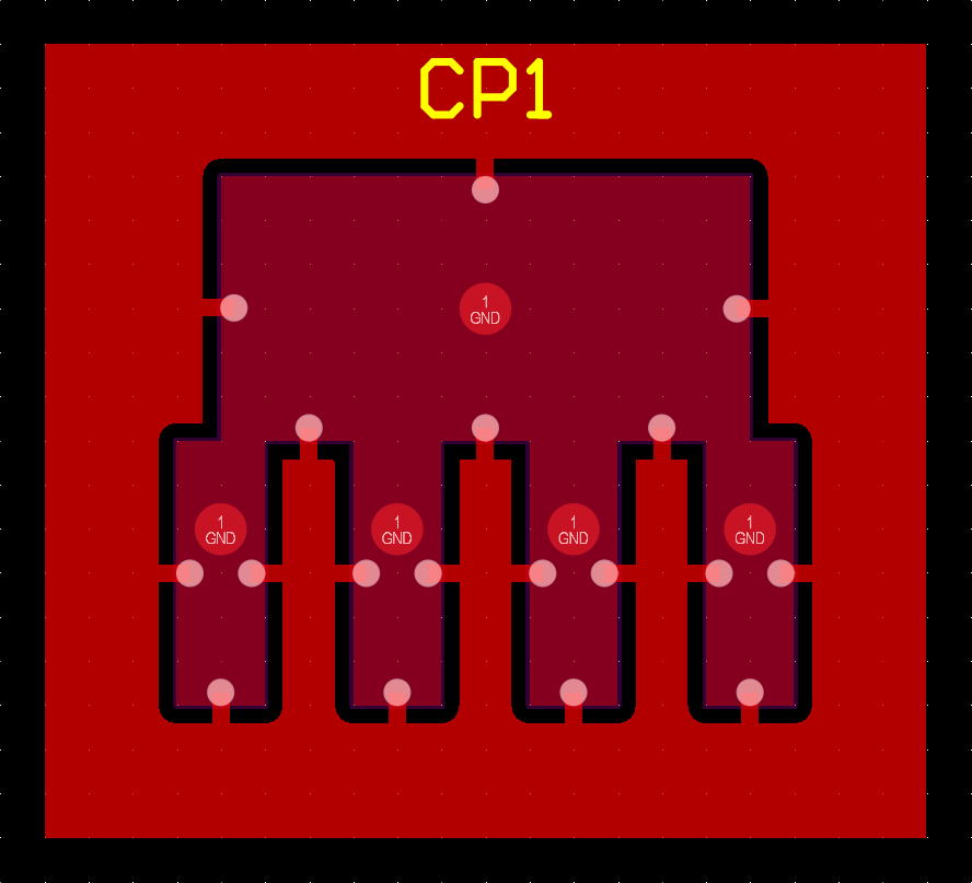
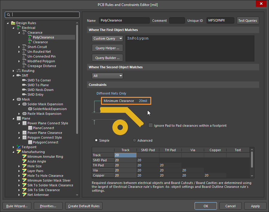
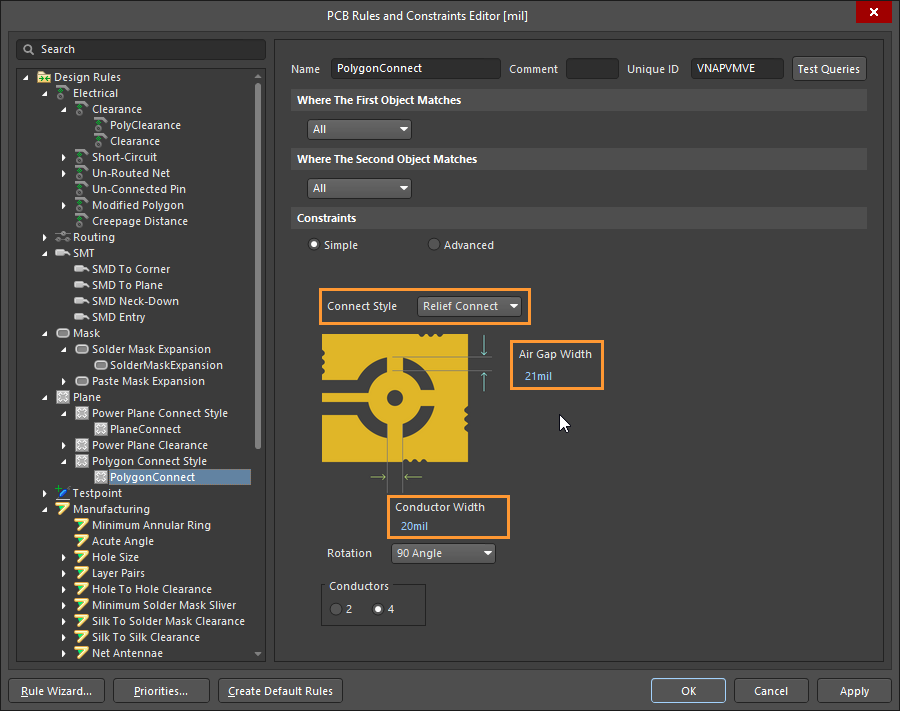
Ensure that your Clearance Rules set for Polygons matches the Conductor Width of the Polygon Connect Style Rule. In this example the Polygon Clearance is 20mils therefore the Polygon Connect Style Rule Conductor Width value is set to 20mils. Also it may be required to have the Air Gap Width value slightly larger to ensure connection.
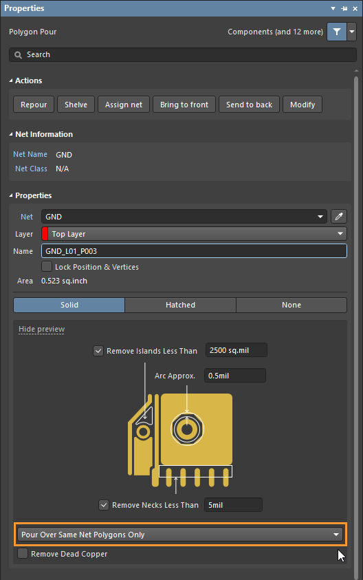
Properties of Polygons poured over custom pads that are having custom Thermal Relief connection points need to be set to Pour Over Same Net Polygons Only
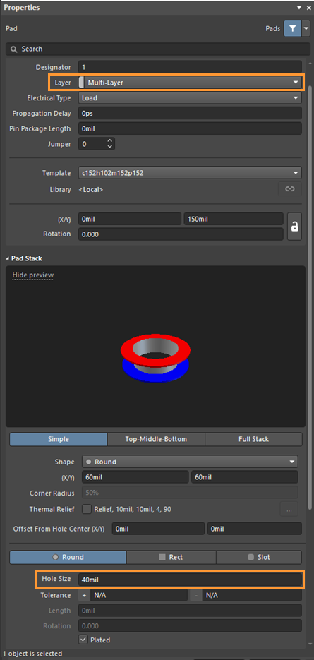
Drill Hole
If a Drill Hole is required; change the property of the internal pad to Multi-Layer and define the Hole Size accordingly in the Properties Panel.
As of writing, custom hole shape is not supported, while if non-plated thru-hole, a board cutout Region primitive can be leveraged instead.
See Also: