
Electrical Rule Types
Altium Essentials: PCB Design Rules Creation
This content is part of the official Altium Professional Training Program. For full courses, materials and certification, visit Altium Training.
At a Glance
- Learn how the Clearance rule defines spacing between PCB objects, including nets, differential pairs, pads, vias, holes, and copper features.
- See how to use the Minimum Clearance Matrix, Simple and Advanced modes, and editing shortcuts to create more targeted clearance rules.
- Understand special clearance cases such as same-net via to SMD pad checking, hole-to-object clearance, and layer-specific clearance behavior.
The design rules of the Electrical category are described below.

The Electrical category of design rules.
Learn more about Defining, Scoping & Managing PCB Design Rules.
Clearance
This rule defines the minimum clearance allowed between any two primitive objects on a copper layer. Either a single value for clearance can be specified, or different clearances for different object pairings, through use of a dedicated Minimum Clearance Matrix. The latter, in combination with rule-scoping, provides the flexibility to build a concise and targeted set of clearance rules to meet even the most stringent of clearance needs.
Constraints
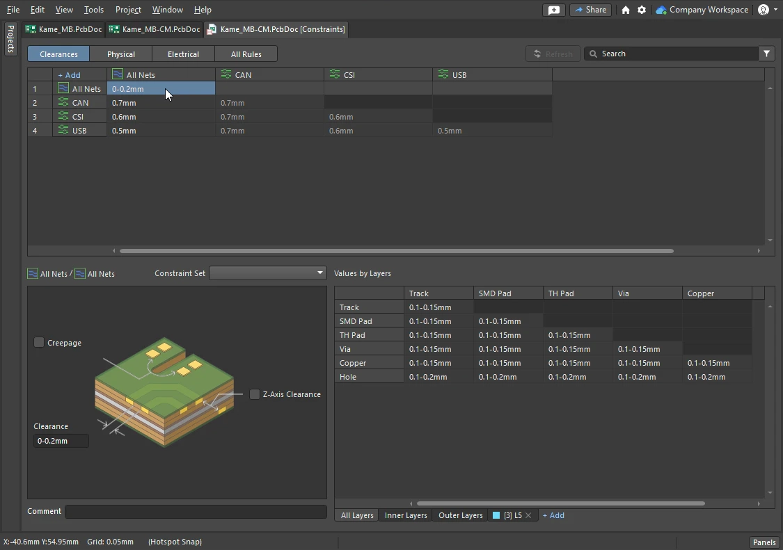
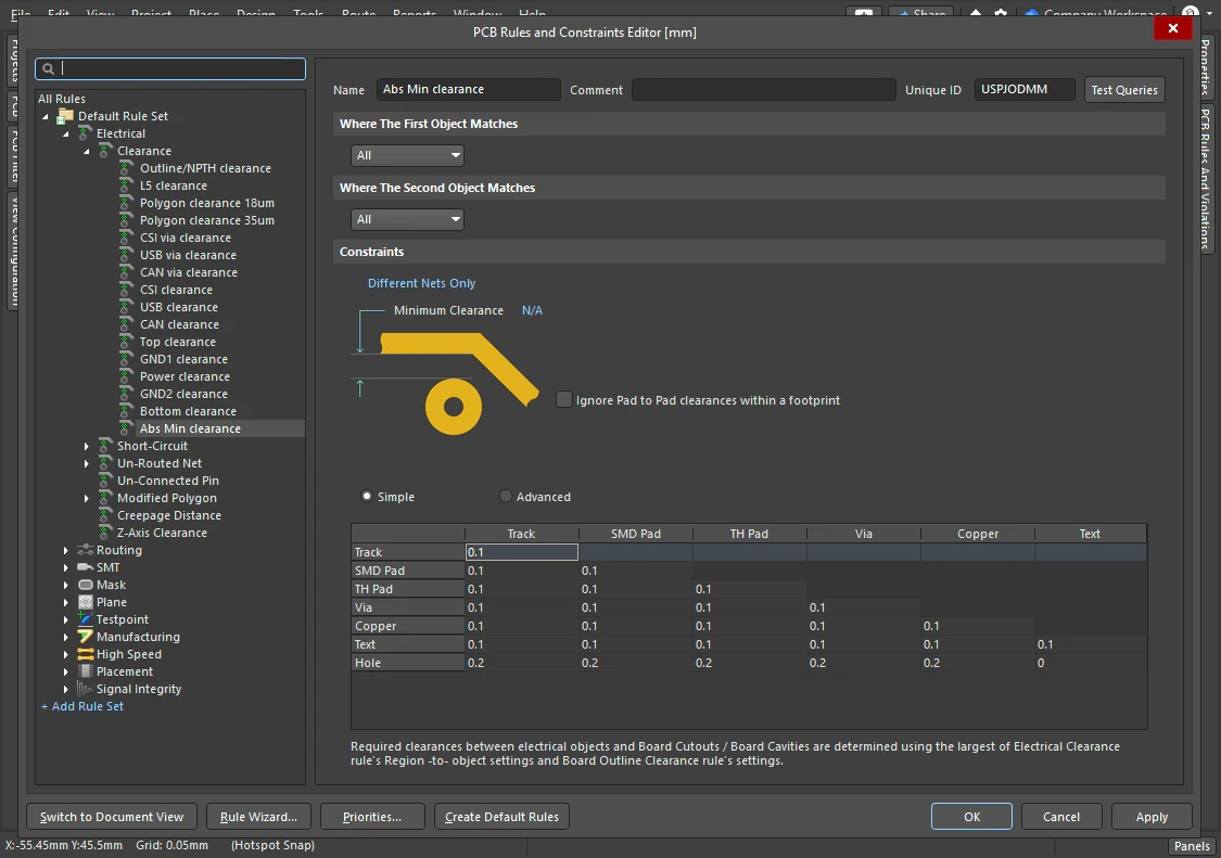
Clearance Constraint Settings
| Default Rule | Required |
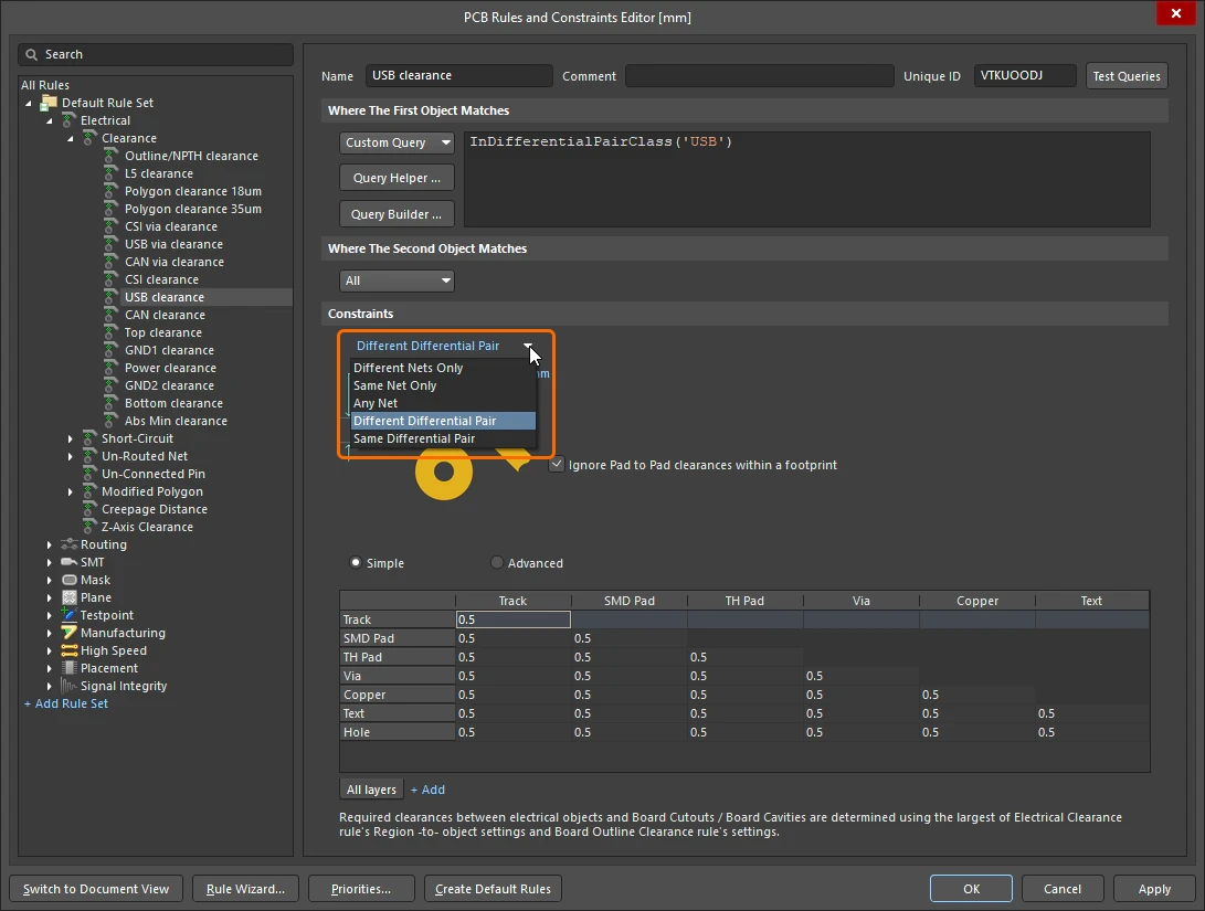
| Connective Checking | The set of net objects returned by the rule scope can be further narrowed down using the drop-down at the top of the Constraints region (
|
| Ignore Pad to Pad Clearances within a footprint | Toggle this option on/off to specify whether clearances between pads in the same component footprint are ignored. This option is disabled by default. |
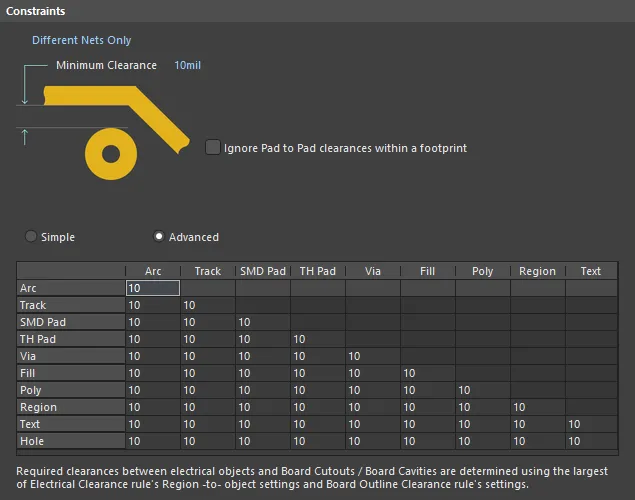
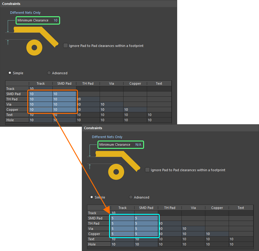
| Minimum Clearance | The value for the minimum clearance required. A value entered here will be replicated across all cells in the Minimum Clearance Matrix. Conversely, when a different clearance value is entered for one or more object pairings in the matrix, the Minimum Clearance constraint will change to N/A, to reflect that a single clearance value is not being applied across the board. |
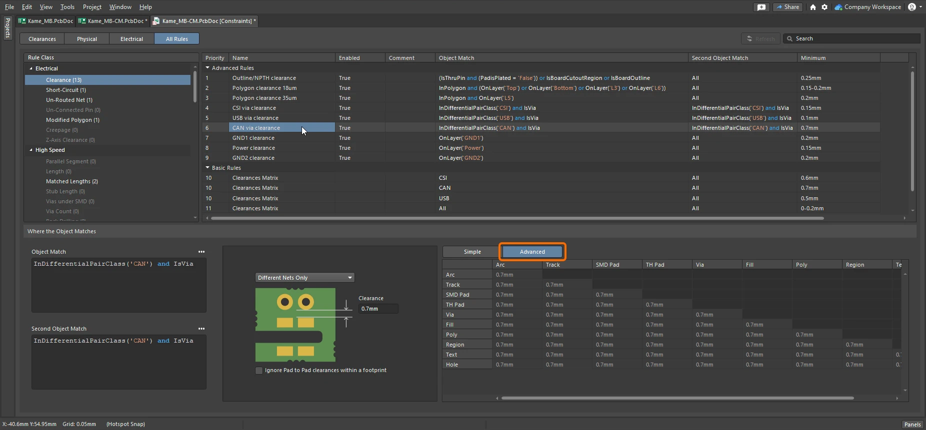
| Minimum Clearance Matrix | Provides the ability to fine-tune clearances between the various object-to-object clearance combinations in the design. |
| Simple/Advanced options | In the Minimum Clearance Matrix, the Simple mode is the default mode (
|
| Editing in the Clearance Matrix | Definition of clearance values in the matrix can be performed in the following ways:
Tips on working with the matrix:
|
| Clearance checking polygons |
|
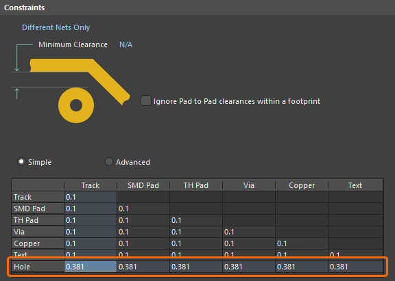
| Hole-to-Object Clearance Checking | Designers can check clearances between the edges of drill holes and neighboring copper objects on signal layers. This is particularly beneficial in preventing the routing of track too near to a drilled hole, which could otherwise suffer from potential wandering of the drill during board fabrication. The row at the bottom of the Clearance rule's minimum clearance matrix is used to define the desired clearances ( |
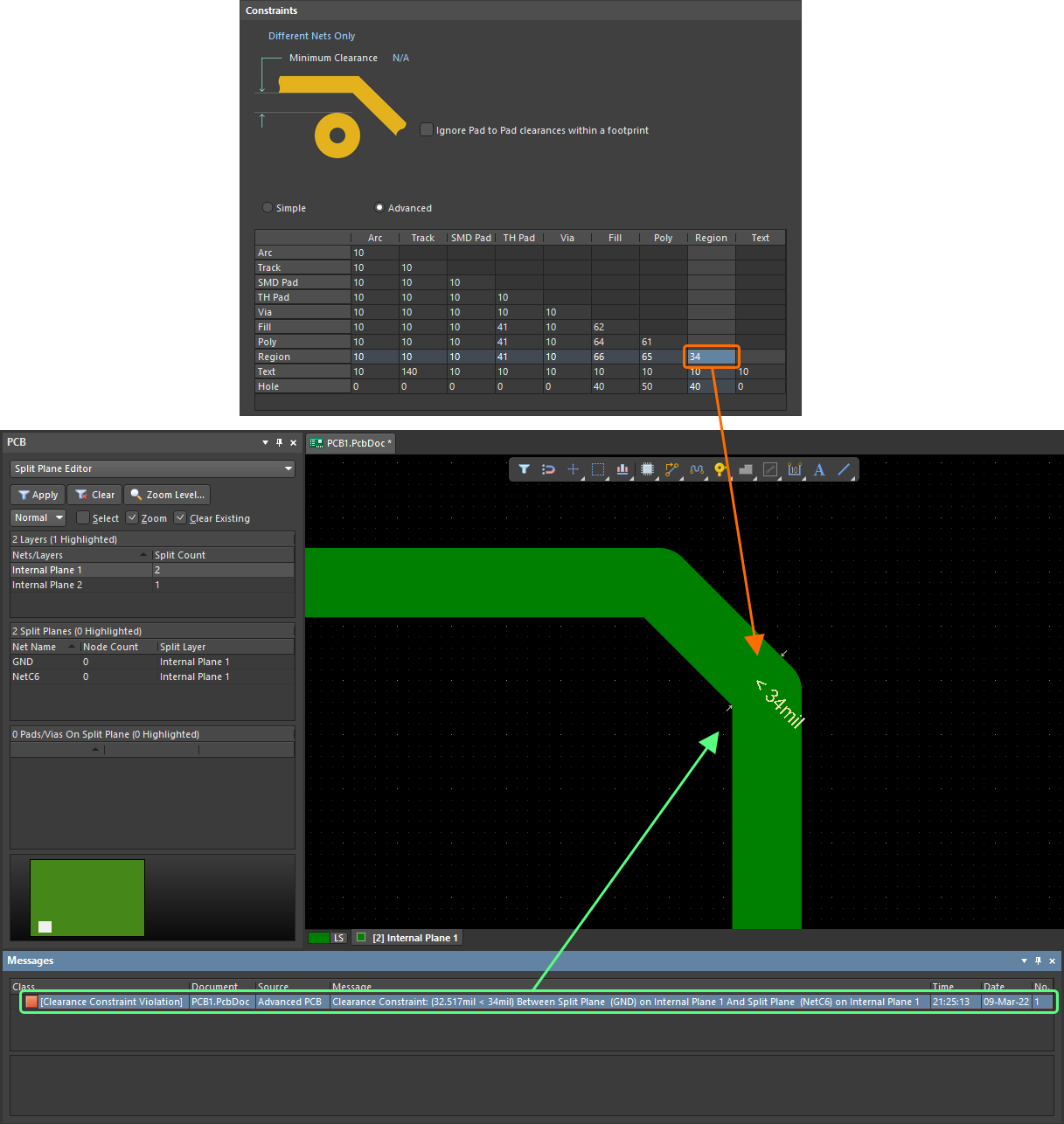
| Split Plane Clearance Checking | This rule can also check clearances between split plane regions on internal plane layers. How clearance is defined depends on the mode in which you are using the minimum clearance matrix:
A violation will appear in the form: Clearance Constraint: (<CurrentClearance> < <DefinedClearance>) Between Split Plane (<NetName>) on <InternalPlaneLayerName> And Split Plane (<NetName>) on <InternalPlaneLayerName>, for example ( Clearance Constraint: (32.36mil < 34mil) Between Split Plane (GND) on Internal Plane 1 And Split Plane (NetC6) on Internal Plane 1 |
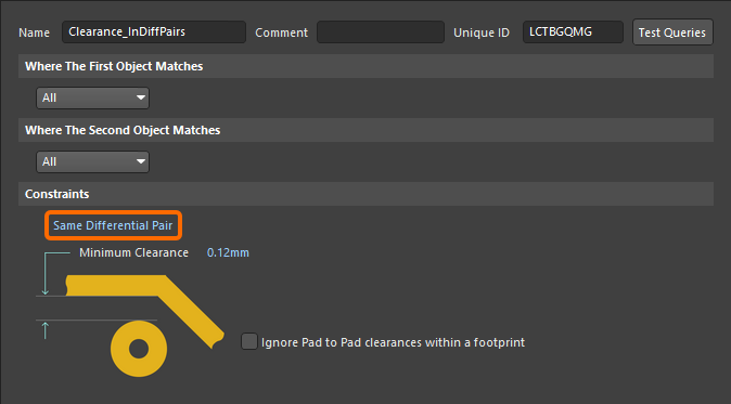
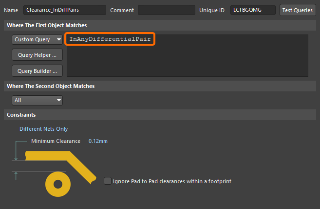
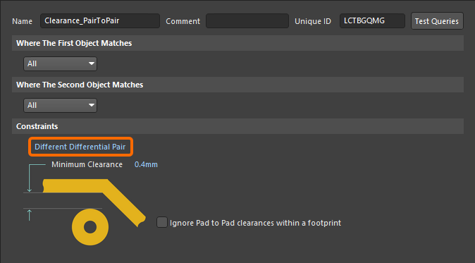
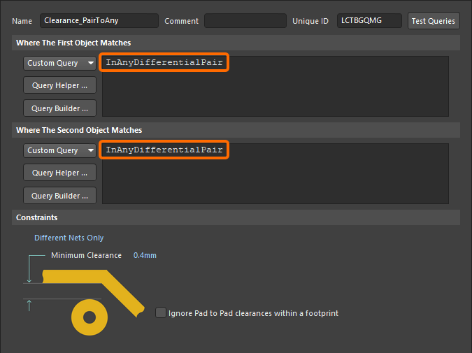
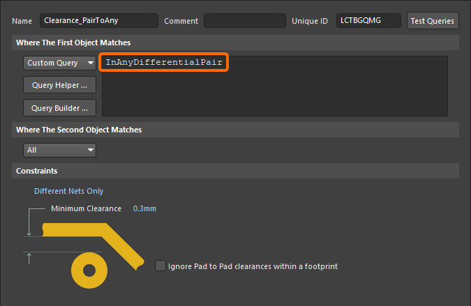
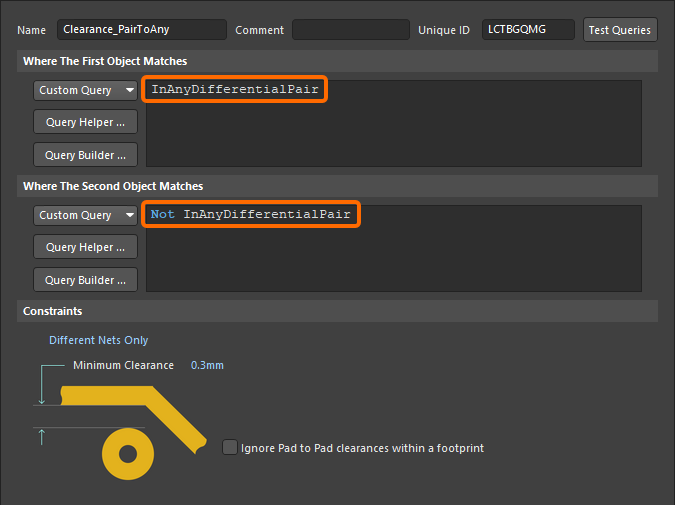
| Differential Pair Clearance Checking | Differential pairs present unique design challenges, often requiring a specific
Learn more about Differential Pair Routing. Learn more about scoping Differential Pair design rules. |
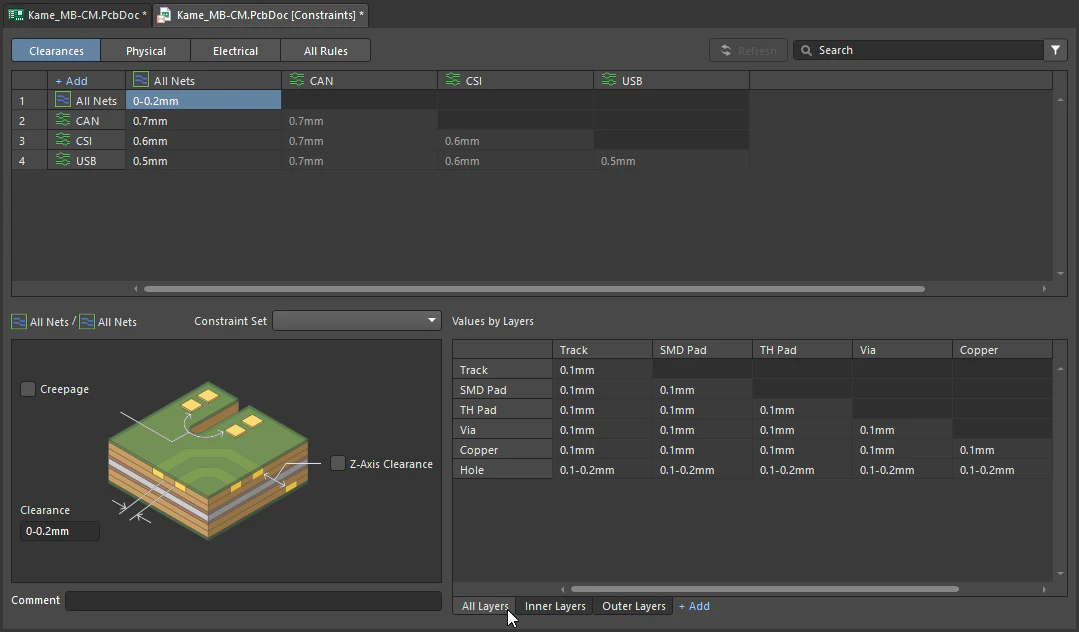
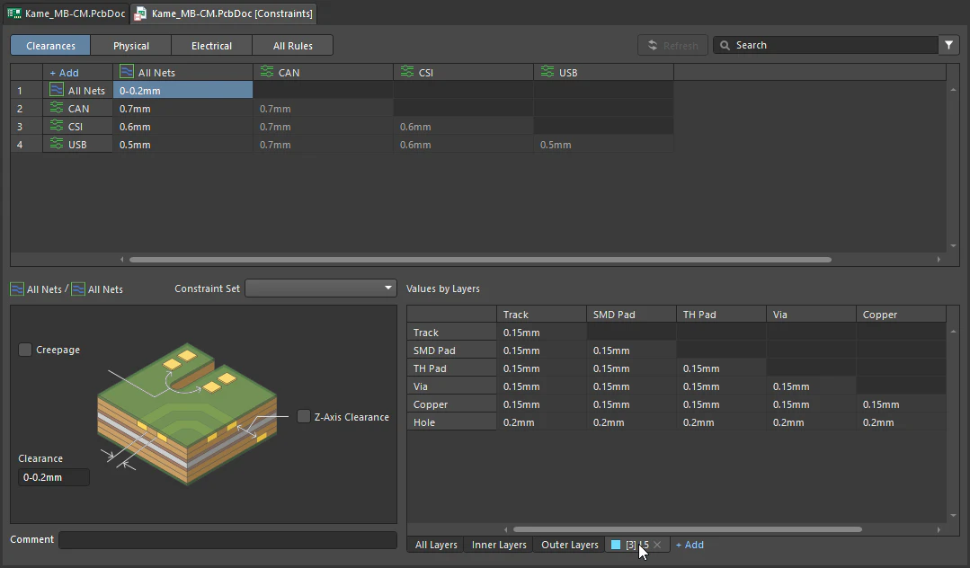
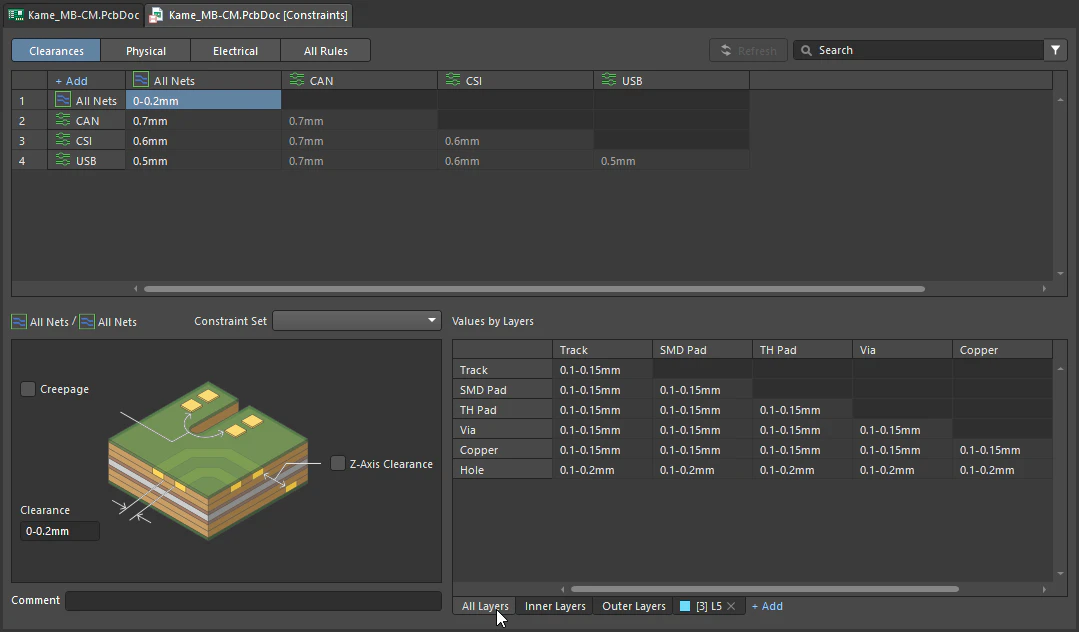
| Clearance by Layer Checking | By default, clearance checking applies to all layers in the design. If the design constraints are defined in the Constraint Manager, the clearance can also be constrained by layer (
|
| Avoid slowing clearance checking | During routing (and similar operations), the rules engine constantly checks for obstacles around the point of editing. The area scanned will include the area of the primitive plus the clearance area required around that primitive. That means the larger the clearance defined in the rules the larger the area that needs to be scanned, and therefore, the slower that the operation will be. If a large clearance is only needed for a small number of objects, you can avoid slowing the routing engine by adding a keepout around these specific objects instead of defining a large clearance rule for them. |
| Clearance checking a printed electronics design |
|
| Rule Application | Online DRC, Batch DRC, interactive routing, autorouting, and polygon placement. |
 )
)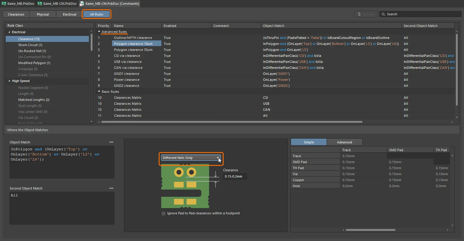 ).
).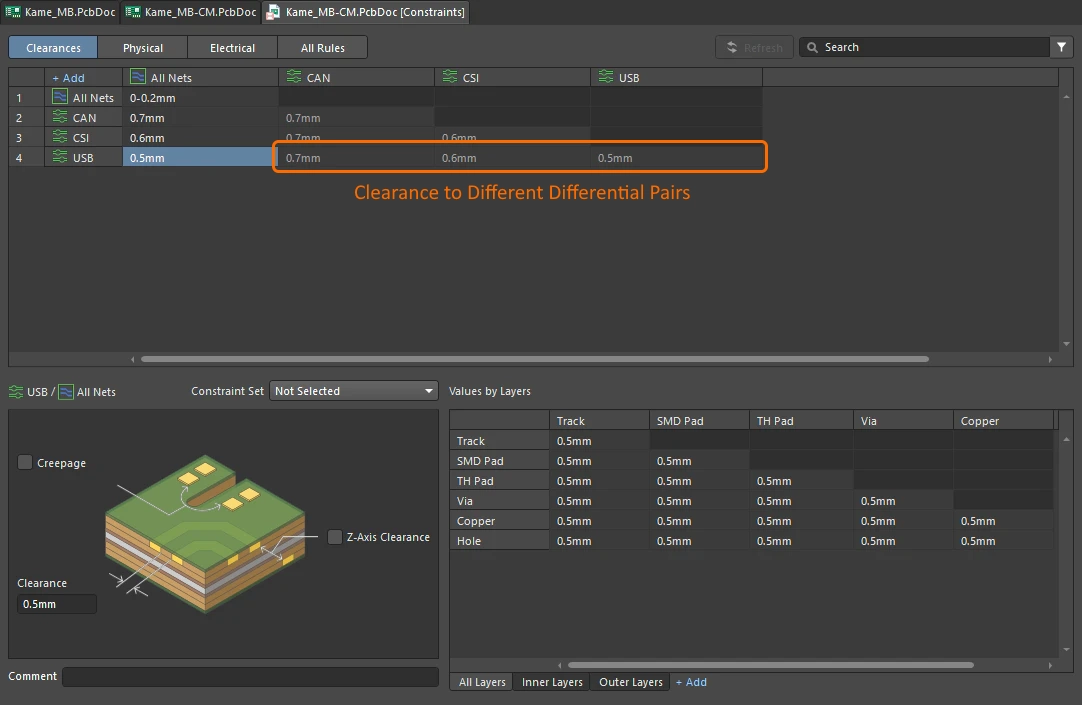 )
)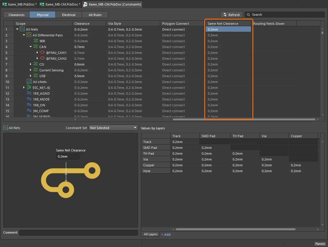 )
)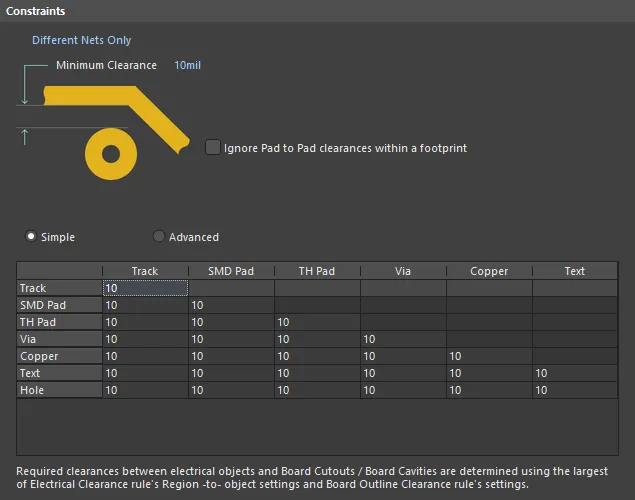 ).
). )
)
 ).
). ).
). )
) ).
). ).
). ).
). ).
). ).
). ).
). ).
). ).
). ).
).Short-Circuit
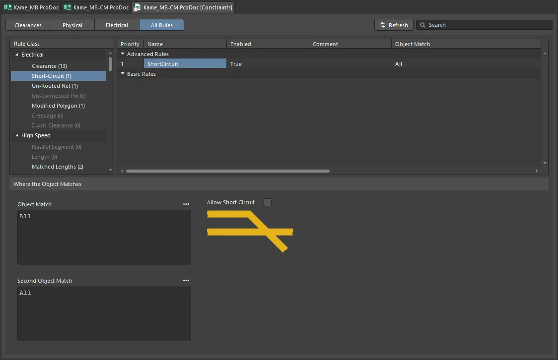
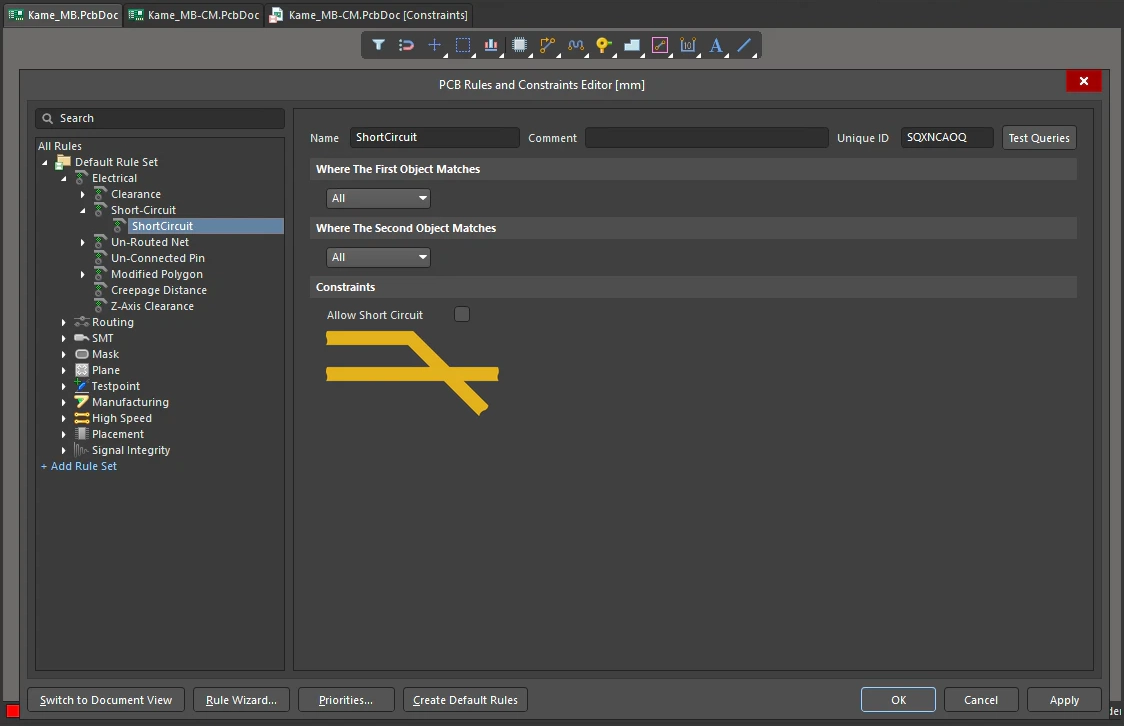
This rule tests for short circuits between primitive objects on the copper (signal and plane) layers. A short circuit exists when two objects that have different net names touch.
Constraints
Short-Circuit Constraint Settings
| Default Rule | Required |
| Allow Short Circuit | Defines whether the target nets falling under the two scopes (full queries) of the rule can be short-circuited or not. If you require two different nets to be shorted together, for example when connecting two ground systems within a design, ensure that this option is enabled. |
| In a printed electronics design | In a Printed Electronics design when different nets cross over on different layers, they are flagged as a short circuit. These cross-overs are isolated by placing a dielectric patch on a non-conductive layer. |
| In a wirebonding design | This rule also applies to Wire Bonding. A violation occurs when a bond wire is connected to a die pad or copper of a different net or when endpoints of bond wires of different nets are connected. |
| Rule Application | Online DRC, Batch DRC, and during autorouting. |
Un-Routed Net
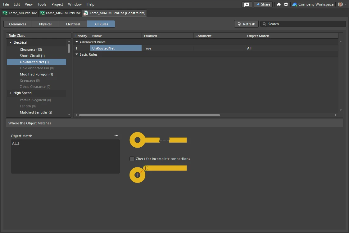
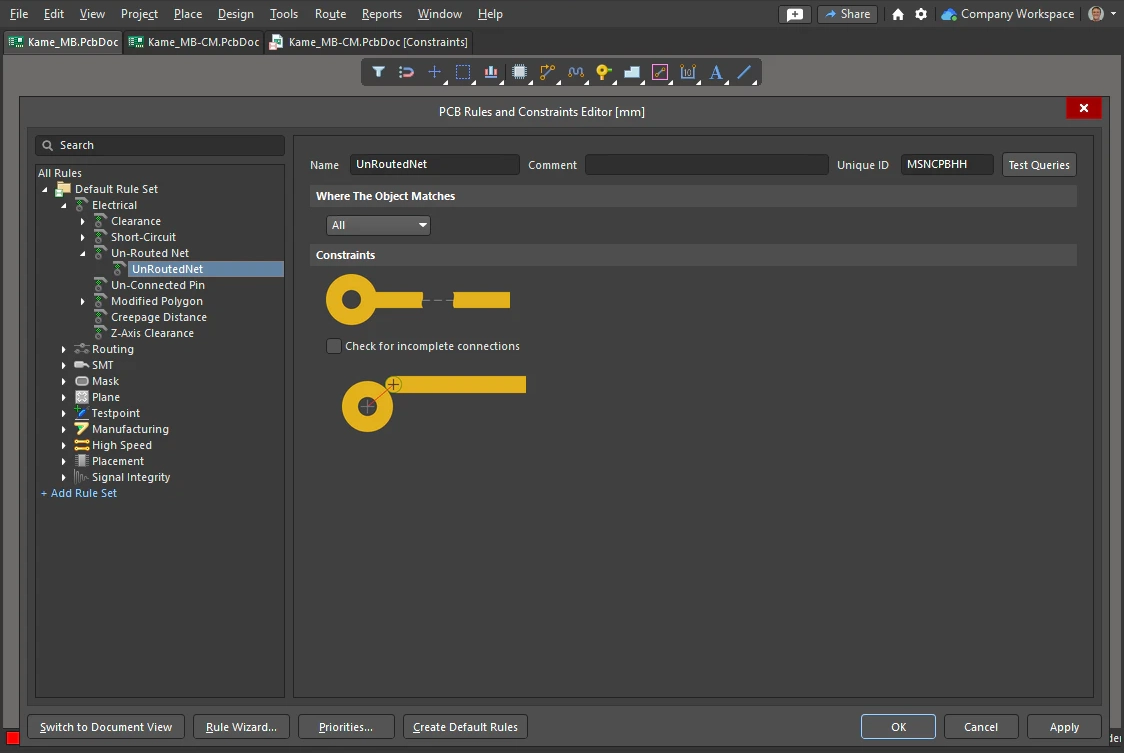
The PCB Editor's Design Rule Checking system typically sees a net as being routed if all nodes in that net (component pads) are connected through the use of net-aware design objects (tracks, arcs, pads, vias, and polygons). These objects are considered connected if they touch each other. However, while simply touching makes a perceived connection to the software, when it comes time to fabricate the board, the fragility of some of these 'connections' can cause critical issues, especially where the objects - for example two contiguous track segments, or a track entering a pad/via - are only slightly touching. Such connections are often referred to as 'Bad Connections', 'Poor Connections', or 'Incomplete Connections'. Use this rule to test for such poor connections.
Constraints
Un-Routed Net Constraint Settings
| Default Rule | Required |
| Routing completion | This rule tests the completion status of each net that falls under the scope (full query) of the rule. If a net is incomplete then each completed section (sub-net) is listed along with the routing completion. The routing completion is defined as:
|
| Check for incomplete connections | With this option enabled, the following additional checks on connectivity between applicable design objects are made:
|
| How failures are identified |
|
| Interaction with other rules | Some DRC checks require the Un-Routed Net rule to be Batch-enabled for them to work. |
| In a printed electronics design | In Printed Electronics, layer transitions do not require a via, the net analyzer will recognize that the net is not broken if a via is removed from a routed net. A board is defined as Printed Electronics when the Printed Electronics option is enabled in the Layer Stack Manager. Learn more about Printed Electronics. |
| In a wirebonding design | This rule also applies to Wire Bonding. A violation occurs when there is no connection between die pads, bond wires and/or copper objects of the same net. |
| Rule Application | Batch DRC. |
 , with a corresponding message appearing in the Messages panel.
Un-Connected Pin
This rule detects pins that have no net assigned and no connecting tracks.
Constraints
Un-Connected Pin Constraint Settings
| Default Rule | Not required |
| Settings | None |
| Rule Application | Online DRC and Batch DRC. |
Modified Polygon
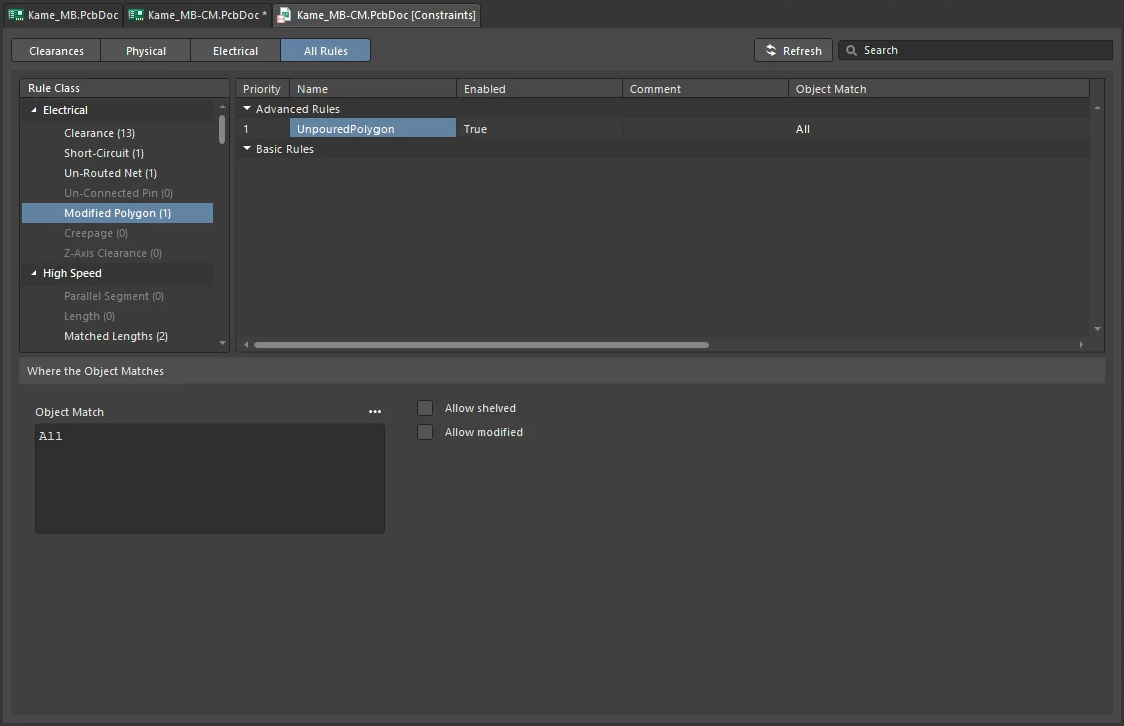
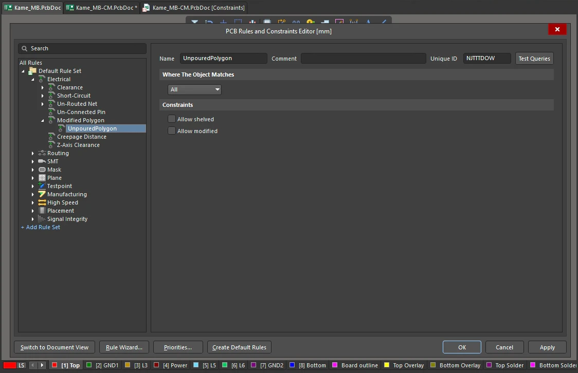
This rule detects polygons that are still shelved and/or have been modified but have not yet been repoured.
Constraints
Modified Polygon Constraint Settings
| Default Rule | Required |
| Allow shelved | If enabled, all polygons that fall within the scope of this design rule, and that are currently shelved, will not be flagged as a violation. |
| Allow modified | If enabled, all polygons that fall within the scope of this design rule, and that are currently modified but have not been repoured, will not be flagged as a violation. |
| Rule Application | Online DRC and Batch DRC. |
Creepage Distance
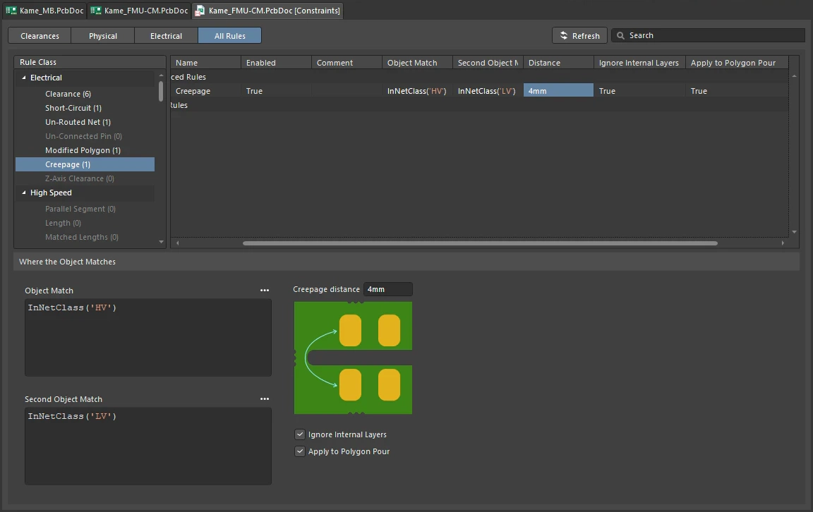
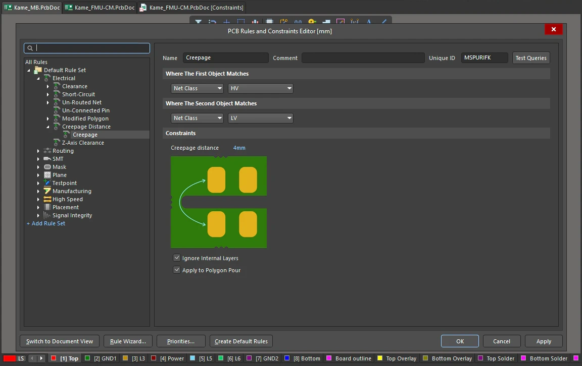
This rule tests the creepage distance between the targeted signals across the board surface through unplated holes, cutouts, and around the board edge.
Constraints
Creepage Distance Constraint Settings
| Default Rule | Not required. |
| Creepage distance | A rule violation is flagged when any point on the First Object is equal to or less than the distance from any point on the Second Object. |
| Ignore Internal Layers | Use this option to ensure the rule will only be applied to outer layers. |
| Apply to Polygon Pour | Use this option to apply the rule to scoped polygons. |
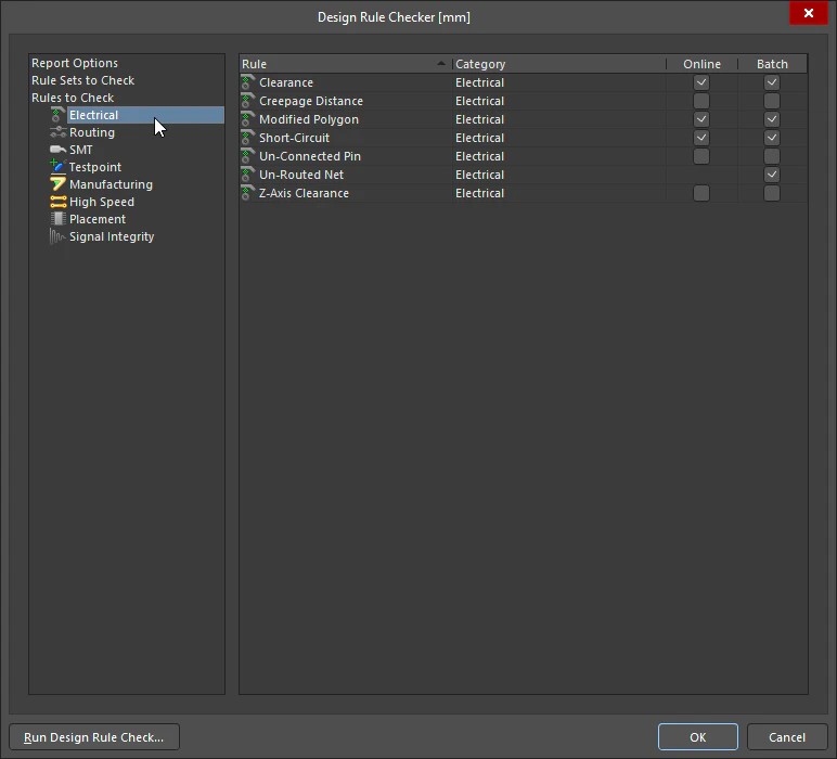
| Default behavior | The Creepage Distance rule is not enabled for Online or Batch design rule checking by default. Enable Online/Batch checking in the Design Rule Checker dialog ( |
| Results | The rule identifies the closest points on the targeted nets and checks the distance between them in the X, Y, and Z planes. |
| Slotted pad | If a board slot has been created by placing a pad, make sure that the Plated option is disabled in the pad properties as the software assumes that the plated barrel is conductive and will reduce the creepage distance accordingly. |
| Polygon behavior | If a polygon pour and other objects are scoped by a Creepage Distance design rule with the Apply to Polygon Pour option enabled and a Clearance design rule, both rules are considered, and a larger value is applied when pouring the polygon. For example, if the Creepage Distance rule has a larger constraint value than the Clearance rule, this larger value will be applied. |
| Rule Application | Online DRC, Batch DRC, and during autorouting. |
 ).
). ).
).Z-Axis Clearance
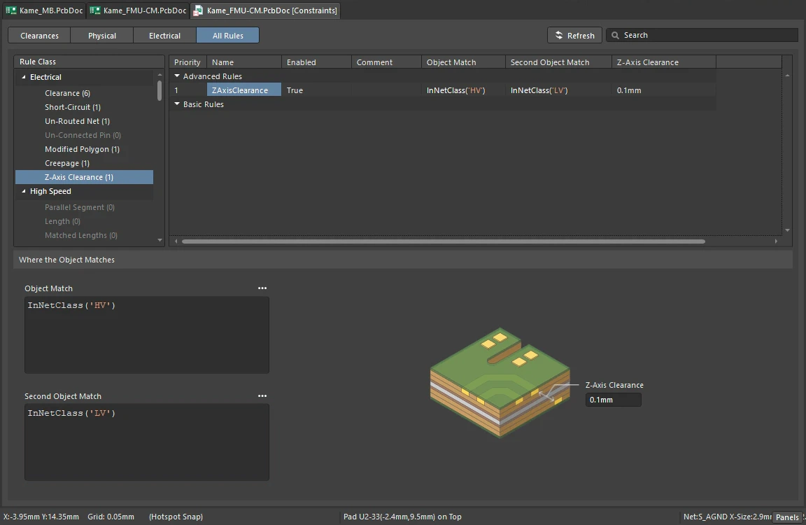
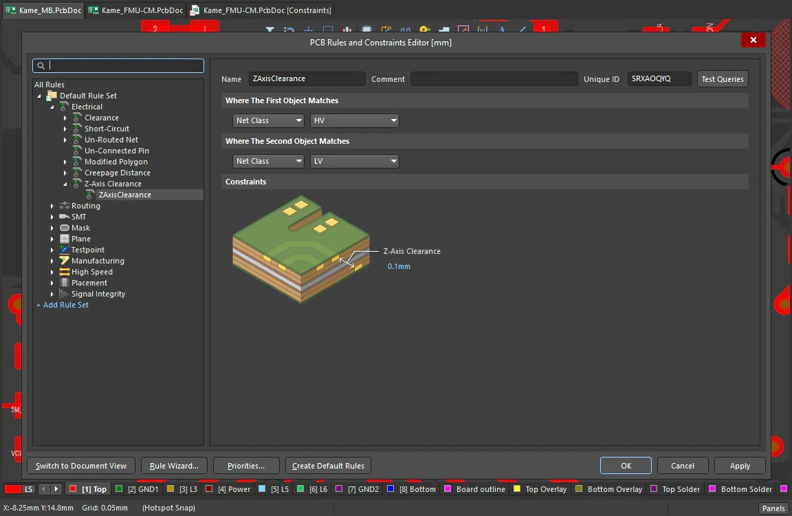
This rule tests the minimum clearances between various primitives on different copper layers.
Constraints
Z-Axis Clearance Constraint Settings
| Default Rule | Not required. |
| Z-Axis Clearance | A rule violation is flagged when any point on the first object is equal to or less than the distance from any point on the second object when the first and second objects are placed on different copper layers. |
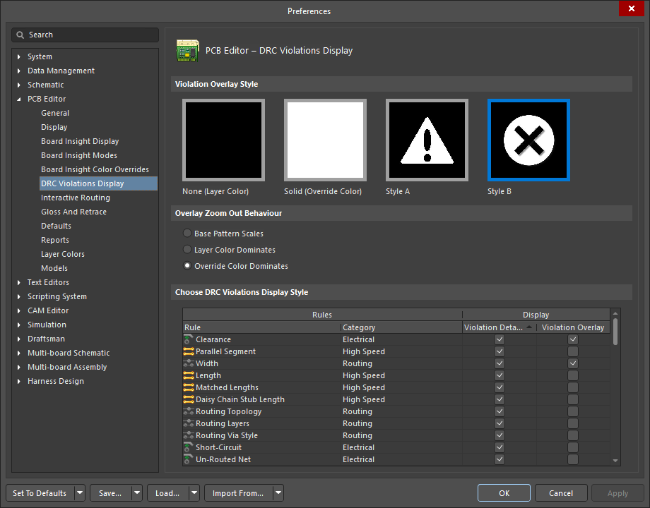
| Display of violations | With display of Violation Details enabled for the PCB Editor – DRC Violations Display page of the Preferences dialog (
where the In other places within the software, the following format is used:
|
| Support for polygons | The rule is supported by polygon pours (solid and hatched) and internal planes. Note that voids are made for polygons only when a violation is detected between a polygon and objects of other types (tracks, pads, etc.). While clearances and violations are detected between polygon pours on different signal layers, voids are not created automatically in this case. |
| Support for plane layers | While clearances and violations are detected between objects (placed on signal layers) and internal planes (by the shortest distance), such violations must be resolved manually. |
| Saving in an older file format | When opening a PCB containing defined Z-Axis Clearance rules/constraints in an older version of Altium Designer that does not support this feature, the rules will be lost. |
| Rule Application | Online DRC, Batch DRC. |