
Improvements in Beta
This page includes detailed information for features and functionality that are currently available to Beta users.
Version 26.10
Altium Designer Develop – Released: 26 August 2026 – Version 26.10.0 (build 5)
Altium Designer Agile – Released: 26 August 2026 – Version 26.10.0 (build 24)
Altium Designer – Released: 26 August 2026 – Version 26.10.0 (build 4)
Beta Release Notes for Altium Designer
PCB Design Improvement
Design Rule Sets (Open Beta)
This release introduces the concept of Rule Sets to the PCB Rules and Constraints Editor dialog, allowing for the efficient grouping and reuse of a set of design rules specific to, for example, an interface or manufacturer. You can quickly:
-
Create a new rule set or duplicate an existing set (and then modify further as required).
-
View and manage the constituent rules within a set, with the ability to move a rule between sets.
-
Switch between applied sets of rules – enabling/disabling sets as desired.
-
Rename or delete a rule set.
-
Export/import rule sets for optimal portability. When importing, you can choose to import rules in a set to an existing rule set or to a newly-created one. In addition, import allows you to choose whether, for a same-named rule set, the rules in the imported set should be merged (added) into the existing set (and adding a suffix to any same-named rules), whether all selected rules should be added (and, in case of a conflict, an existing design rule will be replaced with the rule from the file), or whether the rules in the existing set should be removed and replaced fully by those in the imported set.
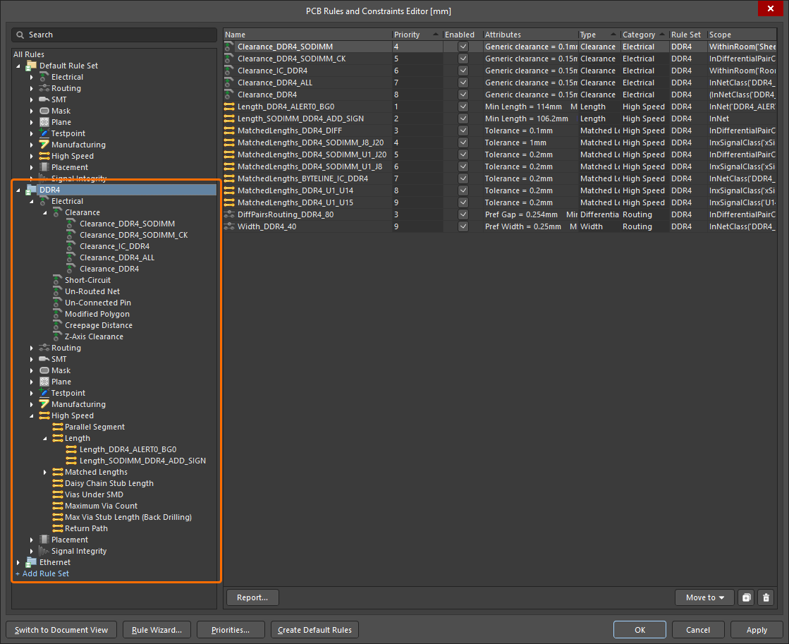
DDR4 and Ethernet rules sets have been defined to group design rules related to the corresponding interfaces.
The priority system works as before. In each rule set, only one rule of a given type (with the highest priority) is evaluated. Design rules of each type have a 'global' priority list across all rule sets, meaning that if an object in the PCB document is covered by more than one rule, the highest priority rule will apply, irrespective of the rule set to which it belongs.
In addition, the Design Rule Checker dialog includes a new Rule Sets to Check page, from where you can configure force batch checking for rule sets (provided more than one rule set exists). When the Force Batch Check option is enabled for a rule set, not only an applicable rule of the highest priority for each rule type will be checked, but also an applicable rule of the highest priority for each rule type, within this rule set, will be force-checked during Batch DRC. Essentially, force-checking runs in parallel to normal batch DRC, executing an additional DRC run for each rule set included for force checking (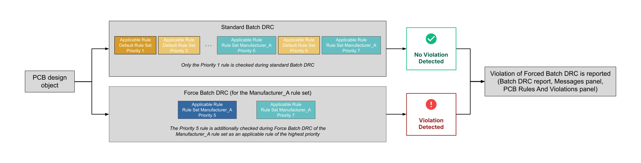 ).
).
The PCB Rules And Violations panel and Messages panel, as well as the Design Rule Verification Report, have also been updated to include rule set information.
For example, if a net is scoped by a Width rule in the Default Rule Set and a Width rule in a user-created rule set, this net will be additionally checked against the Width rule from the user-created rule set if the Force Batch Check option is enabled for this rule set, even if this rule has a lower priority than the Width rule from the Default Rule Set. Entries for detected violations of design rules that are included in force-checked rule sets are labeled Force Checked <RuleSetName> in the DRC report, the Messages panel, and the PCB Rules And Violations panel.
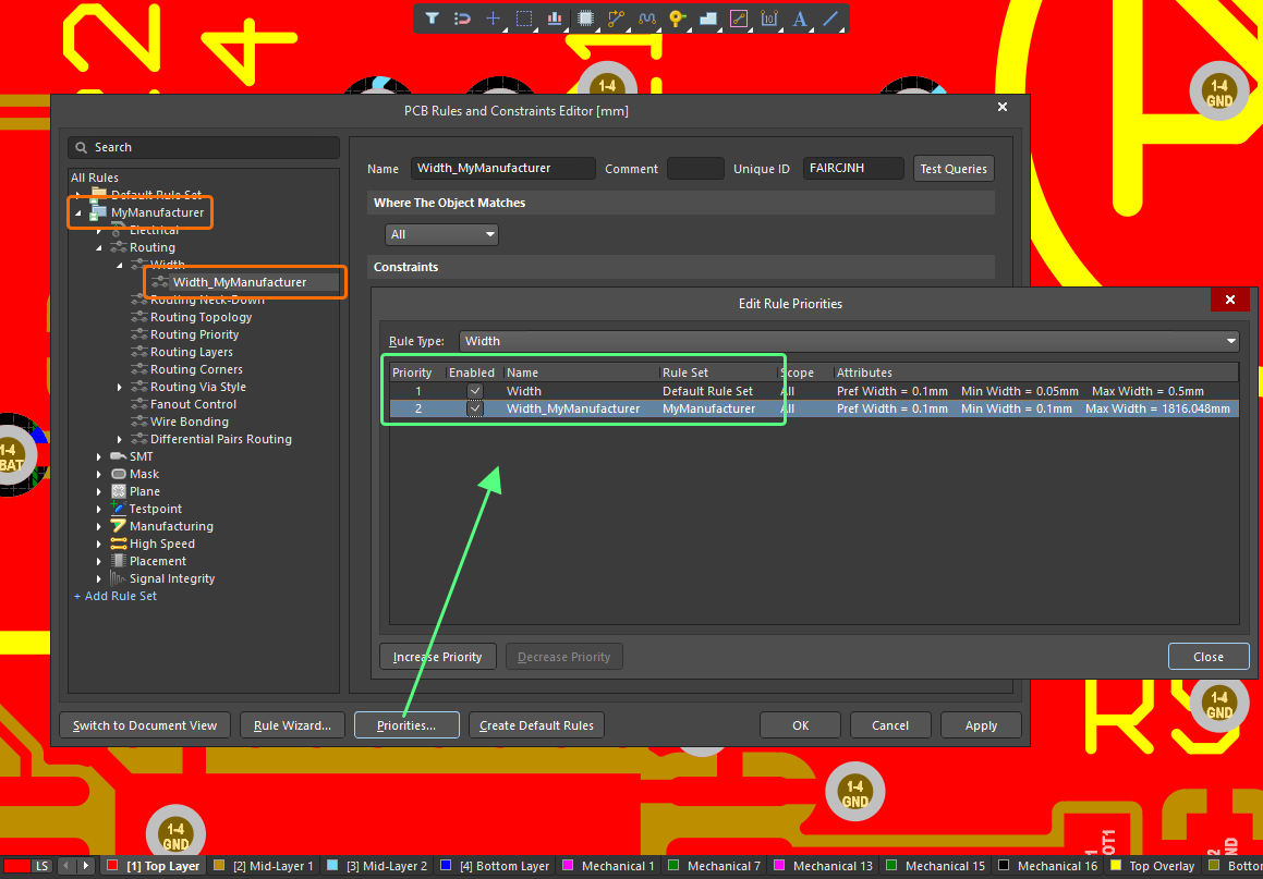
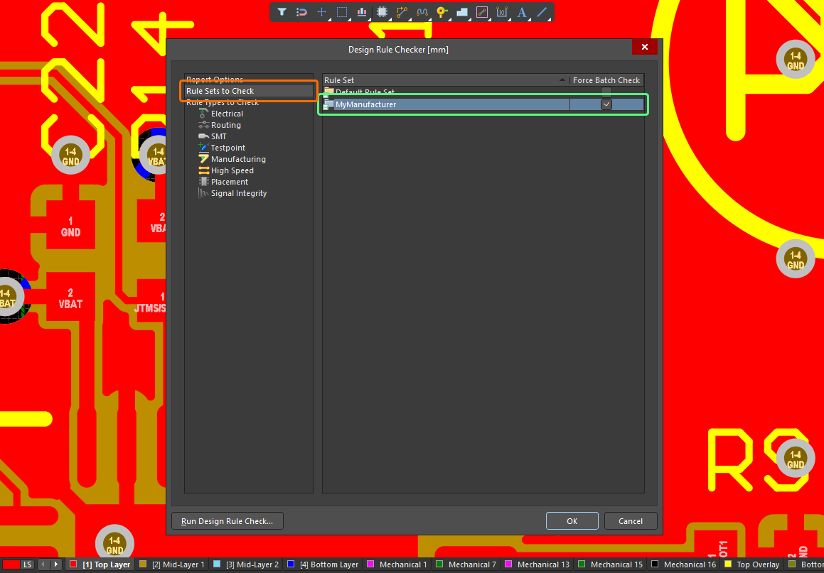
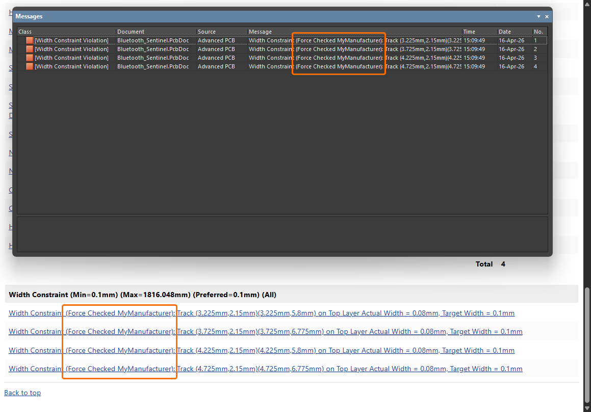
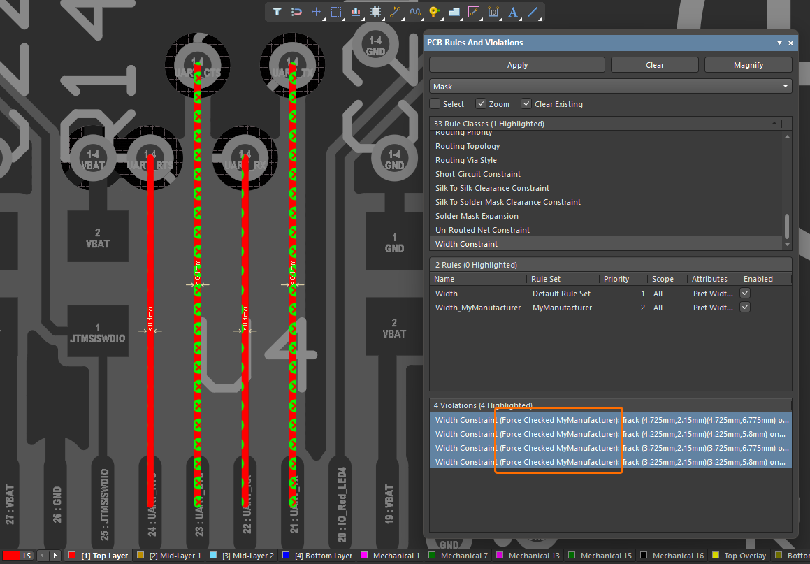
For more information, refer to Defining, Scoping & Managing PCB Design Rules and Setting Up & Running a DRC pages.
Harness Design Improvements
Layout Label Follows Bundle Orientation
Layout labels now automatically observe the orientation of the harness bundle to which they are attached. The layout label 'snaps' to the bundle in order to mimic the orientation and path. During or after placement of the layout label, you can press the Spacebar to rotate the label in increments of 90 degrees at a time or update the Rotation value in the Properties panel.
If you do not want the label to follow the orientation of the bundle (i.e. not 'snapped'), press the Alt key during placement to place the label in the required location, as shown in the video below.
When the bundle that includes a 'snapped' label is moved, the layout label position is recalculated and follows the bundle.
For more information, refer to the Creating the Layout Drawing page.
Ability to Independently Adjust Width/Height of Some Harness Objects
You can now adjust the width and height of a cable, shield or twist object that is placed in a harness wiring diagram (*.WirDoc). A new lock control associated with the Width/Height fields in the Properties region of the Properties panel (with an object selected) allows you to switch between locked or unlocked dimensions. When the object is dragged by its editing handles, the aspect ratio is followed according to the setting. The default is locked, which gives a height:width aspect ratio of 2:1 (for a cable or shield) or 1:1 (for a twist). When unlocked, you can independently change the dimensions as required.
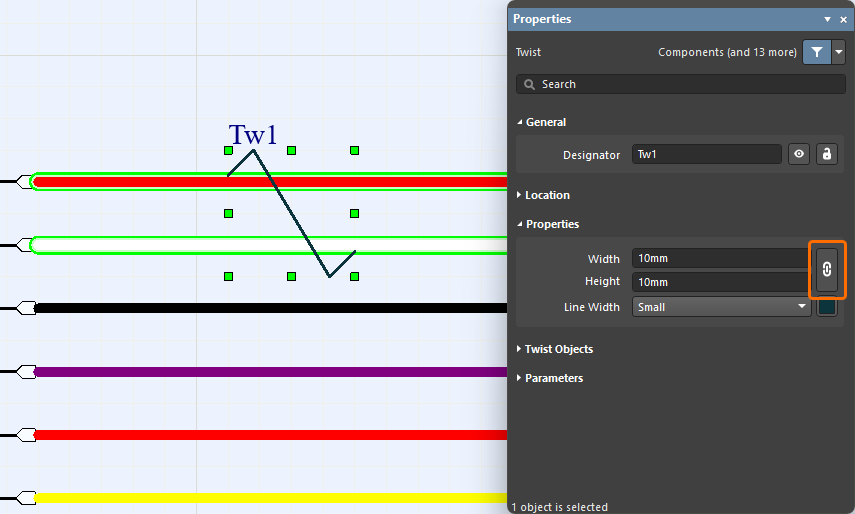
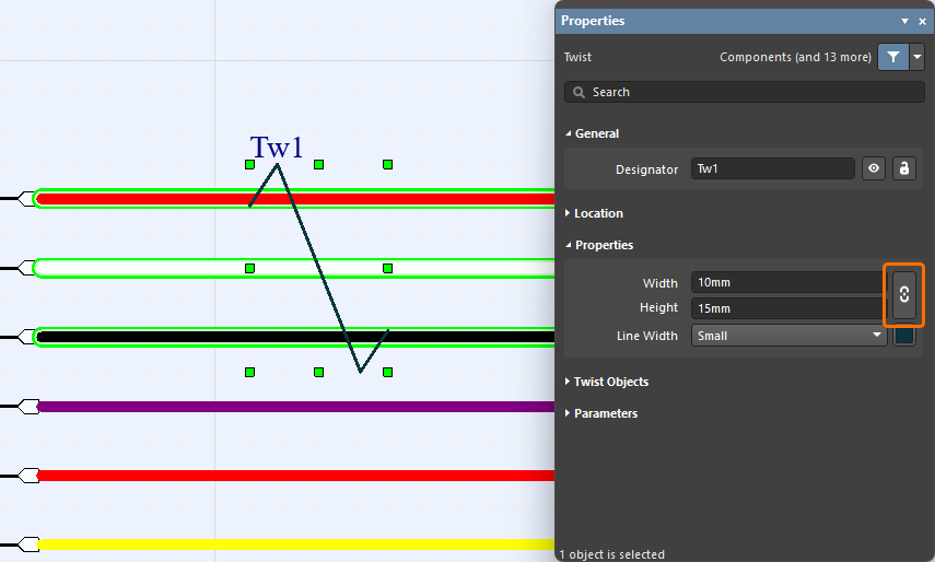
For more information, refer to the Defining the Wiring Diagram page.
Data Management Improvements
Defining Component Name and Description Using Parameters
It is now possible to use parameters to define the Name and/or Description when creating a new component (or editing an existing released component) in the connected Workspace (e.g., [ParameterName1]_[ParameterName2]), provided the parameters (with values) have been defined for the component. This feature is supported in both Single Component Editing and Batch Component Editing modes of the Component editor.
In the example shown below, the Name field of a capacitor component is defined based on its Value, Tolerance, Voltage Rating, and Case/Package parameters.
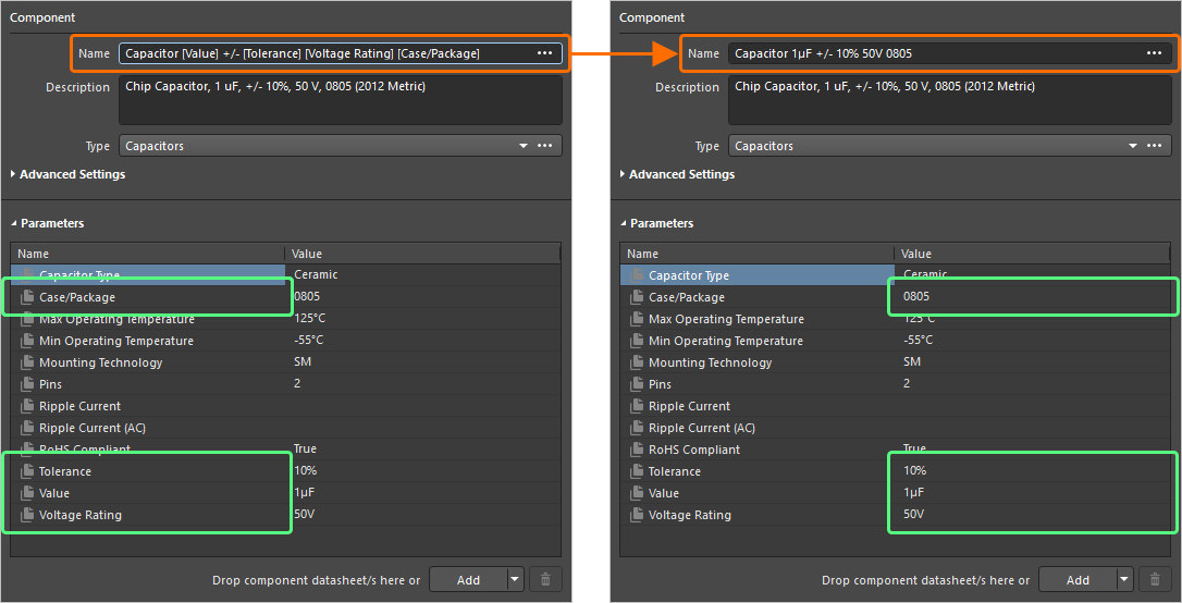
For more information, refer to the Single Component Editing and Batch Component Editing pages.
Enhancements to Custom Parts Provider Synchronization
The Custom Parts Provider Synchronization feature has been enhanced to include additional Category and Datasheet system parameters, as well as support for custom parameters, in an underlying Custom Parts Provider Synchronization Configuration document (*.PrtSync).
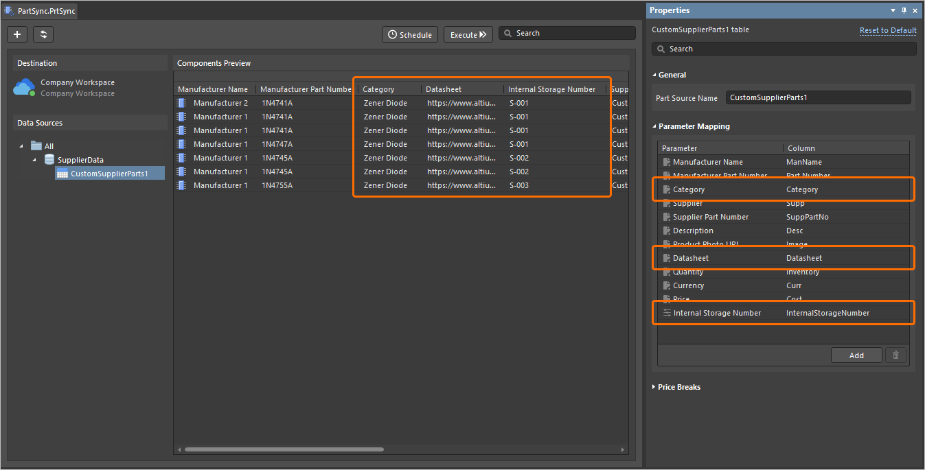
Support for these parameters has also been added to the Manufacturer Part Search panel. This requires the EDMS.CustomOffersMerge option to be enabled in the Advanced Settings dialog, which merges supplier data from your configured Custom Parts Provider with the Altium Parts Provider, to present all supplier information combined (Note: This 'Supplier Data Merging' feature is only available when connected to a Workspace on the Altium Platform that has BOM Portal enabled).
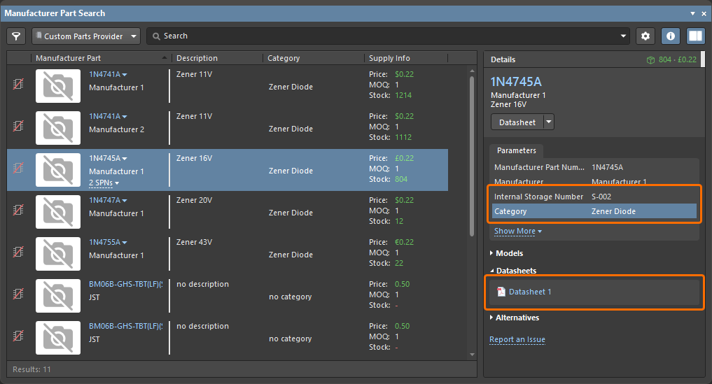
For more information, refer to the Supply Chain Database to Workspace Data Synchronization page.
Improved Name Field Search Functionality
When using the Component editor in Single Component Editing mode, the Name field has been enhanced with respect to its search functionality. Searching will now only begin after entering at least two characters, with hint text to highlight this.
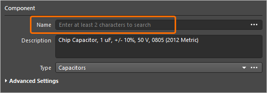
For more information, refer to the Single Component Editing page.
Feature Made Fully Public in Altium Designer 26.10
The following feature is now officially Public with this release:
Additional Features in Altium Designer 26.10
-
Dedicated Layer Assignment for IPC Compliant Footprint Wizard: A new advanced settings option –
PCB.IPCWizard.DedicatedLayerAssignment– is available in the Advanced Settings dialog with this release that, when enabled, assigns dedicated layers for component center and designator primitives, and also automatically creates Assembly/Courtyard layer pairs. Note: Keep this option disabled to prevent compatibility issues with existing libraries and templates that were created prior to Altium Designer 26.7. -
Open CASCADE 7.9.0 (Open Beta): A new advanced settings option –
PCB.UseOpenCascade790– is available in the Advanced Settings dialog with this release which, when enabled, switches to use version 7.9.0 of the Open CASCADE library for processing of 3D geometry in Altium Designer.
Features in Closed Beta
Key Features Entering Closed Beta in Altium Designer 26.10
The following key features have entered Closed Beta for the first time in this release:
Existing Closed Beta Features Improved in Altium Designer 26.10
The following existing Closed Beta features have been improved further in this release:
Advanced Via Fencing
This release delivers advanced support when using via fencing (adding shielding and stitching vias) in a PCB design and is especially relevant to RF and High-Speed designs which, due to their inherent complexity, require a stronger, more accommodating and robust, via fencing tool.
Enhanced shielding and stitching support is delivered through the Properties panel, which presents controls for Via Fencing in ’Shielding’ or ‘Stitching’ modes, depending on the selected existing fencing entity in the PCB design space (or chosen entity if adding new fencing for the first time).
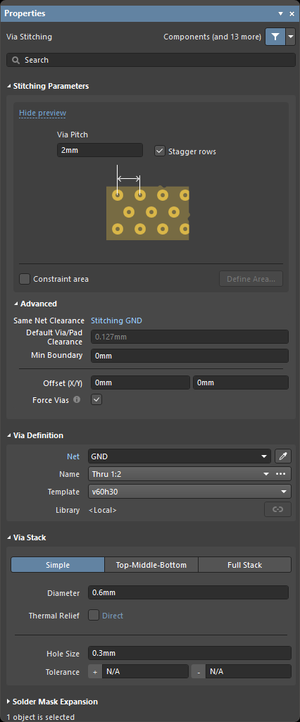
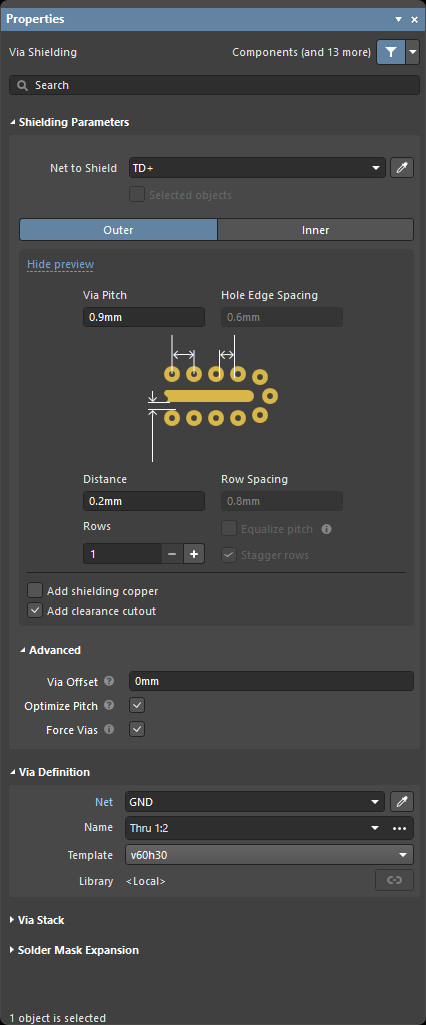
The panel provides all the controls needed to configure fencing exactly as you need it:
-
Apply different shielding via patterns to the same net on different layers. This caters for the common case of adding different via patterns on traces on layers between signal transition vias.
-
Place stacked vias into the shielding.
-
Shield with staggered vias using a new, configurable ‘via offset’.
-
Fence by geometry edge (polygonal-shaped objects or the board outline) in a selected area. Expanding on the previous ability to follow the ‘outer’ side of the selected geometry, you can now set up to follow the 'inner' side as well. This enables you to surround different RF-sensitive areas, such as Faraday cage, Coplanar Waveguides, RF walls perimeter (to limit the fringing fields along the board outline), etc.
-
Fencing obeys Clearance, Short Circuit, Hole to Hole, and Board Outline Clearance design rules.
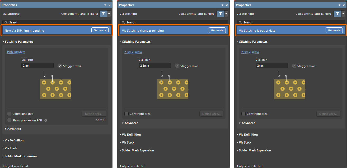
The Properties panel also guides you through the various states that can be encountered, with relevant messaging and action controls for:
-
Generating an initial via shielding/stitching pattern. If there is existing shielding for a net, you will have the choice to add the newly defined shielding or replace the existing shielding completely.
-
Pending changes, where modifications to an existing shielding/stitching pattern have been made in the panel and have yet to be applied to the design itself.
-
Board changes, where objects/geometry within the design have changed and the associated shielding/stitching has become ‘out of date’.
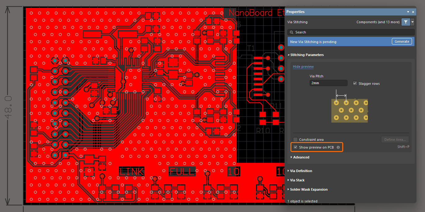
You also have the convenience of seeing a preview of the shielding/stitching pattern, prior to its generation, though be aware that the final pattern generated in the design may change slightly to accommodate DRC.
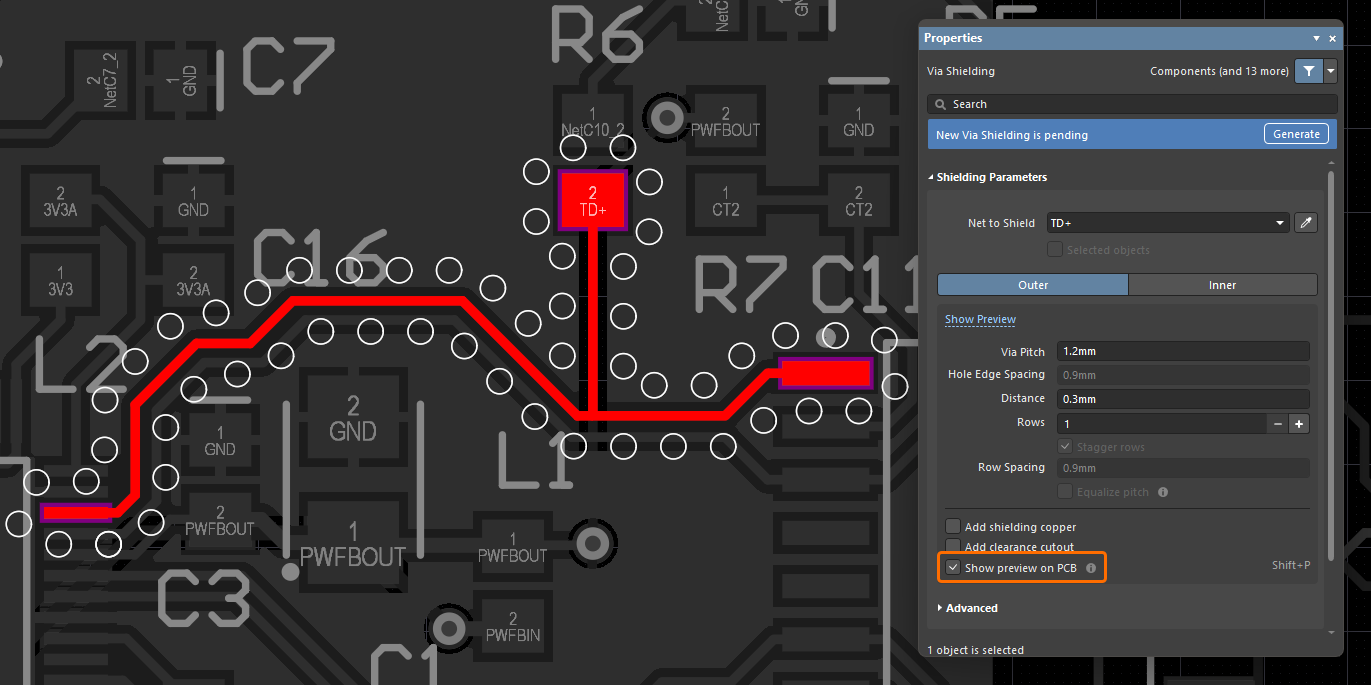
Whether generating a new shielding/stitching pattern or updating an existing one, a dialog will present the results of how many shielding/stitching vias were generated or omitted (in adherence to defined design rules). If no vias were generated, you can either interrogate and modify applicable rules or use a Force vias control, available in the Properties panel (which places vias that will violate those design rules).
For more information, refer to the Adding Via Stitching & Via Shielding page.
Modern Comment Markers
In this release, a new design has been introduced for comment markers placed in the design space. The new markers are available wherever comments are supported. This feature also includes new coloring when placing comments in an ActiveBOM document.
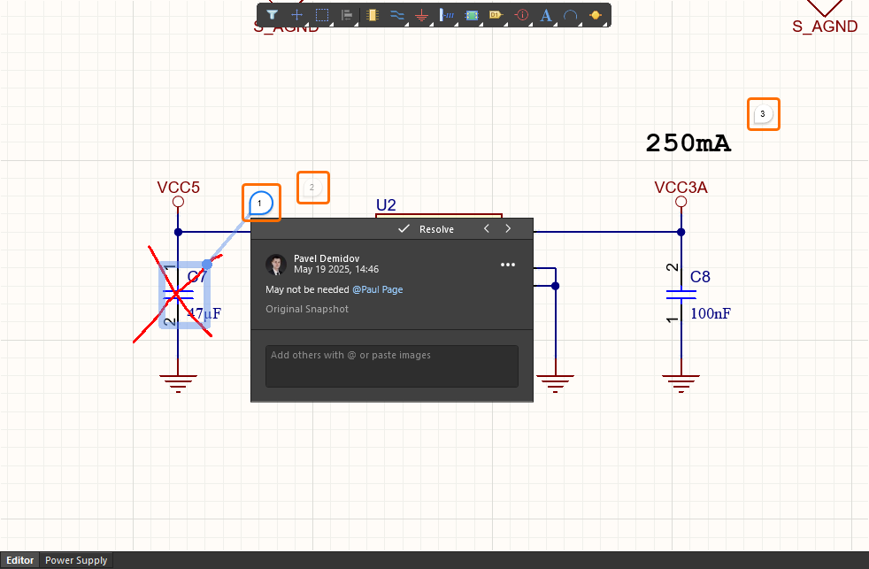
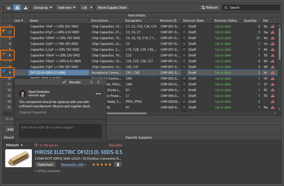
For more information about the commenting functionality, refer to the Document Commenting page.
Advanced Diff Pair Retrace
This release adds enhanced support for retracing a selected differential pair when the Hugging Style is set to Rounded mode in the Gloss And Retrace panel. The Set Diff Pair Gap field is now provided in the Retrace Parameters region of the panel that allows you to select one of the rule-based gap options (Min / Max / Preferred) of an applicable Differential Pairs Routing design constraint when the Retrace Selected command is run, or retrace using the Current gap between the differential pair tracks. Alternatively, enter a desired custom gap value directly in the field.
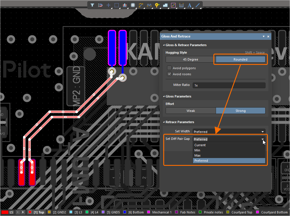
For more information, refer to the Interactive Routing page.
Harness Library Components
This release brings support for a range of harness-related component types that can be defined as part of your Workspace Library. At the heart of this support is a new model type that can be created and defined – the Harness Entity. When creating a new component, choosing the Harness Entity model type will take you through to creating one of the following supported models:
-
Harness Connector – a physical, pluggable termination point for bundled wires, providing interconnection to/between electronics modules/circuits in an overall harness loom. Configure its gender, crimp gender and sealing type and whether it has built-in crimping. A ‘cavity view’ of the connector can also be defined (see below).
-
Crimp – a metal terminal where the contact barrel is compressed around the stripped electrical wire. Configure its gender and finish, along with associated, industry-standard parameters.
-
Seal – an environmental barrier around a crimped wire to prevent moisture, dust and debris from entering a connector cavity. Configure the min/max outer diameter (OD). A seal can have an associated plug (a cavity plug or dummy plug), which is used to seal an unused/empty cavity in a sealed connector. So when a sealed connector has a cavity where no wire/crimp is inserted, a plug fills that cavity to ensure the environmental sealing integrity of the whole connector is maintained.
-
Accessory – a physical component used in the routing and organization of harnesses, such as a peg, band, corner post or tie-wrap.
-
Splice – a crimped and insulated mechanical joint used to extend, fork or connect circuits in a harness loom. Configure its type: Butt, Parallel, Reducer, Tap or IDC, along with associated, industry-standard parameters. Note that this is only for mechanical splices.
-
Covering – a length of protective sleeving over a harness bundle to physically protect the bundle against heat and abrasion, for example. Configure its type: Tubing (Standard, Slit or Shrinkable), Corrugated Tubing (Standard or Slit), Spiral Wrap, Tape or Braiding, along with coloring and associated, industry-standard parameters. Note that defining a harness covering is currently supported at the Workspace Library level only.
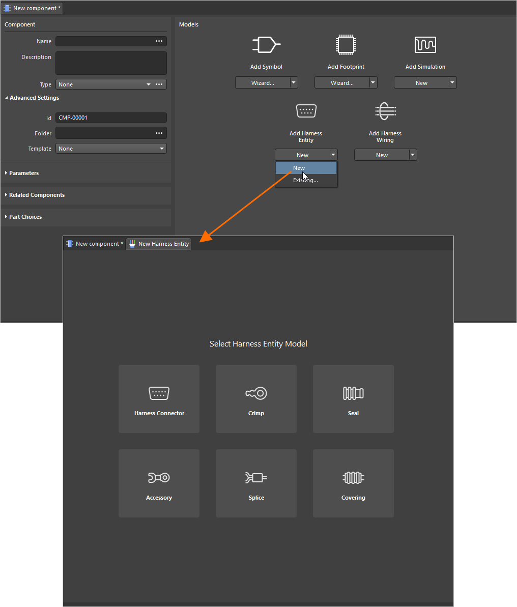
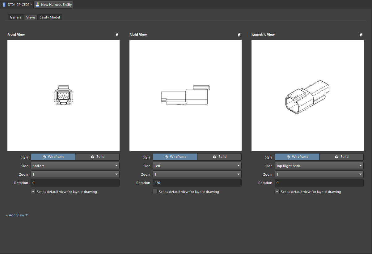
For all but the Covering entity type, you upload a 3D model, which is used as the basis for defining a range of physical model views (projections) for use when placed in the layout drawing. For each defined view, you can configure whether it is solid or wireframe, its projection side, zoom level, and rotation, and whether it is added as default when placing the physical view of the model on the layout drawing.
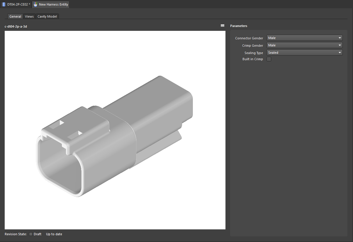
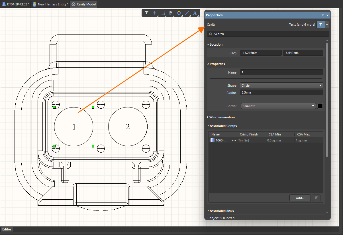
In addition, for a Harness Connector model entity, you can use the uploaded 3D model as a backdrop in the definition of a Cavity Model, which is essentially a graphical view of the connector – a Cavity View, if you will – with its numbered cavities and associated crimps and seals. The model is defined through a new Cavity Model (or Cavity View) editor, with the Properties panel reflecting options and controls at both the model level (with no cavity selected) and the selected cavity level.
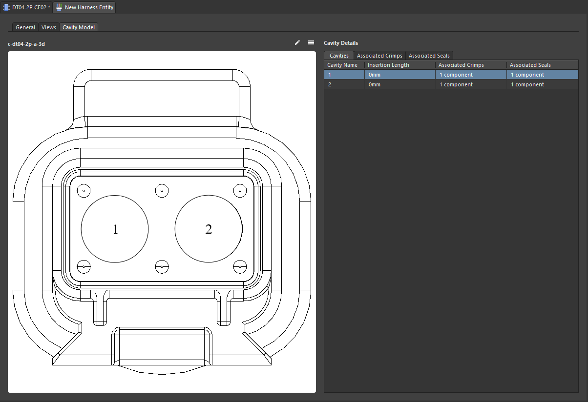
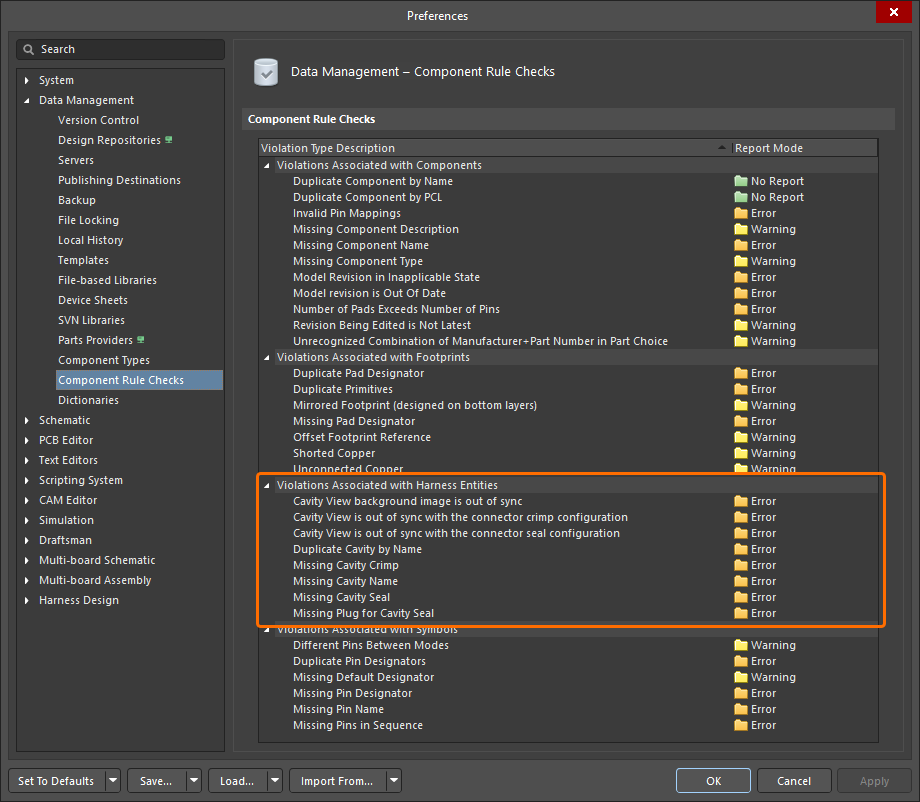
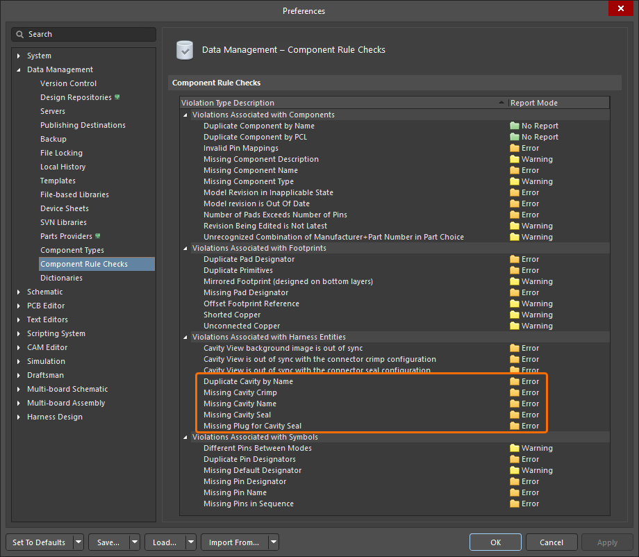
Various new component rule checks have been added with respect to saving a new harness component involving a defined connector model and its cavity model/view, which you can find on the Data Management - Component Rule Checks page of the Preferences, under the new section Violations Associated with Harness Entities.
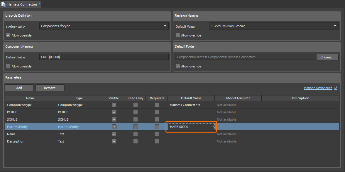
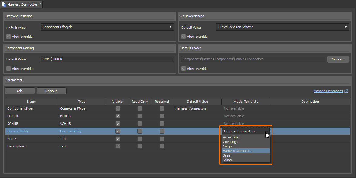
An additional Workspace item type is also available – the Harness Entity Template – allowing for a more streamlined reuse of a defined harness entity model. A harness entity model or template can be referenced through a component template (using the new HarnessEntity parameter). This allows you to quickly create harness components based on specific component (and harness) templates.
When browsing harness components in your Workspace Library through the Components panel, a preview of the related harness entity model is provided (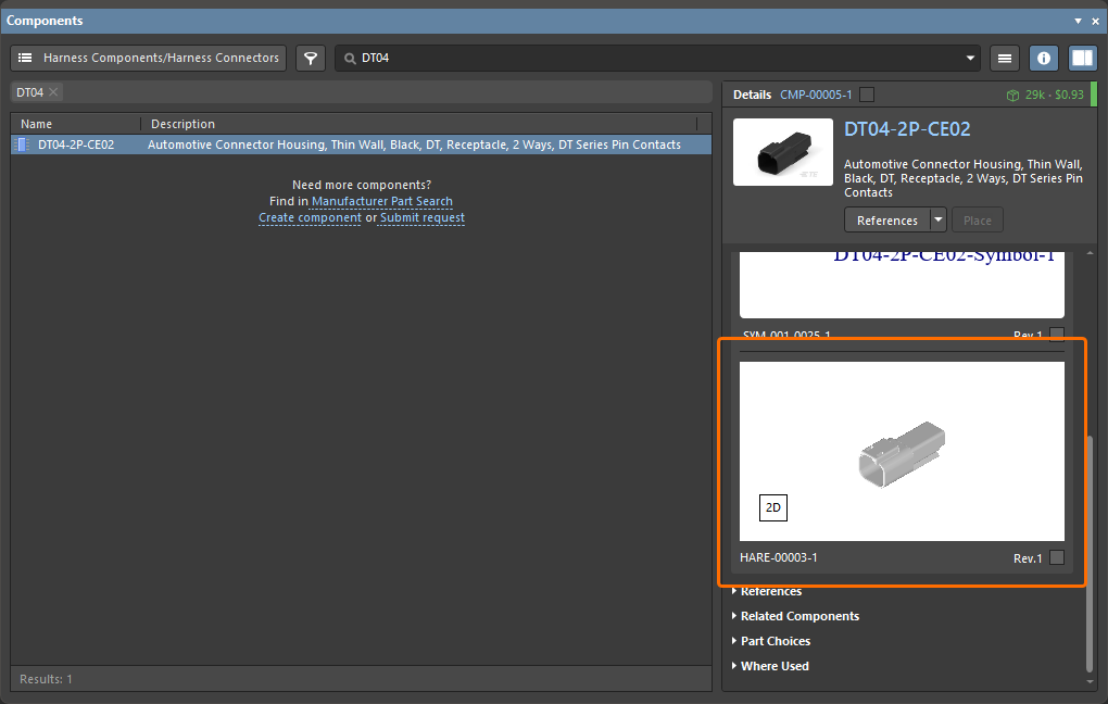 ).
).
For more information, refer to the Creating a Harness Component page.
Harness Library Components – Enhancements in Altium Designer 26.10
Additional Validation Checks for Harness Connectors
Additional validation checks associated with a defined cavity view for a harness connector type harness entity have been added to the Violations Associated with Harness Entities section of the Data Management – Component Rule Checks page of the Preferences dialog:
-
Duplicate Cavity by Name – this violation occurs when the harness entity's cavity model has two or more cavities with the same name.
-
Missing Cavity Crimp – this violation occurs when no crimp is associated with a cavity in the harness entity's cavity model.
-
Missing Cavity Name – this violation occurs when no name is specified for a cavity in the harness entity's cavity model.
-
Missing Cavity Seal – this violation occurs when no seal is associated with a cavity in the harness entity's cavity model.
-
Missing Plug for Cavity Seal – this violation occurs when no plug is assigned to a seal associated with a cavity in the harness entity's cavity model.
Component Rule Check Added to Harness Workspace Item Menus
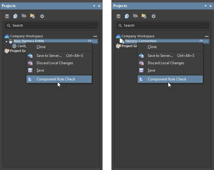
Added the Component Rule Check command to the Projects panel's right-click context menu for both Harness Entity and Harness Entity Template Workspace items.
Restricted Seal Assignment in Cavity Models
When adding an associated seal to a cavity through the Properties panel (with that cavity selected in the Cavity Model editor), you can now only add one type of seal. If an Individual type seal is assigned to a cavity, it is not possible to assign an Interface type seal, and vice-versa.
Added Place Cavity Command to the Main and Right-click Menus
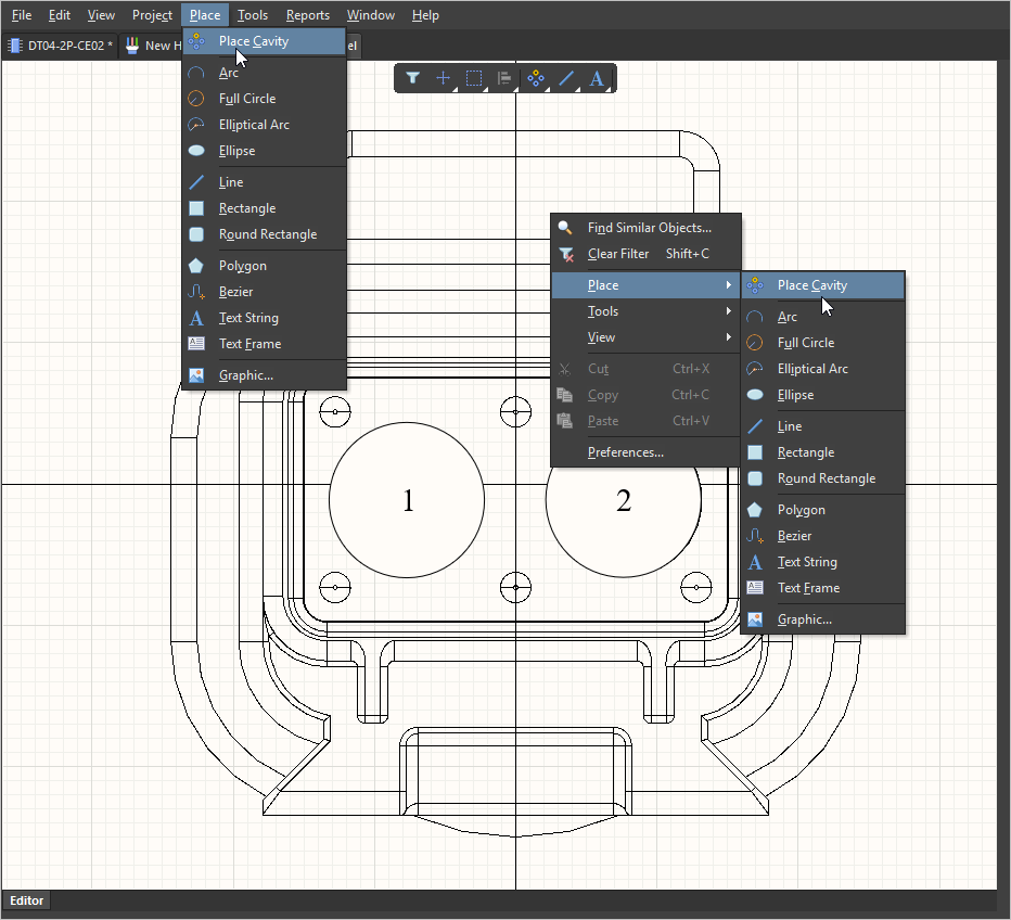
Added the Place Cavity command to the Cavity Model editor's main Place menu, as well as the right-click context menu accessed from within the design space.
Related Components
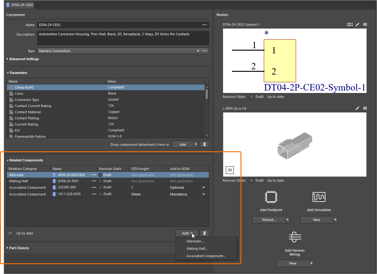
This release brings support for specifying components at the Workspace Library level that are related to a defined PCB or Harness component. A new section is presented – Related Components – with which to do so when defining a component through the Component editor (in Single Component Editing and Batch Component Editing modes).
Add one or more of the following entries as required:
-
Alternate – a replacement component that can be used in place of this defined component (driven by the BOM).
-
Mating Half – this entry is in place for future use when defining two halves of an inline harness connector defined on a multi-board schematic.
-
Associated Component – a component associated with the component being defined. When defining a PCB component for example, this could be a nut, screw, spacer, etc. When defining a Harness component, this could be a backshell, wedgelock, etc. You also have the ability to specify quantity/length and inclusion into the BOM as either Optional or Mandatory.
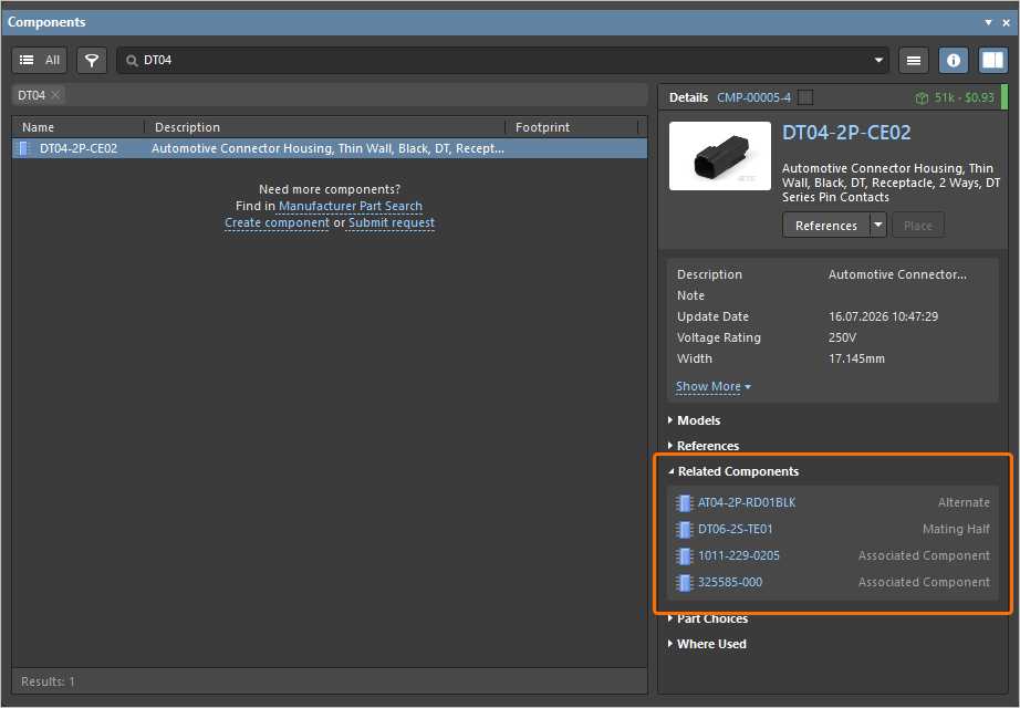
When browsing components in your Workspace Library through the Components panel, a new section for Related Components is provided.
For more information, refer to the Single Component Editing and Batch Component Editing pages.
Related Components – Enhancements in Altium Designer 26.10
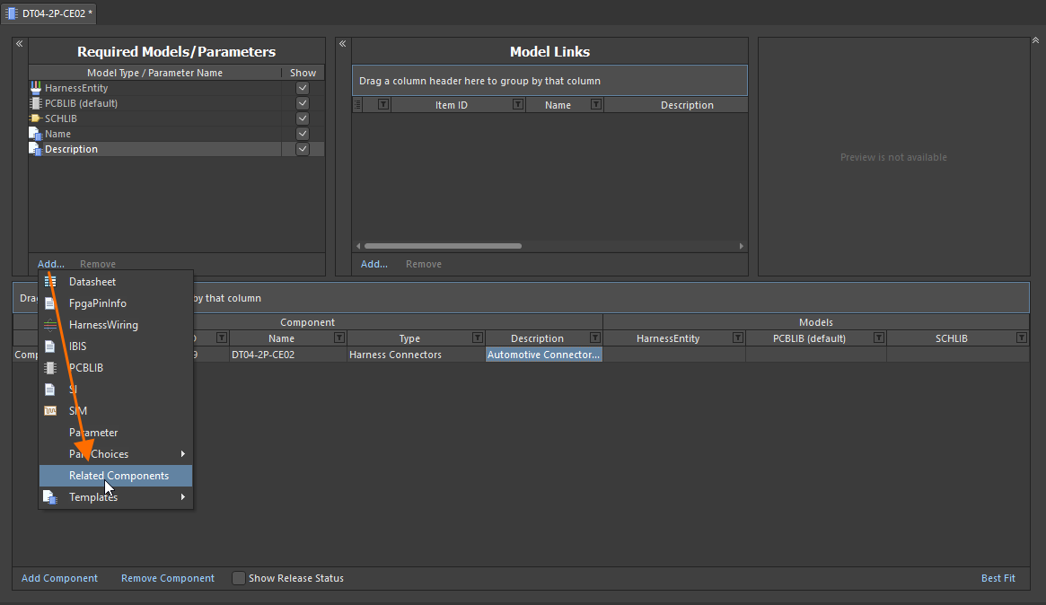
This release extends the functionality of this area with support for specifying, at the Workspace Library level, related components for a PCB or Harness component, when defining that component through the Component editor in Batch Component Editing mode.
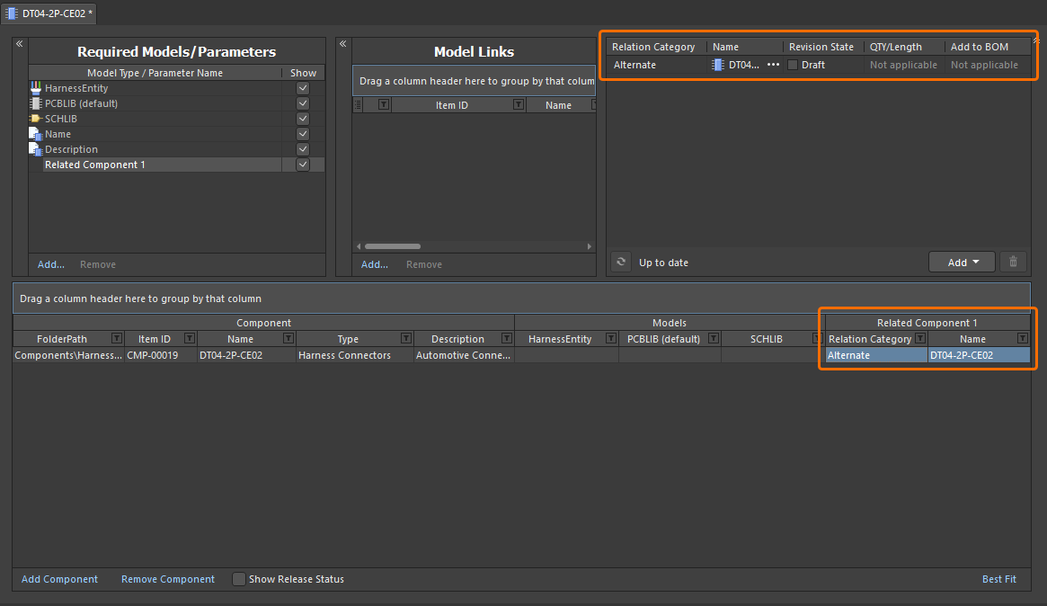
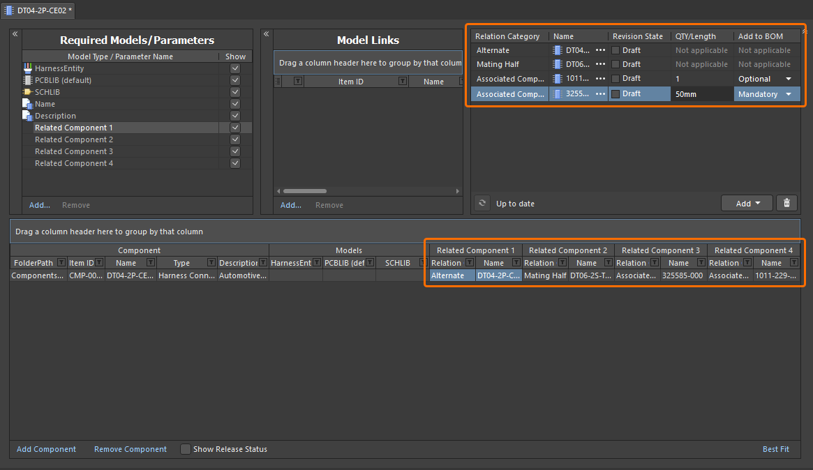
A Related Components entry is now available on the Add menu associated with the Required Models/Parameters region. When added and its visibility enabled, an initial entry (Related Component 1) will appear in the main grid. Click in a cell to access a main configuration region at the top-right of the editor, with which to add the related entities (Alternate, Mating Half, Associated Component) as required. Each added component will have its own section in the main grid.
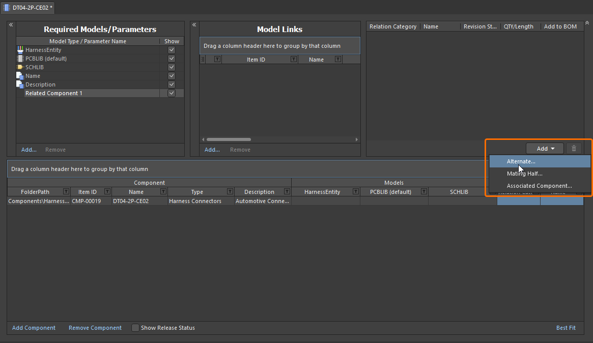
In the top right region of the Component editor, click the  button to add a related component of the required type.
Design Reviews
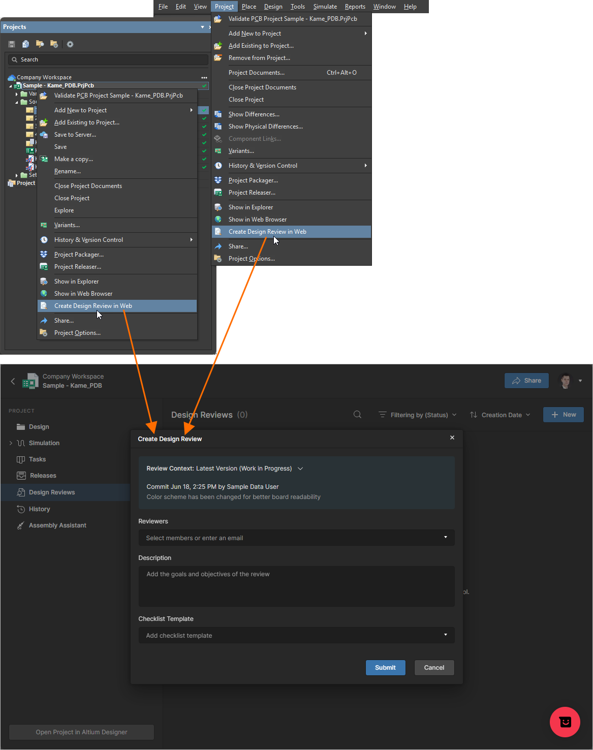
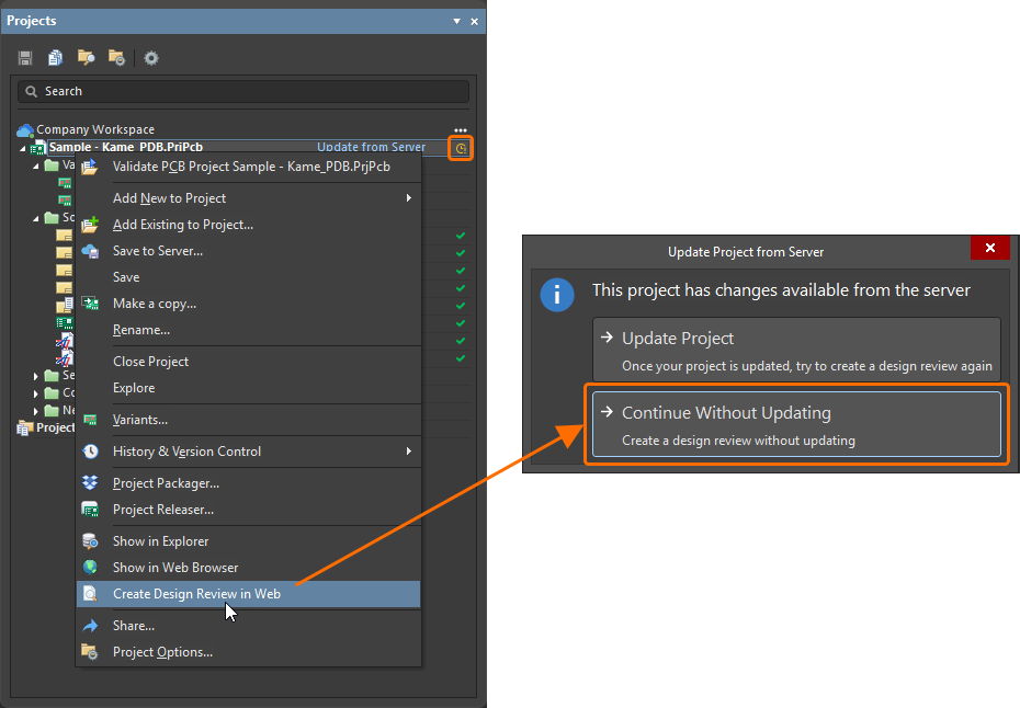
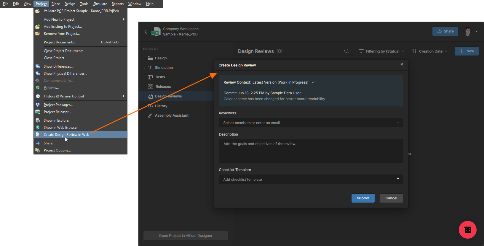
This feature adds the ability to create a design review from within Altium Designer. To create a design review, select Create Design Review in Web from the Project menu or the right-click menu of a project entry in the Projects panel. When the option is clicked, the interface opens in which you can access the Design Reviews page for the project in the Workspace's browser-based interface. The Create Design Review window opens in which you can define reviewers, description and which checklist template is to be used.
Once created, in Altium Designer your active design reviews – for which you are a defined reviewer – will be accessible from a new Design Review page within the project’s Share dialog. You can also initiate design review creation from here.
In addition, if a design review process (with workflow) has been defined and made active through the Workspace, it will become available to you under Altium Designer’s Project » Project Activities sub-menu. If such a process-based workflow is available, you will not be able to initiate design review creation from the Share dialog.
For more information about design reviews, refer to the Sharing a Design page.
Design Reviews – Enhancements in Altium Designer 26.10
Creating a Review for Non-saved and Out-of-date Projects
It is now possible to create a review if you have made local changes to the project, without saving them first.
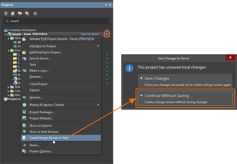
Also, if a later version of the project exists in the Workspace, you can now create a review without having to update your local version first.
Creating a Review from the Main Menus
The Create Design Review in Web command is now available from Altium Designer's main Project menu.
Selectable Harness Source within Multi-board Design
This feature gives you the ability to select the harness design project to be used as the source for a harness connection in a multi-board design, bringing logical connectivity to the latter. With a harness connection selected on a multi-board schematic, you can now choose the required project from the Harness Project drop-down in the Source region of the Properties panel.
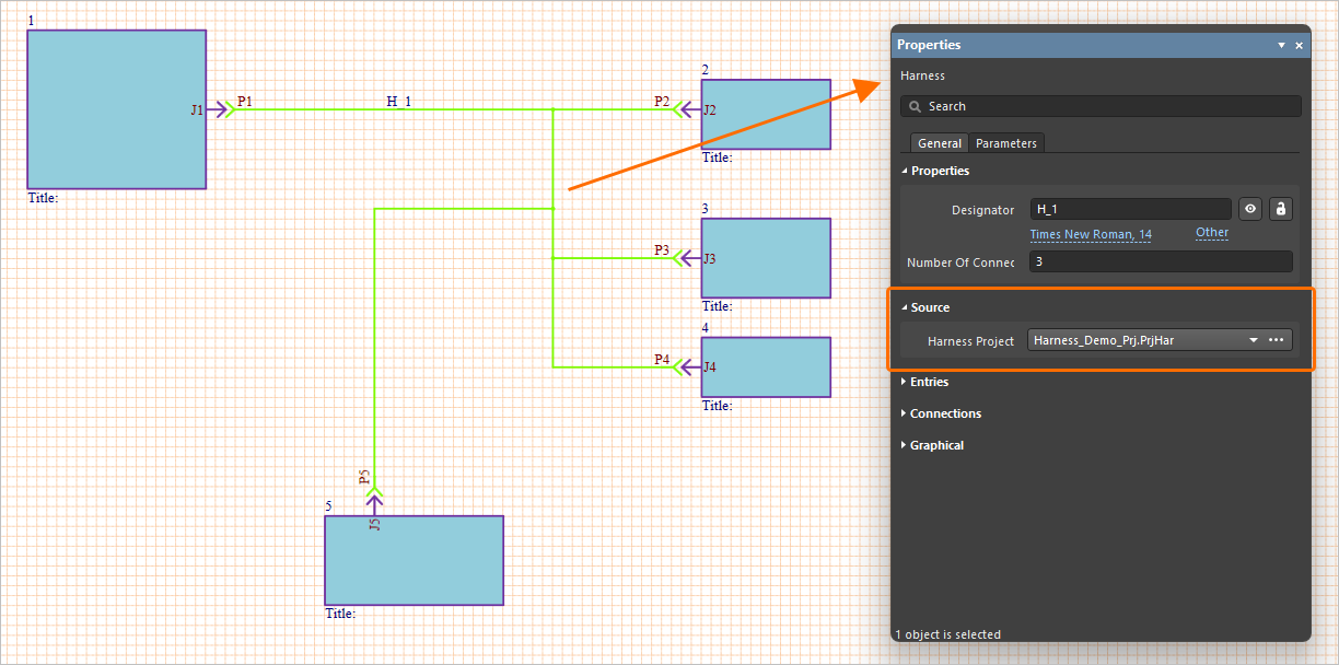
Additionally, you can use the same source harness project for multiple harness connections in the multi-board design. In other words, you can freely define one or more instances of the same harness in your multi-board design. Note that this is analogous to multi-channel in a PCB design, but this is multi-harness in a multi-board design! You no longer need to create a separate harness project per connection with all BOM-related information efficiently taken from one wiring diagram in a single harness design source.
Also, support for the seamless bidirectional synchronization of information between the multi-board schematic and the harness wiring diagram allows the two domains to be worked on independently. Changes can be propagated from one domain to the other through a generated ECO using the Design » Import from Child Projects and Design » Update Child Projects commands in the multi-board schematic and the Design » Import Changes From <Multi-board Project> command in the harness wiring diagram.
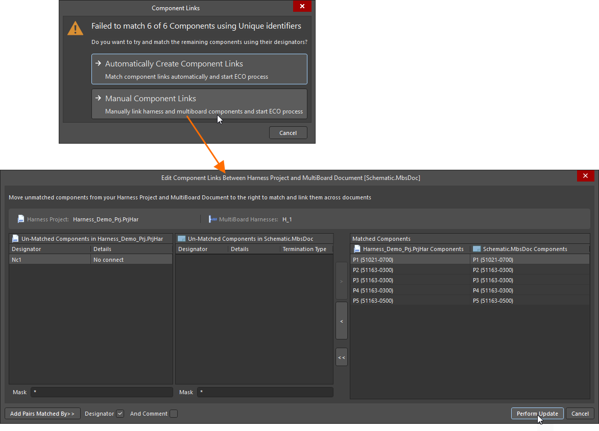
For more information, refer to the Working with Connections page.
Interactive Dynamic Phase Tuning
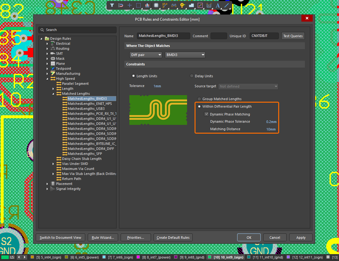
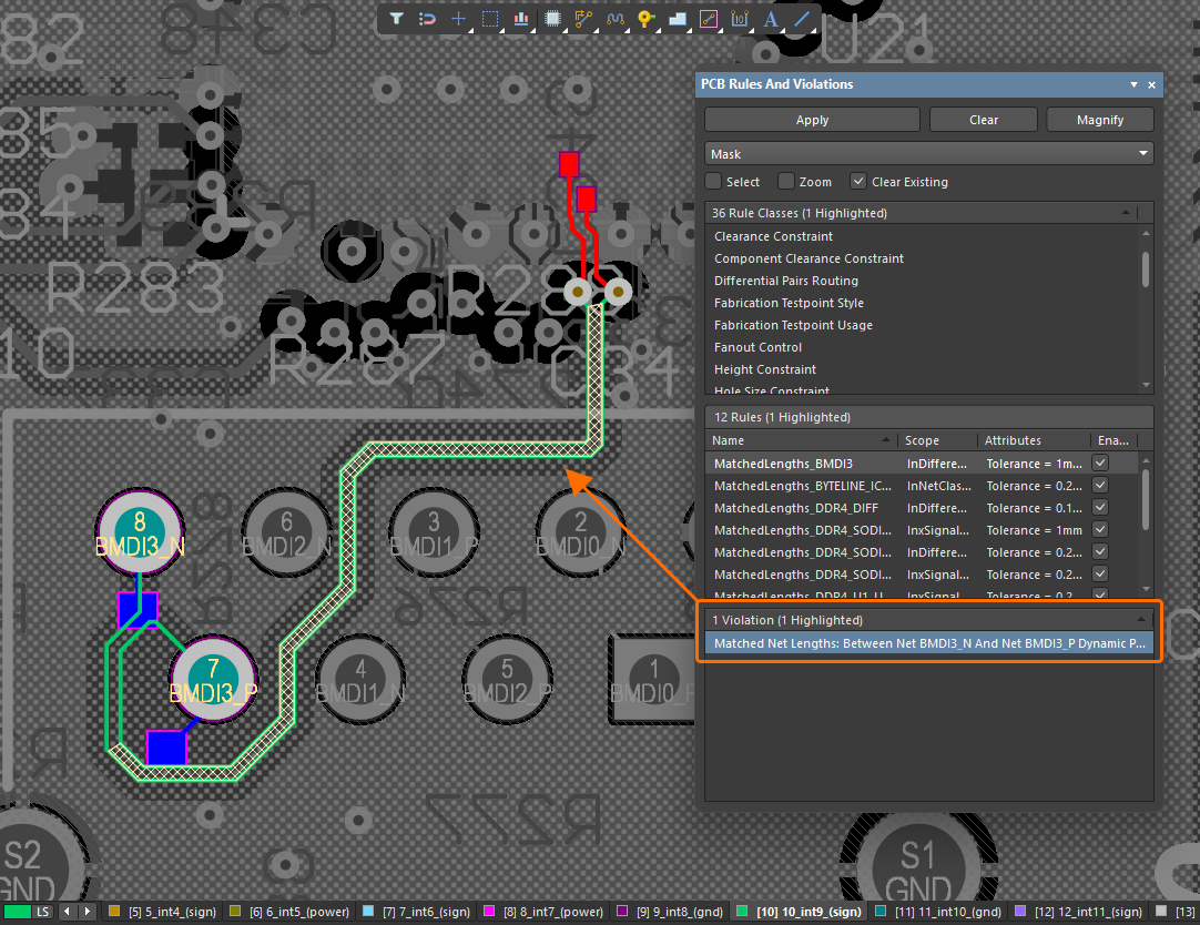
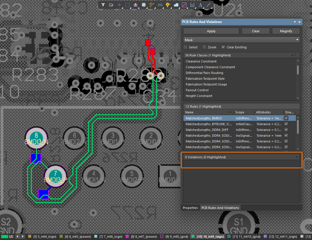
This release adds dynamic phase matching support when manually length tuning a net within a differential pair using the Interactive Length Tuning tool. This facilitates maximum efficiency of differential signal transmission by enabling you to manually equalize the length of the two sides in a differential pair, while also matching the phase along the entire length of the pair.
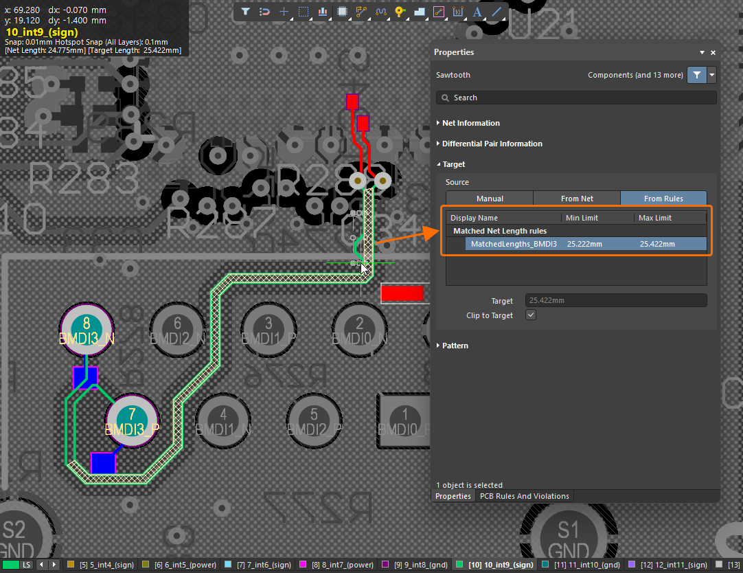
When interactively building the tuning pattern (Tools » Interactive Length Tuning used on a net of a diff pair), the applicable Matched Lengths rule (with the Within Differential Pair Length option enabled and Dynamic Phase Matching enabled and configured) will be listed in the Target region of the Properties panel (Source – From Rules). Whether the pattern is generated or not depends on the position along the track, with the Clip to Target option also observed if enabled (clipping the length to be slightly below the target but within the rule’s defined Dynamic Phase Tolerance), as well as the Length Gauge functioning as expected.
For more information, refer to the Length Tuning page.
Improved Return Path Via Detection
This release adds improved detection of return path vias during design rule checking of a Return Path rule. Stacked and staggered microvias are now considered for use as return path vias.
For a high-speed signal, such vias may be considered for a return path if they connect reference layers for that signal, flowing between layers (if there is only one reference layer for the high speed signal there is nothing to stitch and no return path via is needed), and if the distance between the return path vias, and return path vias and the signal, is not more than the Max Stitch Via Distance defined in the rule.
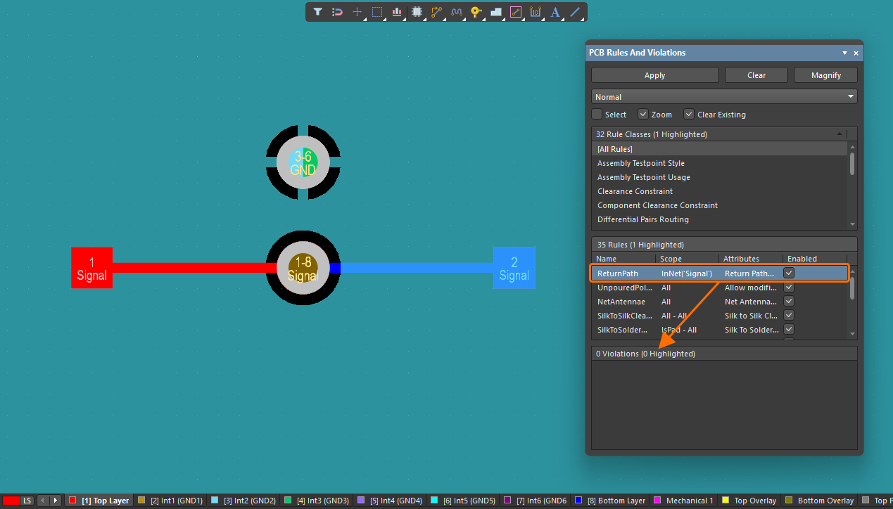
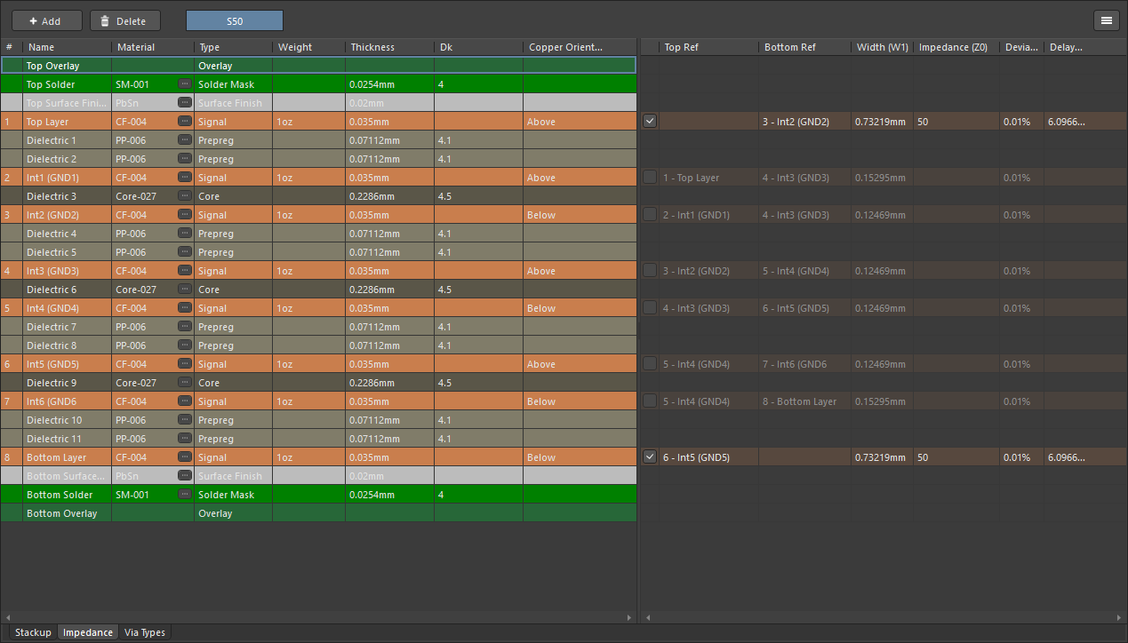
In the example shown below, a stacked microvia is used as a stitch via that connects polygon pours on two reference layers. Since the via electrically connects reference planes where polygon pours exist to facilitate the return path, no Return Path rule DRC violation is detected.
When defining a Return Path rule, additional fields are now available to determine the Reference net or net class. These are supported by the Constraint Manager, DRC and the PCB CoDesign feature.
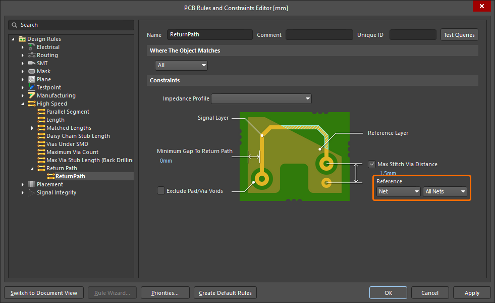
Determining the Reference in the PCB Rules and Constraints Editor dialog
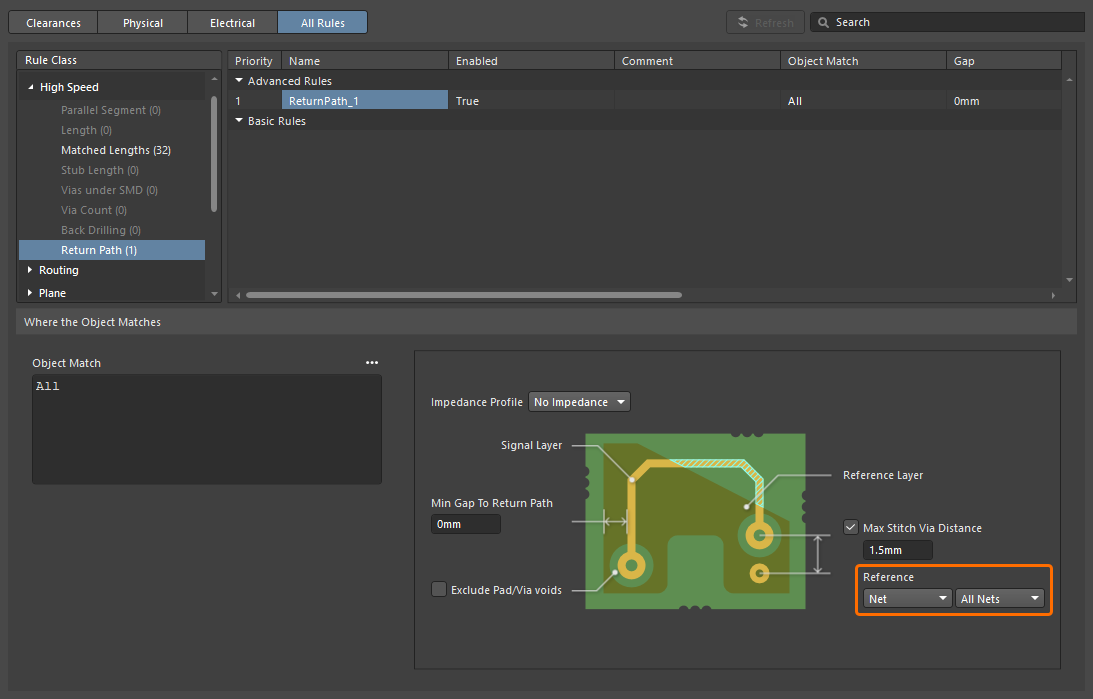
Determining the Reference in the Constraint Manager
For more information, refer to the High Speed Design page.
Streamlined Approach for Overlapping Polygon Pours
This release introduces a streamlined approach for resolving overlapping polygon pours. A lower-priority polygon will only be poured outside of the boundary of a higher-priority polygon that is either completely nested within it or partially overlaps it, resulting in a significant performance using less time to repour polygons.
In the example shown below, a polygon that belongs to net IO_2V5 (green) is a higher-priority polygon and a polygon that belongs to net GND (pink) is a lower-priority polygon, and the IO_2V5 net polygon was poured before the GND net polygon. While there are voids formed by densely placed vias in the IO_2V5 net polygon and the GND net polygon fully overlaps it, these voids are not filled by the GND net polygon because it is a lower-priority polygon.
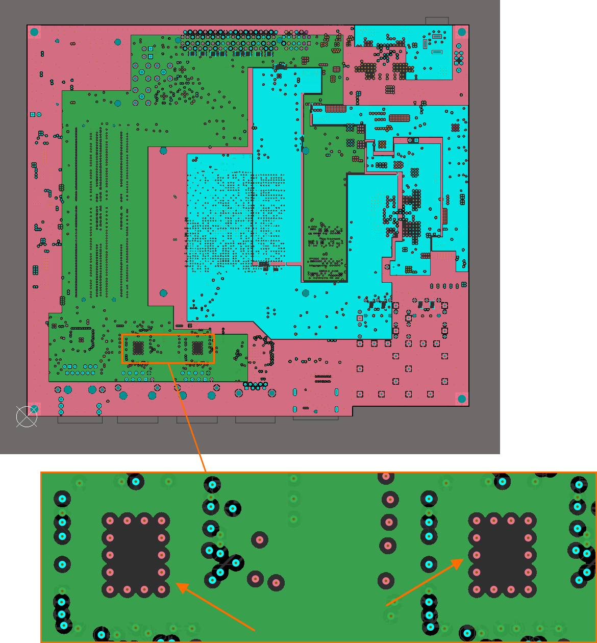
For more information about the configuring the pour order, refer to the Polygons on Signal Layers page.
Rounding for Diff Pair Gap/Width Transitions
This release brings support for automatically adding rounded miters at gap/width transitions during Any Angle diff pair interactive routing or rounded diff pair glossing, particularly at room boundaries.
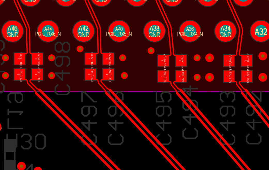
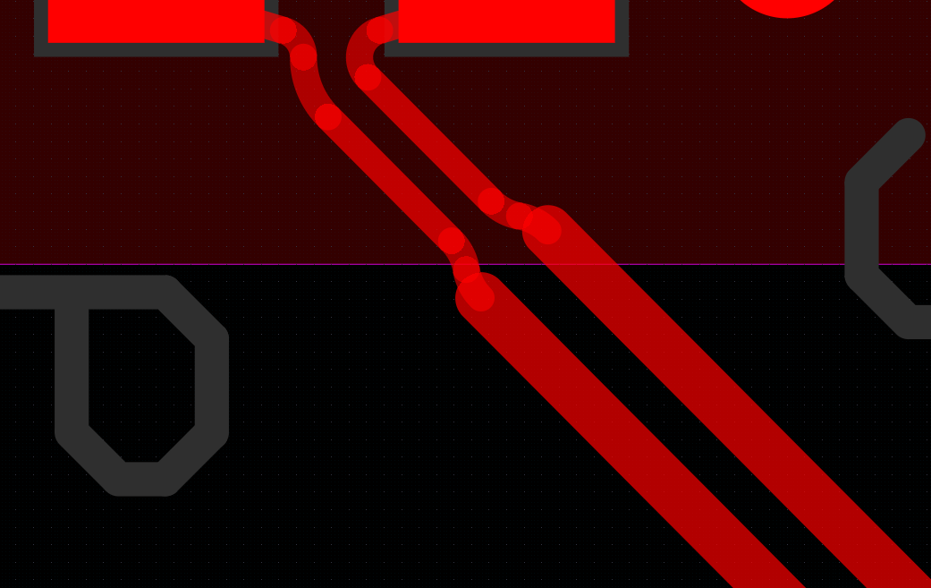
For more information about diff pair routing, refer to the Differential Pair Routing page.
Sawtooth Rounding
You now can apply rounded corners to sawtooth patterns when interactive length tuning and interactive diff pair length tuning. In the Rounding field of the Properties panel, enter the desired rounding percentage between 0% (default) and 50% or use the  buttons to decrease or increase the Rounding value per the fixed 5% interval provided in the Step field.
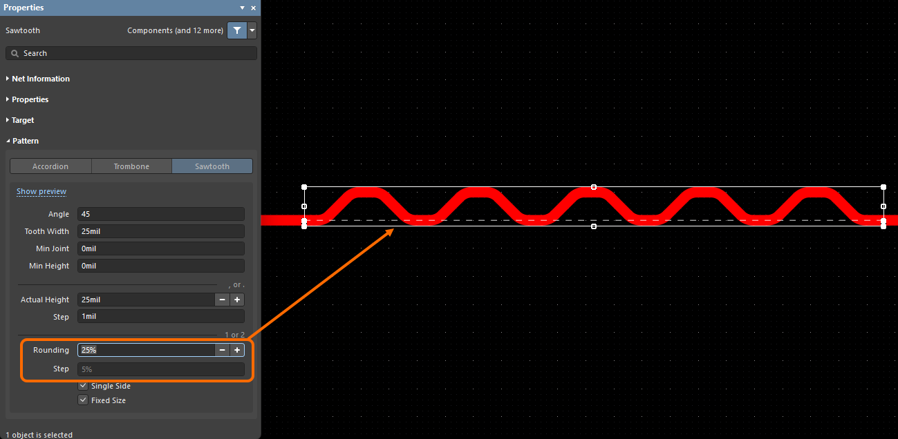
The rounding feature can also be accessed when using the automatic length tuning feature (Route » Automatic Length Tuning). In the Auto Tuning Process dialog that opens after initiating the command, the Rounding and Step options are available on the Within Pair Matching tab.
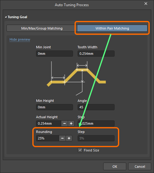
For more information about sawtooth patterns, refer to the Length Tuning page.
3D-MID Export of Tracks to Centerline Curves
To support 5-axis production processes, tracks on the 3D substrate can now be exported as centerline curves when exporting the 3D-MID design into STEP format.
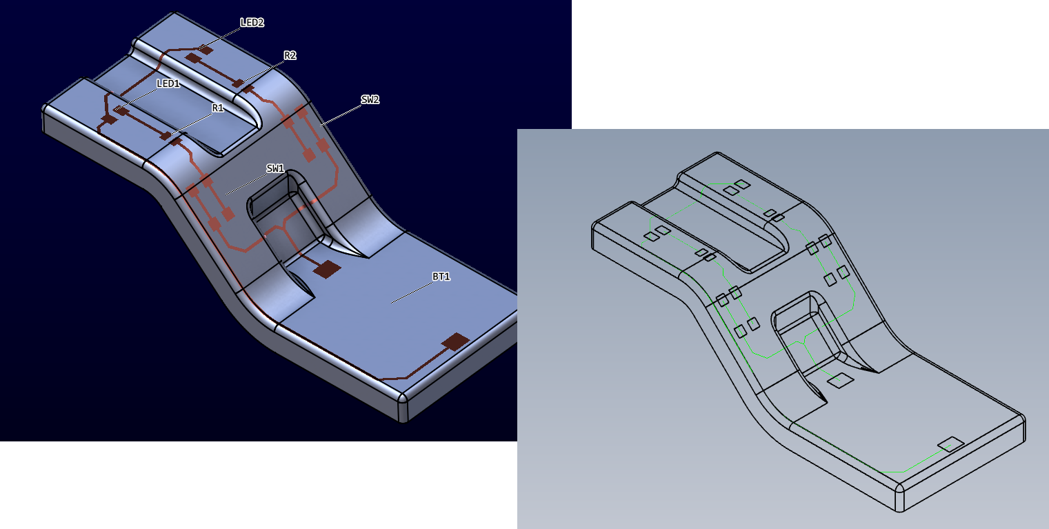
Tracks in the 3D-MID design can be exported into a STEP file as centerline curves. The 3D-MID document is shown on the left and the exported STEP file is shown on the right, with track centerlines highlighted in green.
Also, when exporting a 3D-MID design into any available format, a text file (<3DMIDDocumentName>_tracks.txt) is generated in the same folder as the exported 3D-MID file. This text file includes information about the location of each of the tracks in the design, as well as their width and net attributes.
For more information, refer to the 3D-MID Design page.
Automatic Face Filling
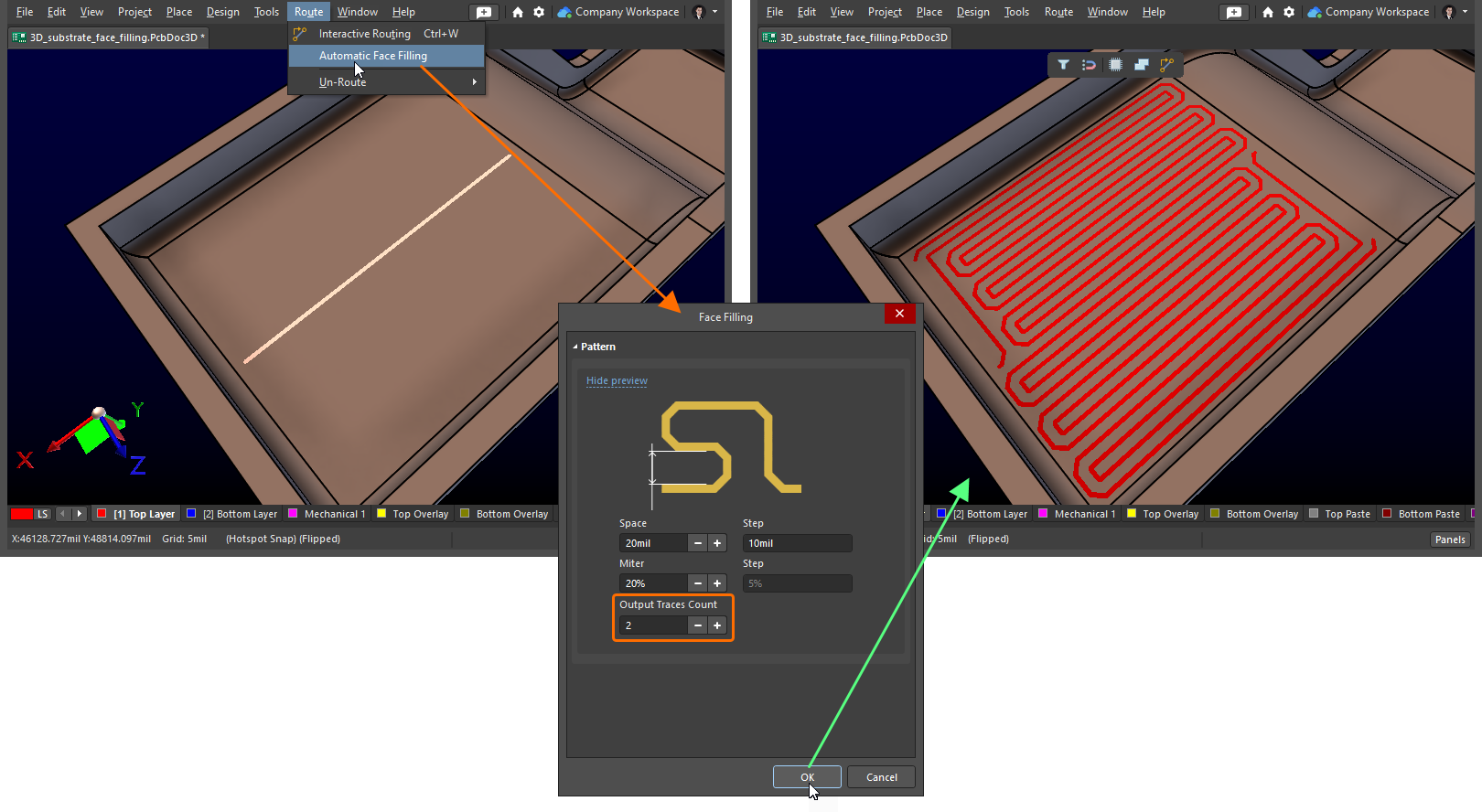
This release delivers a first-step implementation of the ability to fill the faces of the 3D substrate in a 3D-MID design document with a geometric pattern. This functionality is especially aimed at those wanting to quickly create a geometric covering for security purposes, such as a protective mesh for secure payment terminals.
To use this feature, choose the Route » Automatic Face Filling command from the main menus when a trace is selected. Use the Face Filling dialog that opens to configure the geometry properties of the pattern and the number of traces to be used in the creation of the geometric pattern, and then click OK. The surface will be filled with a pattern whose overall height equals the length of the initial track and which extends perpendicular to the track up to surface boundaries while avoiding obstacles.
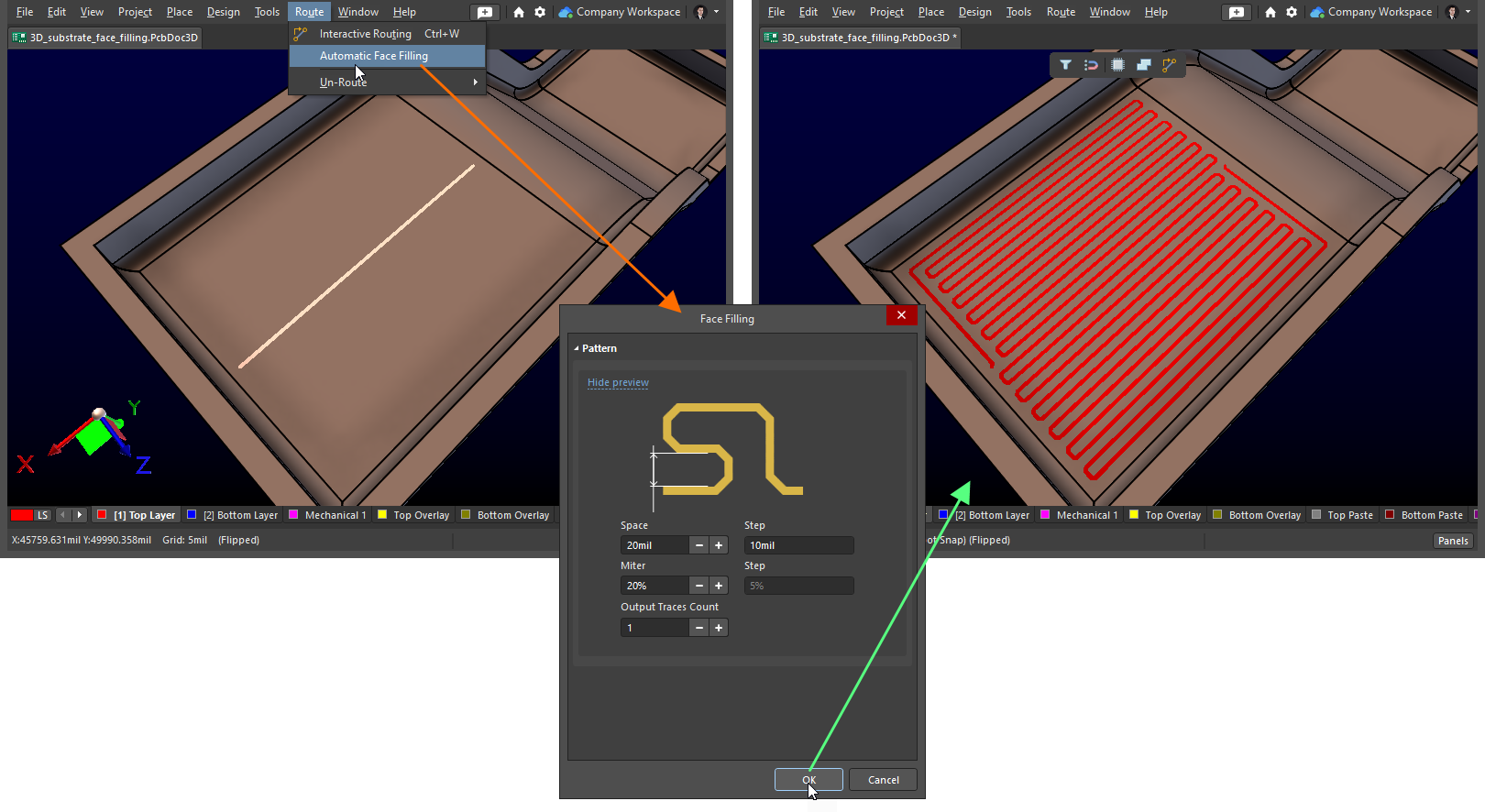
For more information, refer to the 3D-MID Design page.
Automatic Face Filling – Enhancement in Version 25.5
Support for Non-flat Surfaces
This release extends the functionality of the automatic face filling feature with the ability to use it on any surface (not just flat). In order to use this feature, the 3DLayout.FaceFilling.AllowAllSurfaces option must be enabled in the Advanced Settings dialog.
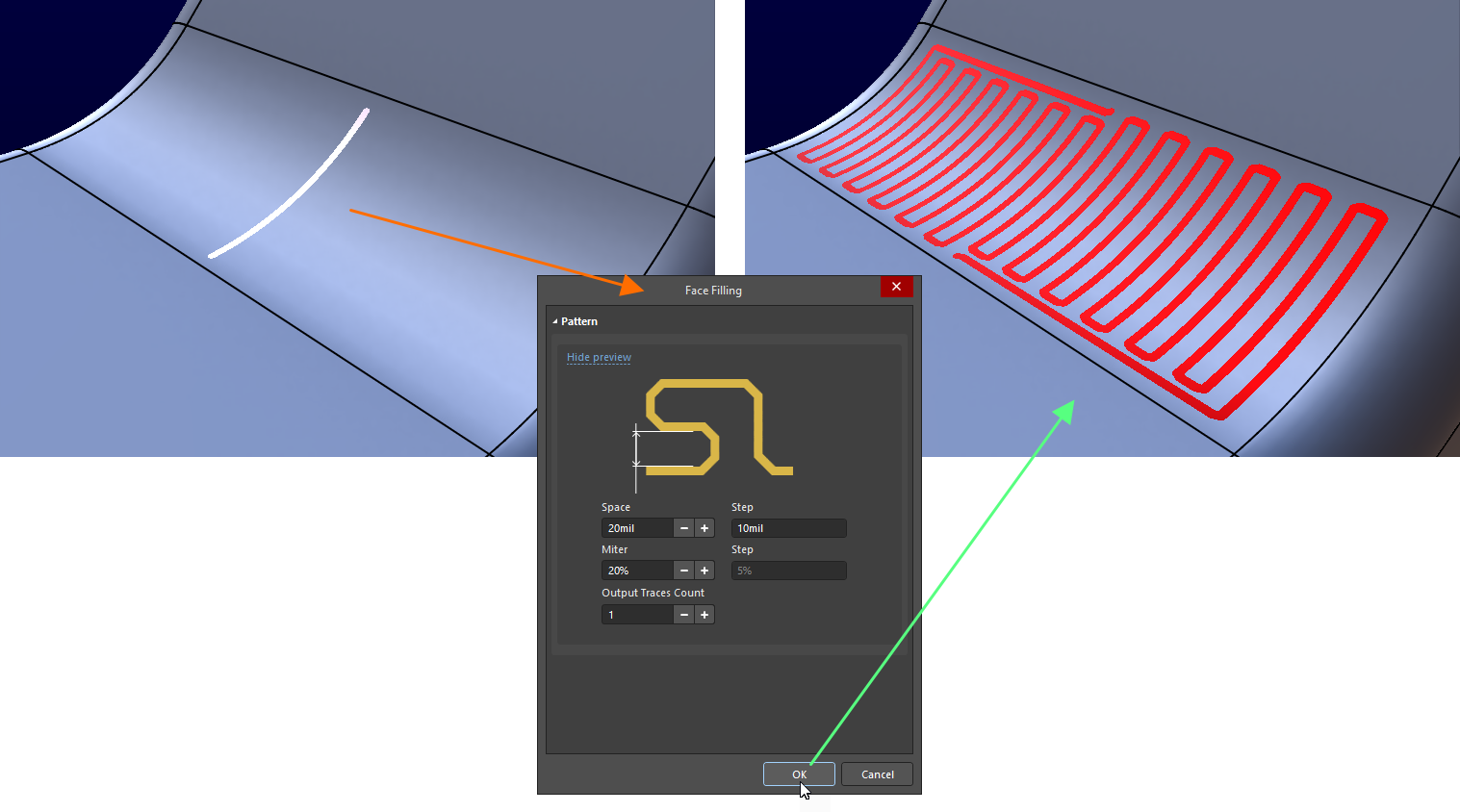
An example of using the automatic face filling feature on a cylindrical surface
Automatic Face Filling – Enhancement in Version 25.4
Support for Multiple Output Traces
This release extends the functionality of the automatic face filling feature with support for defining the number of traces to be used in the creation of the geometric pattern, when automatically filling a face of the 3D substrate. In the Face Filling dialog, use the new Output Traces Count option to define the desired number of output traces.
Dynamic Re-route on Component Drag
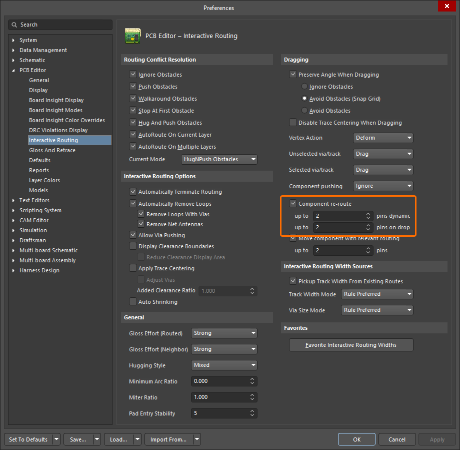
Additional options are available in the PCB Editor – Interactive Routing page of the Preferences dialog that help to better control re-routing. When the Component re-route option is enabled, in the fields below, you can define the maximum number of connections that a moving component can have before the routing engine will no longer attempt to re-route. The up to xx pins dynamic field is used to specify the maximum number during movement (i.e., dynamically re-route as the component is being moved). Use the up to xx pins on drop field to specify the maximum number at final placement (i.e., when the component is 'dropped' into final position).
For more information, refer to the Modifying Existing Routes page.
Using Polygons on Power Planes
Traditionally, a PCB power plane is designed as a negative, that is, the objects placed on a power plane layer become voids in the copper when the board is fabricated. This approach is used because it is more efficient to generate the output data this way, as the bulk of a plane layer is normally copper; voids in the copper are only needed in specific locations such as around non-connected pads, or as separation voids when the plane is divided into different voltage regions.
As part of improving support for more complex power plane design, it is now possible to define power planes as polygons. Working in this mode does not affect the approach to designing a power plane; they are still defined in the negative – so placing an object creates a void in the copper, and they continue to be split into separate regions by placing a split line.
The advantage of using polygons is that copper islands, narrow necks and dead copper can automatically be detected and removed.
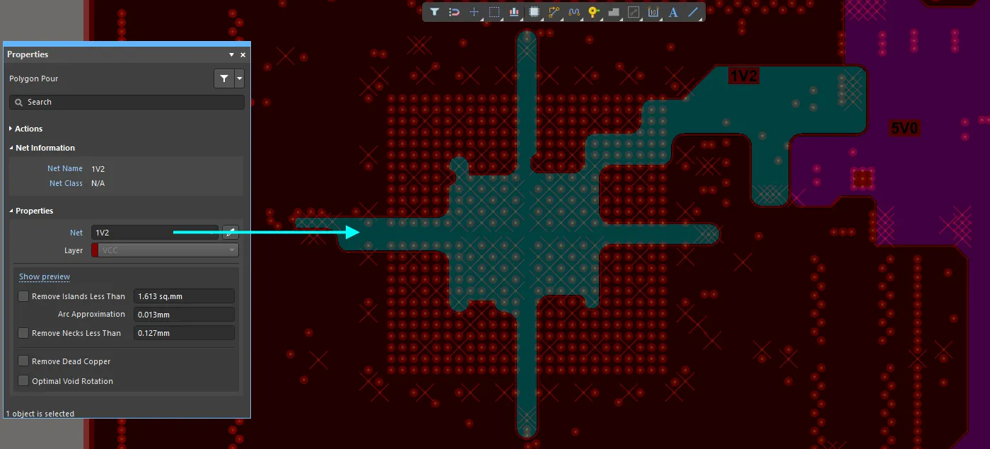
Although the layer appears the same, using polygons on the plane layers allows for more comprehensive checking of the integrity of the copper.
Notes about the Polygons on Plane mode:
- After enabling the option, review each plane layer and repour the plane polygon(s) with the polygon options configured to suit your design needs.
- Connections and Clearances for plane layers are defined by the PlaneConnect and PlaneClearance design rules.
- After modifying a plane (connect or clearance) design rule, repour at least one polygon on each plane layer, to update the connections/clearances on that layer.
- Edits made on a plane layer, such as modifying the location of a split line, cause an automatic repour of polygons on that plane layer.
For more information, refer to the Internal Power & Split Planes page.
Via Annular Rings on Terminating Plane Layers
An annular ring has always been included on a signal-terminating layer. This release includes the introduction of an annular ring shape when the terminating layer (the first and/or last layer of the via) is a plane layer, regardless of whether the via on that layer is being connected.
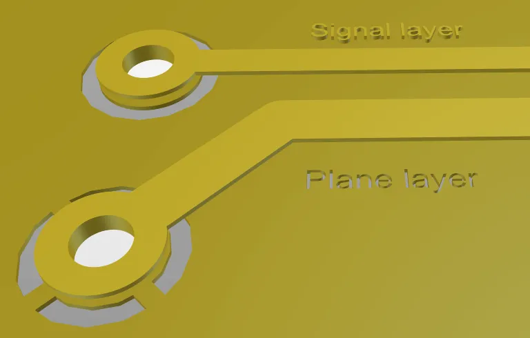 Terminating plane layers now include an annular ring for all vias.
For more information, refer to the Internal Power & Split Planes page.
Compact Parameter Auto-Positioning for Discrete Parts
This release improves the positioning of parameters for components placed on a schematic sheet by introducing a compact auto-positioning option for 2-pin discrete components (when horizontally oriented). Enabled using the new Compact Autoposition for Discrete Parts option on the Schematic – General page of the Preferences dialog, this feature acts solely on the Designator and Value parameters to place them tightly around the second pin of the device symbol. All other parameters remain untouched in their placed locations.
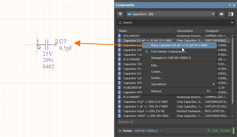
Same-Net Clearance Rule Between Polygon Pours and Pads/Vias
Added support to Design Rule Checking (DRC) for applying and observing a defined same-net clearance constraint in the following cases:
-
between polygon pours
-
between polygon pours and pads/vias (where the pad/vias do not have a direct physical connection to the pour and are located in or outside of the pour area).
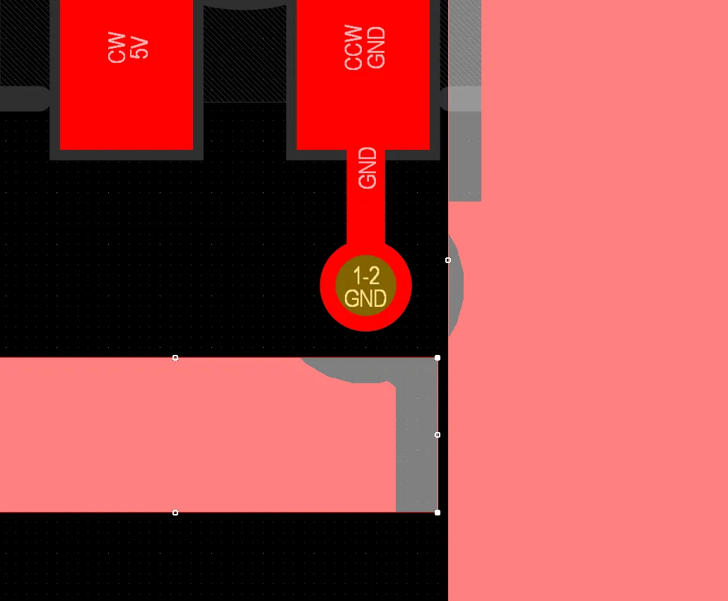
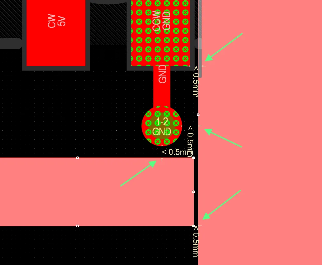
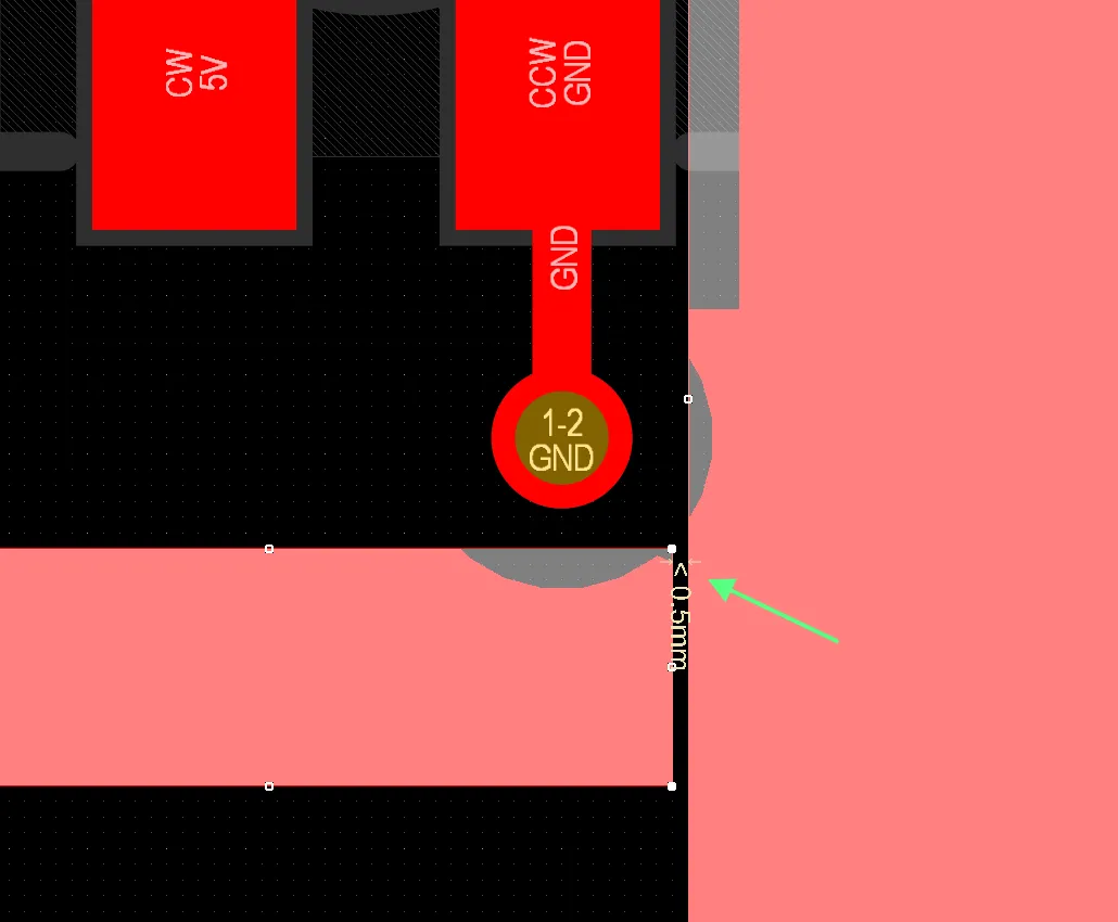
Also, the pouring of polygons now adheres to defined same-net clearance rules between a polygon pour and a pad/via. When there is a clearance constraint between a pad/via and a polygon pour of the same net, the polygon pour will be poured to maintain this constraint (provided the pour is in Don't Pour Over Same Net Objects or Pour Over Same Net Polygons Only pouring mode).
|
A PCB with polygon pours in Don't Pour Over Same Net Objects pouring mode. The polygons are poured to maintain the clearance constraint between polygons of the same net and between polygons and pads/vias of the same net. The same PCB with polygon pours in Pour Over All Same Net Objects pouring mode. The polygons are poured without maintaining the clearance constraint, and constraint violations are detected between polygons of the same net and between polygons and pads/vias of the same net. The same PCB with polygon pours in Pour Over Same Net Polygons Only pouring mode. The polygons are poured to maintain the clearance constraint only between polygons and pads/vias of the same net, and a constraint violation is detected between polygons of the same net. |
Same-Net Clearance Rule Between Polygon Pours and Pads/Vias – Enhancement in Version 24.5
Pouring Polygons Around Same-Net Pads and Vias
The pouring of polygons now adheres to defined same-net clearance rules between a polygon pour and a pad/via. When there is a clearance constraint between a pad/via and a polygon pour of the same net, the polygon pour will be poured to maintain this constraint (provided the pour is in Don't Pour Over Same Net Objects or Pour Over Same Net Polygons Only pouring mode).
Export an Image of the Power Network Tree – Power Analyzer by Keysight
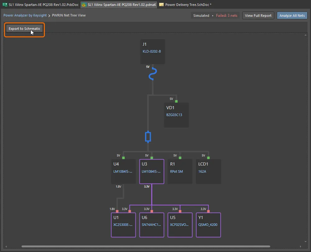
The Power Analyzer by Keysight release 1.0.7 includes a new feature that helps to document the analysis of the power network in your design.
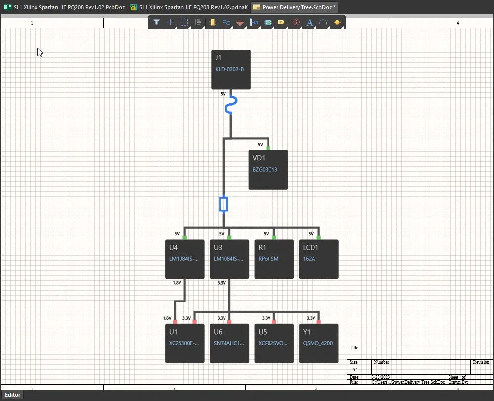
When you are examining the Tree View in the Power Analyzer by Keysight document (<ProjectName>.pdnaK), click the  button to export a PNG-format image of the entire network tree to a new schematic document. The schematic is automatically titled
 Power Delivery Tree.SchDoc.
|
To help with the documentation process, an image of the entire Power Network can be exported directly to a schematic sheet. To help with the documentation process, an image of the entire Power Network can be exported directly to a schematic sheet. |
Defining Clearance By Layer
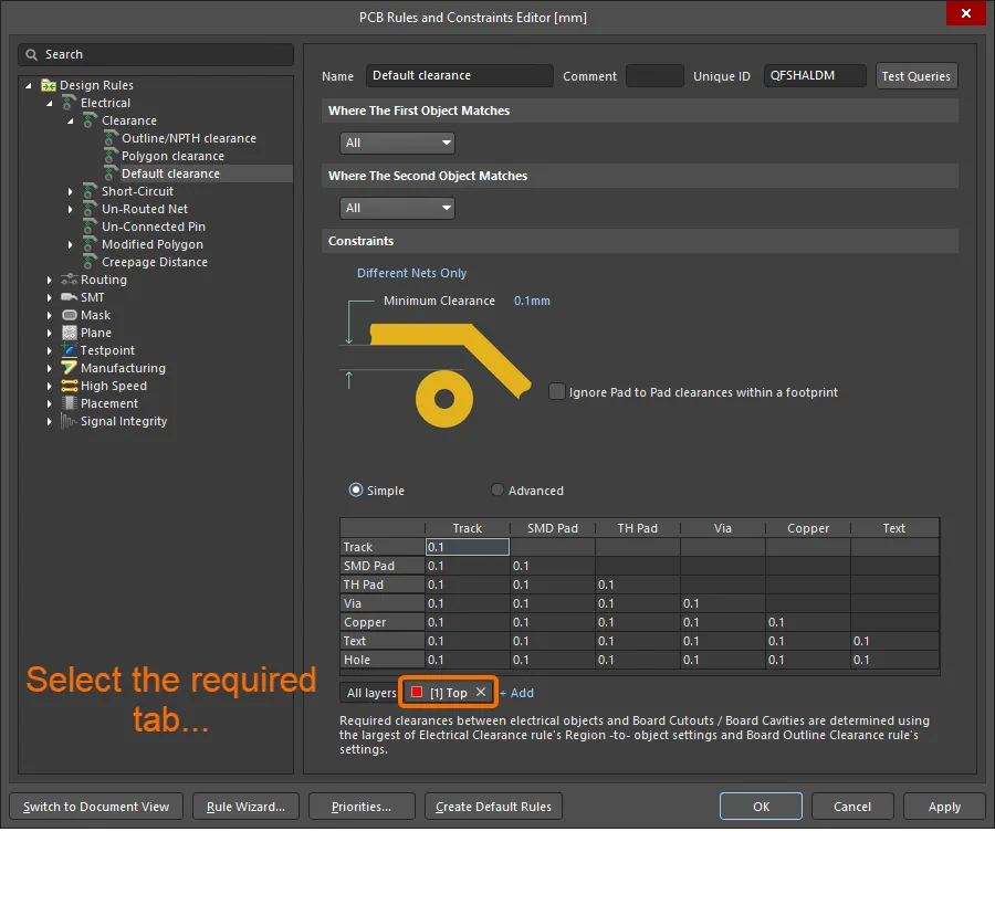
When designing a PCB, you may need to adjust the clearances between primitives differently (track, via, polygon, etc.) depending on the layer. For example, the clearance between copper tracks on inner layers must be 35 µm, and only 18 µm is needed for outer layers. Another example is the clearance between a via or through-hole (multi-layer) pad and other copper objects – if the pad/via has shapes of different sizes on layers, you might need to define different clearances for these layers.
Beginning with this release, you can define the clearances by layer using controls below the clearance matrix in the Constraints region of the Clearance design rule. By default, the All Layers tab is shown, and the matrix is used to configure clearances between objects on all signal layers. Click the Add control, then select an entry of the specific signal layer or the group of layers (outer/inner layers) for which you want to configure the clearances and then configure the values of clearances on the added tab as required.
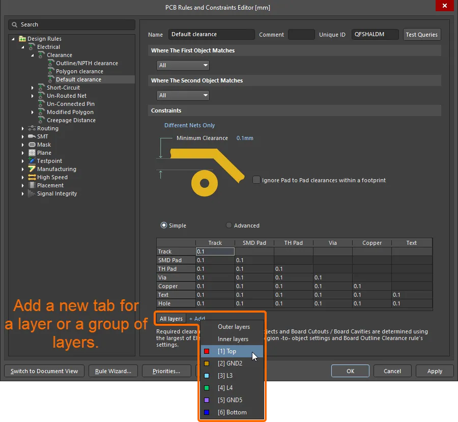
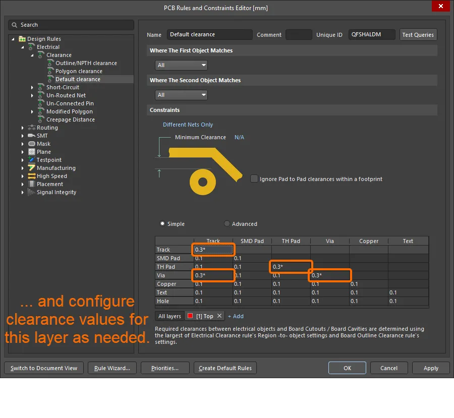
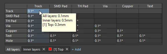
If a cell in the clearance matrix has different values on added layer tabs, an asterisk will display next to the value in that cell on all tabs. Hover the cursor to display a tooltip listing the values of this cell for different layers.
Altium Performance Monitor
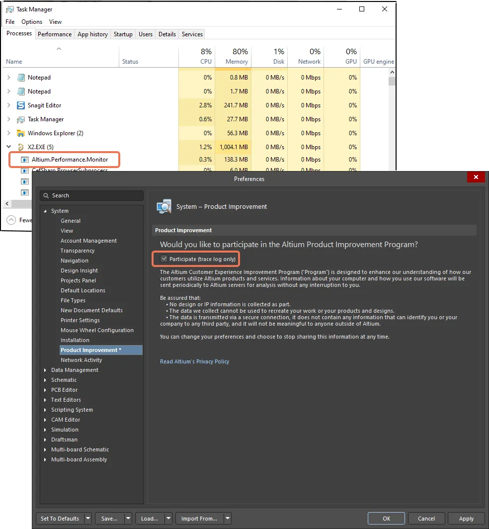
This release includes the Altium Performance Monitor, which monitors your installation of Altium Designer and collects important debugging data in the event of a system freeze (when a process takes longer than it should to execute). Running in the background (Altium.Performance.Monitor) as a distinct process under the main application (X2.exe), if the software ‘hangs’ at any point, the Monitor will gather call stack information, package it to a temporary file, and send the data to Altium for investigation.
Note: This new functionality is part of the Altium Product Improvement Program. Therefore, the Participate option on the System – Product Improvement page of the Preferences dialog must also be enabled.
Additional Features/Functionalities
-
Primitive Delay Cache: A new advanced settings option –
PCB.Performance.UseNetDelayCalculationCache– is available in the Advanced Settings dialog with this release that saves/loads the calculated relative delay for each type of primitive to/from cache. This improves the performance in calculating the delay when reopening a design and selecting a primitive for the first time. -
Git Fast Clone: A new advanced settings option –
VCS.GitFastClone– is available in the Advanced Settings dialog with this release which, when enabled, improves the speed when opening a Git-based project from a connected Workspace. A special server endpoint is used to make the underlying 'git clone' operation faster (to obtain the local repository for an existing (remote) Git repository). In tests with a design project of 500 MB, the opening time was less than a minute with the option enabled (compared with 4-5 minutes with the option disabled).