
Routing Rule Types
The design rules of the Routing category are described below.

The Routing category of design rules
Learn more about Defining, Scoping & Managing PCB Design Rules.
Learn more about Interactive Routing.
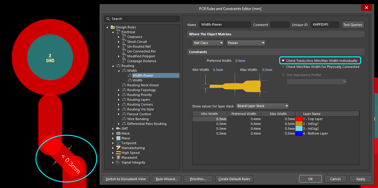
Width
This constraint defines the width of tracks placed on the copper (signal) layers during interactive routing and autorouting. It also defines the allowed widths during on-line and batch DRC. A board will typically have multiple Width rules, targeting all nets (the lowest priority Width rule), specific nets, and classes of nets.
Constraints
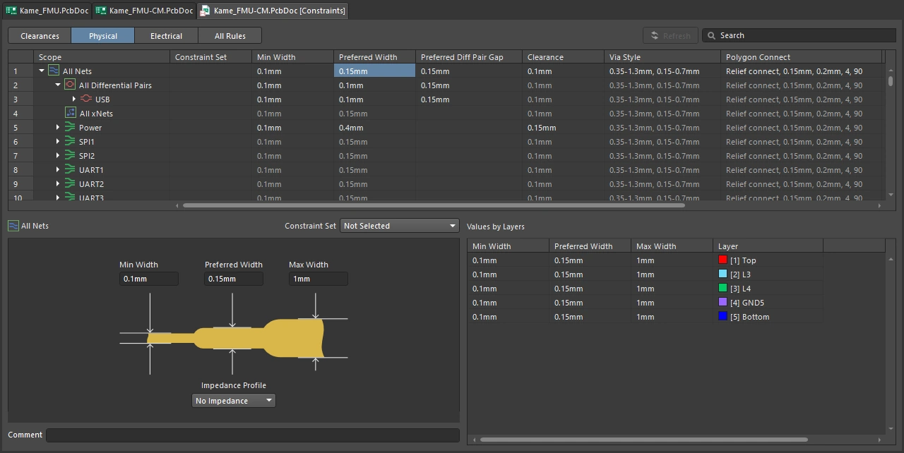
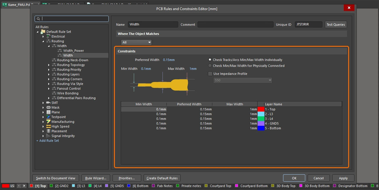
Width Constraint Settings
| Default Rule | Required |
| Preferred Width | Specifies the preferred width to be used for tracks when routing the board. |
| Min Width | Specifies the minimum permissible width to be used for tracks when routing the board. |
| Max Width | Specifies the maximum permissible width to be used for tracks when routing the board. |
| Check Tracks/Arcs Min/Max Width Individually | For each route in the net targeted by the rule, check that the width of each individual track and arc falls within the minimum and maximum range ( |
| Check Min/Max Width for Physically Connected | For each route in the net targeted by the rule, check that the actual width of the routed copper formed by the combination of tracks, arcs, fills, pads, and vias falls within the minimum and maximum range (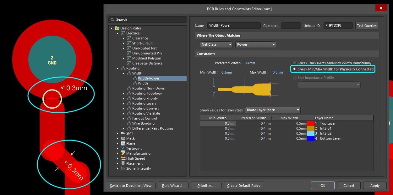 ). ). |
| Use Impedance Profile | This option becomes available when at least one impedance profile is defined in the Layer Stack Manager. When enabled, use the drop-down to select the impedance profile desired. When the rule is configured in this mode, the Preferred Width required on each routing layer is calculated as part of the specified impedance profile (Min Width and Max Width values will also be set to this value when the option is enabled). Once the rule is defined, as you route a net that falls under the scope of the rule, the track width will automatically be set to the width required to meet the specified impedance for that layer. When this option is enabled, the Preferred Width cannot be edited in the rule, but the Min Width and Max Width values can. Learn more about Configuring the Layer Stack for Controlled Impedance Routing. |
| Show values for layer stack | This option appears when multiple layer stacks are defined in the Layer Stack Manager. If the board includes multiple layer stacks, then the Width Constraints must be configured for each stack, using either the all-layer fields above the image or the layer-specific fields in the Layer Attributes Table ( Learn more about Defining and Configuring Substacks. |
| Layer Attributes Table | The grid region at the bottom of the dialog displays all signal layers defined in the layer stack unless the Use Impedance Profile option is enabled. If this option is enabled, then only the layers available as part of the selected impedance profile will be displayed. The grid displays the minimum, maximum and preferred routing widths and other layer-specific information. The routing width fields can be set globally by defining the values in the constraint fields above the image or individually by typing values directly into the table. When the Use Impedance Profile option is enabled, the required width entries will be automatically calculated and entered for each layer in the table. In this mode, the Preferred Width values cannot be edited, but the Min Width and Max Width values can. |
| Defining the Widths in a Differential Pair | The width of each net in a differential pair is monitored by the applicable Differential Pairs Routing rule. |
| Rule Application |
|
 ).
).
 ).
).Learn more about changing the width during interactive routing.
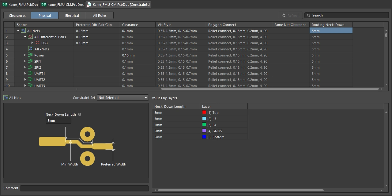
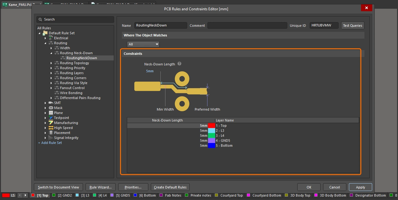
Routing Neck-Down
It is not uncommon for a net to be routed at different widths as the routing travels across the board. For example, routing into or out of a BGA often requires escape routes that are narrower than the preferred width routes allowed by the applied impedance profile. This constraint lets you define the maximum allowed total length of such narrower traces so that the route still delivers the required impedance.
Constraints
Routing Neck-Down Settings
| Default Rule | Not required. |
| Neck-Down Length | Specifies the maximum allowed length of continuous routes (in each net scoped by the rule) whose width is between the Min Width and Preferred Width defined by the applicable Routing Width rule. Alternatively, use the grid to define the allowed length per layer basis. |
| Rule Application | Enable the Routing Neck-Down rule type check for online and/or batch checking in the Design Rule Checker dialog to detect violations of the Routing Neck-Down rules in corresponding DRC modes. Detected rule violations will be marked with a hatched pattern on corresponding traces in the design space. |
Learn more about automatic neck-down during routing.
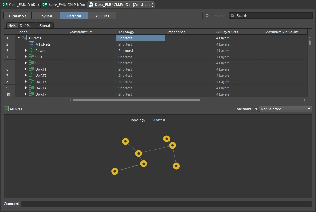
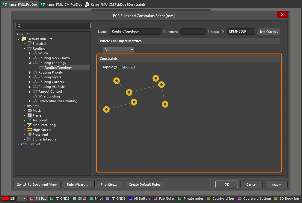
Routing Topology
This constraint specifies the topology to be employed when routing nets on the board. The topology of a net is the arrangement or pattern of the pin-to-pin connections. By default, pin-to-pin connections of each net are arranged to give the Shortest overall connection length. When this topology is applied it is re-analyzed and updated each time a component is moved.
A specific topology is applied to a net for various reasons; for high-speed designs where signal reflections must be minimized the net is arranged with a daisy chain topology; for ground nets, a star topology could be applied to ensure that all tracks come back to a common point.
Constraints
Routing Topology Settings
| Default Rule | Required |
| Topology | Defines the topology to be used for the net(s) targeted by the scope (full query) of the rule. The following topologies can be applied:
|
| Custom topology | A custom topology can be defined using From-Tos (manually defined pin-to-pin connections). This can be checked during Batch DRC of the Routing Topology design rules applied to the corresponding nets. A violation is detected if there is an electrical connection between the pads of a From-To and the shortest path contains at least one other pad of this net. Violations will not be detected for nets with a large number of pads (more than 20) or primitives (more than 1024). |
| Applying a topology during autorouting | When using the Autorouter, routing completion time may be longer when using topologies other than Shortest. |
| Rule Application | Batch DRC, during autorouting. |
Learn more about net topology.
Routing Priority
This constraint assigns a routing priority to the net(s) targeted by the rule. The Autorouter uses the assigned priority value to gauge the routing importance of each net in the design and hence determine which nets should be routed first.
Constraints
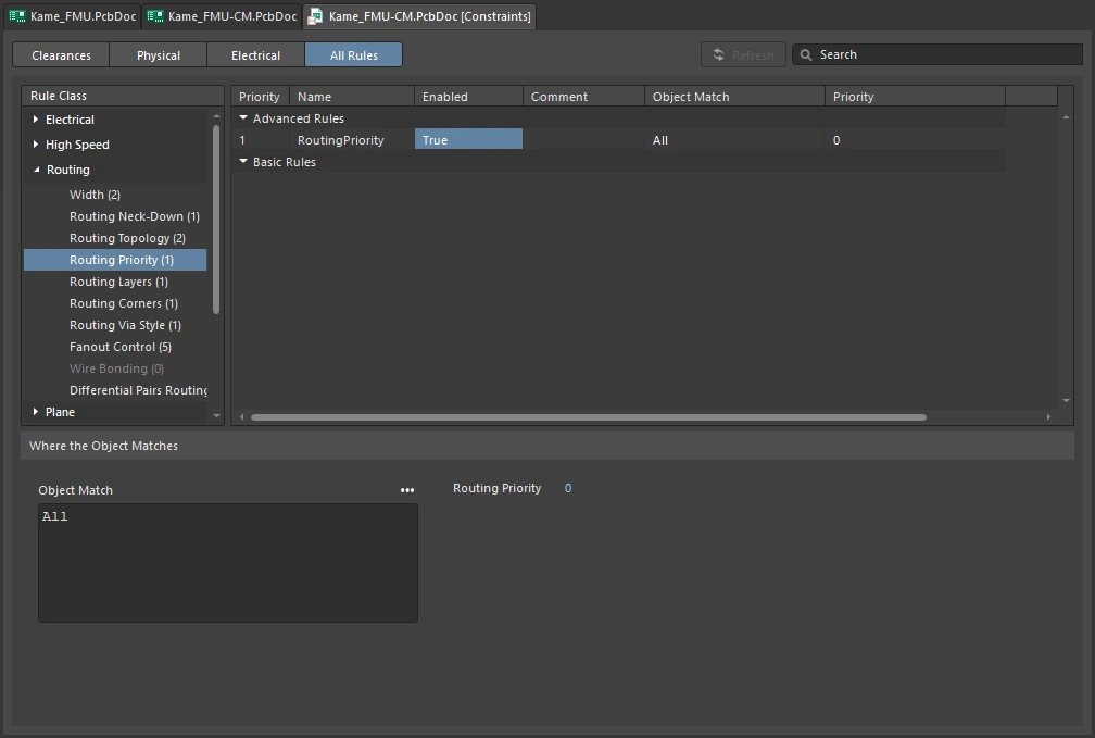
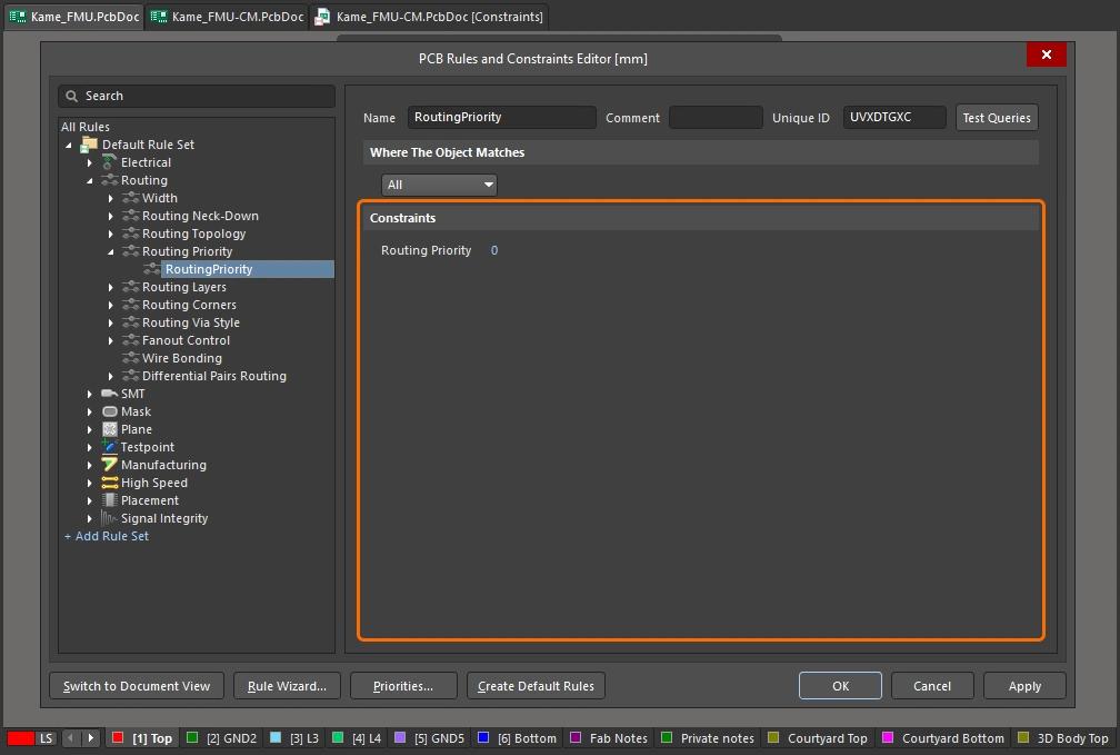
Routing Priority Settings
| Default Rule | Required |
| Routing Priority | The priority value is assigned to the net(s) targeted by the scope (full query) of the rule. Enter a value between 0 and 100. The higher the number assigned, the greater the priority during autorouting. |
| Rule Application | During autorouting. |
Routing Layers
This constraint specifies which layers are allowed to be used for routing.
Constraints
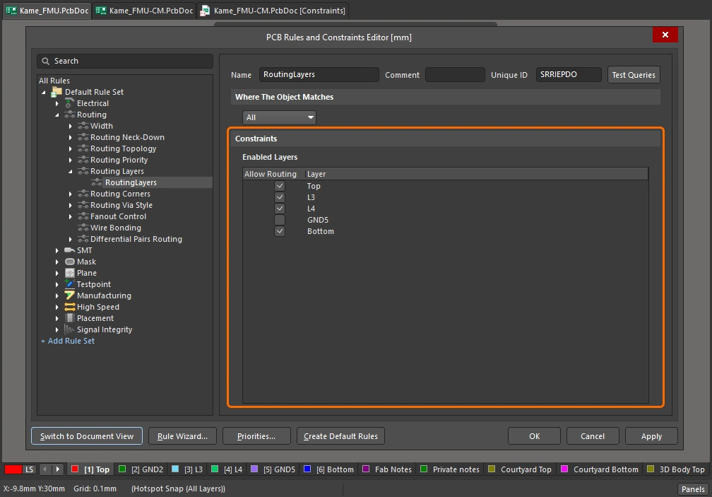
Routing Layers Settings
| Default Rule | Required |
| Enabled Layers | Each signal layer that is currently defined in the layer stack, is listed. Use the associated Allow Routing option to enable/disable routing on a layer, as required. |
| During autorouting | When using the Autorouter, the routing direction for each enabled signal layer in the design is defined as part of the Situs Autorouter setup. Directions are specified in the Layer Directions dialog, accessed by clicking the Edit Layer Directions button in the Situs Routing Strategies dialog. |
| Rule Application | Online DRC, Batch DRC, during interactive routing, and while autorouting. |
Learn more about layers and the layer stack.
Routing Corners
This constraint specifies the corner style to be used during autorouting. This constraint is intended for use by third-party Autorouters that implement 45° routing as a post process. It is not followed by the Situs Autorouter, which implements 45° routing as a native process.
Constraints
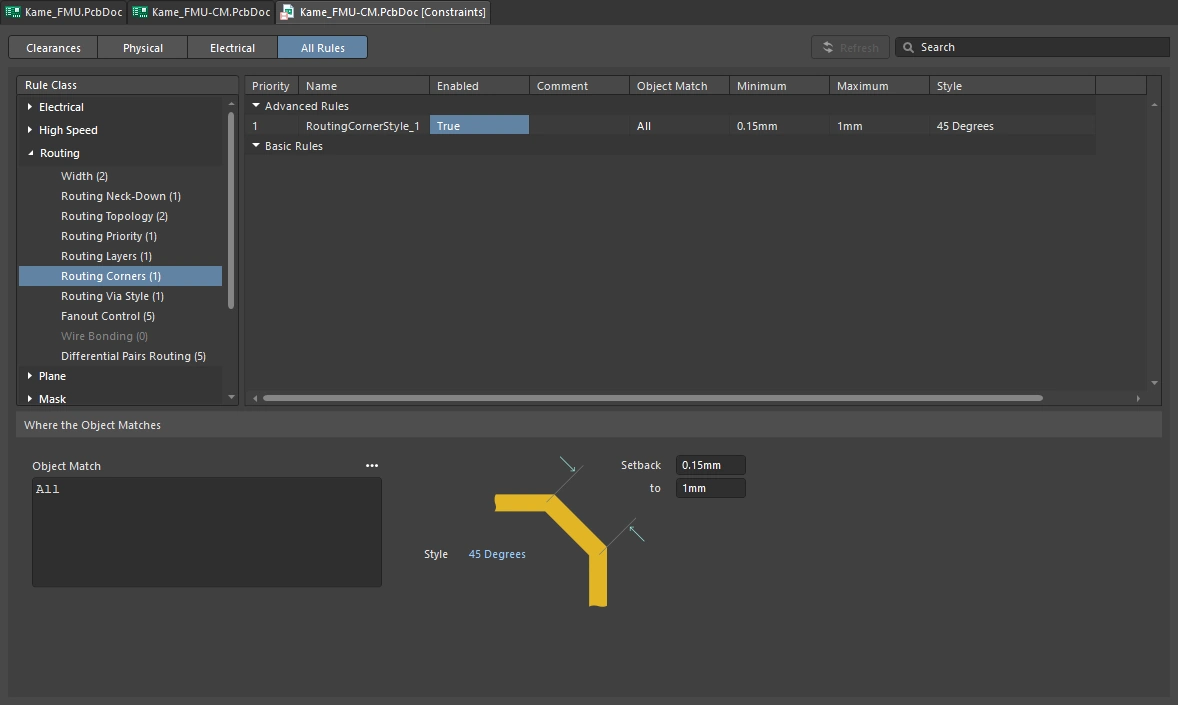
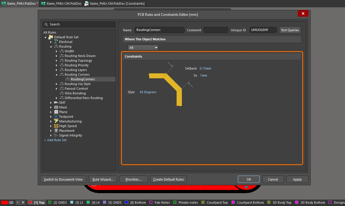
Routing Corner Settings
| Default Rule | Required |
| Style | Specifies which routing corner style to use. The following three styles are available:
|
| Setback | These two fields allow you to define a minimum and maximum value for the setback when using the |
| Rule Application | This constraint is intended for use by third-party Autorouters that implement 45° routing as a post process. It is not followed by the Situs Autorouter, which implements 45° routing as a native process. |
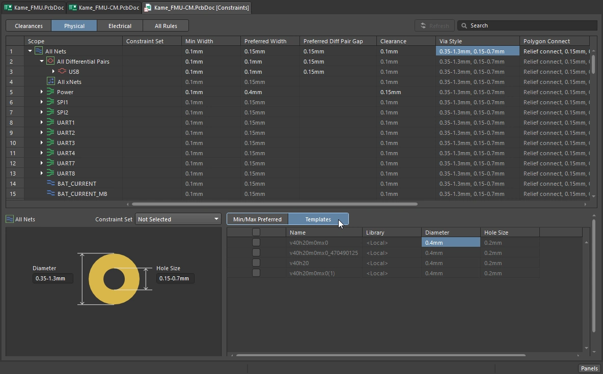
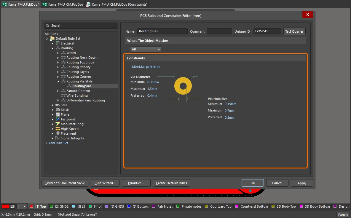
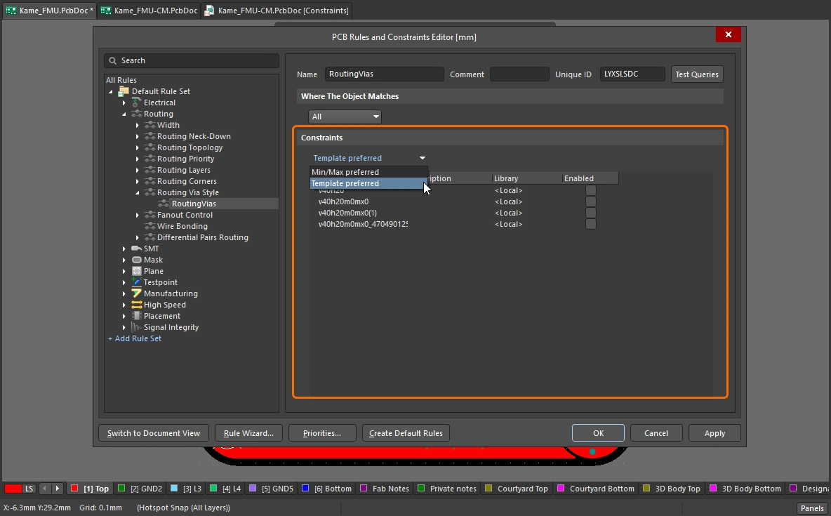
Routing Via Style
This constraint specifies the style of vias that can be used when routing. You can define specific Min/Max/Preferred values for the via's diameter and hole size - defined as part of the rule's constraints - or use templates available to the board design.
Constraints
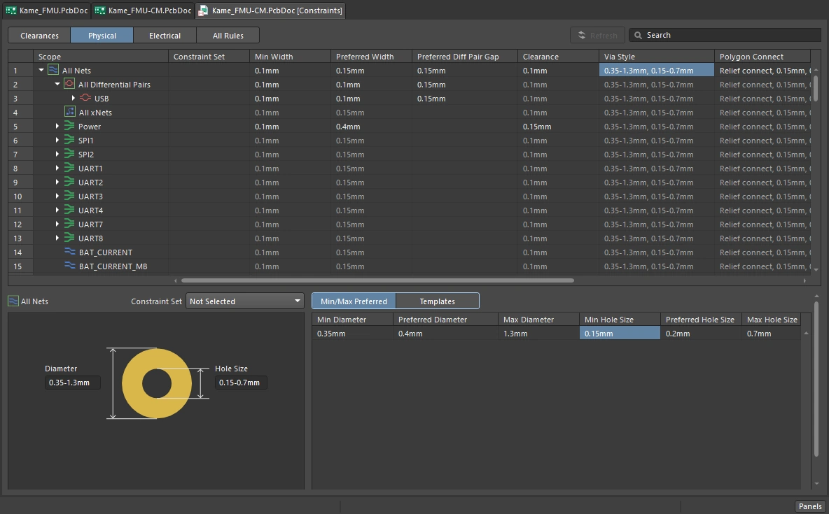
Routing Via Style Settings
| Default Rule | Required |
| Mode | Use the drop-down to choose from the following two modes:
|
Mode = Min/Max preferred (constraint settings) |
Via Diameter - specifies the Minimum, Preferred and Maximum values of the diameter of vias placed during routing. Via Hole Size - specifies the Minimum, Preferred and Maximum values of the hole sizes of vias placed during routing. |
Mode = Min/Max preferred (changing the via size during routing) |
The Routing Via Style design rule defines the X-Y properties of the via. When a via is being placed during interactive routing, you can cycle through the Minimum / Preferred / Maximum / User Choice via definitions by pressing the |
Mode = Template preferred (constraint settings) |
Templates List - lists the available via templates that can be used with the rule. These are via templates (local or defined in Pad Via Template Libraries) that are made available to the board design as part of the Local Pad & Via Library (accessed through the PCB Pad Via Templates panel). For each available template, the following information is presented:
|
Mode = Template preferred (changing the via size during routing) |
When a routing via is about to be placed during interactive routing, you can cycle through the enabled via templates by pressing the 4 key. The selected template is displayed in the Heads-Up Display and on the Status bar. You can also press the Tab key while routing to access the Properties panel, from where you can change the via template currently applied. |
| Changing the via type during routing | The Via Type defines the layers that each via spans in the Z-plane. If there are multiple Via Types defined in the Layer Stack Manager, for example, thruhole and blind/buried vias, it can be possible for different Via Types to be used for the current layer transition. In this situation, press the 6 key to cycle through allowed Via Types. The selected Via Type is displayed in the Heads-Up Display and on the Status bar. Alternatively, press the 8 key to display a pop-up menu of allowed Via Types, and click on the required one (). |
| Controlling the size of blind and buried vias | In order to control the size of blind and buried vias, individual rules can be set up targeting the different layer pairs. For example, to control the via size for blind vias between the top layer and mid-layer 1, the following scope (Full Query) can be used:
To control the via size for buried vias between mid-layer 2 and mid-layer 3, the following scope would be used:
Alternatively, instead of creating individual rules, you can expand the one rule query using ORs as follows:
|
| Rule Application | Online DRC, Batch DRC, during autorouting, and during interactive routing. When the mode of the rule is set to Min/Max preferred, the following considerations apply:
|
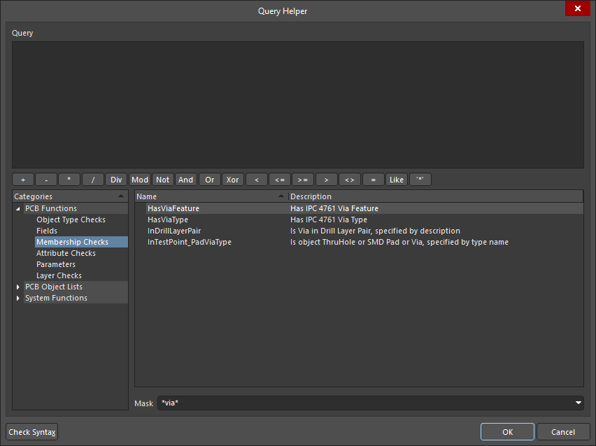
Via Style Query Keywords
There are a large number of via-related query keywords available. The easiest way to browse them is to open the Query Helper dialog and use the mask field to filter all via-related query keywords, as shown in the images below.
-
Attribute Checks via-related query keywords (
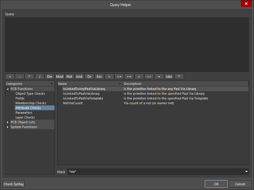 ).
).
-
Field via-related query keywords (
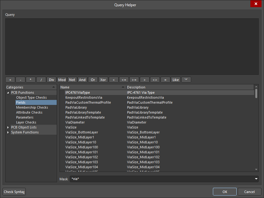 ).
).
-
Membership Checks via-related query keywords (
 ).
).
-
Object Type Checks via-related query keywords (
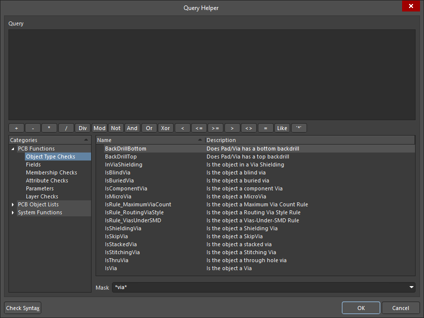 ).
).
Learn more about working with pads and vias.
Learn more about changing via during routing.
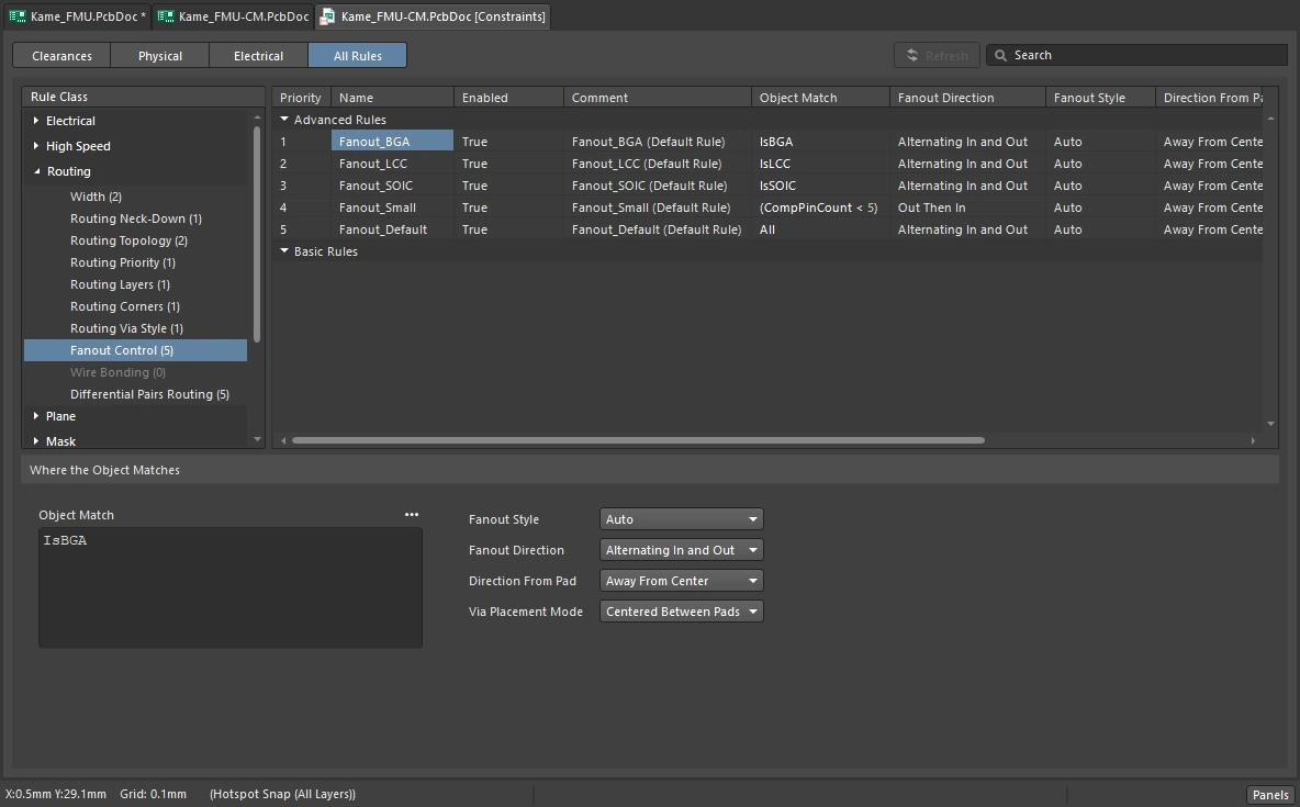
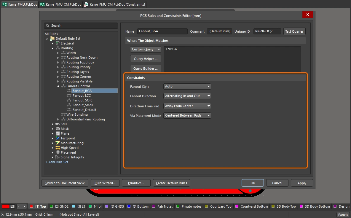
Fanout Control
This constraint specifies fanout options to be used when fanning out the pads of surface mount components in the design that connect to signal and/or power plane nets. From a routing point of view, by adding a via and connecting track a fanout essentially turns an SMT pad into a thru-hole pad. This greatly increases the probability of successfully routing the board, as a signal is made available to all routing layers instead of just the top or bottom layer. This is particularly needed in high-density designs where routing space is very tight.
Constraints
Fanout Control Settings
| Default Rule | Required |
| Fanout Style | Specifies how the fanout vias are placed in relation to the SMT component. The following options are available:
|
| Fanout Direction | Specifies the direction to use for the fanout. The following options are available:
|
| Direction From Pad | Specifies the direction to use for the fanout. When a BGA component is fanned out, its pads are sectioned into quadrants, with fanout applied to the pads in each quadrant simultaneously. The following options are available:
|
| Via Placement Mode | Specifies how the fanout vias are placed in relation to the pads of the BGA component. The following options are available:
|
| Default fanout constraints | The following default Fanout Control design rules are automatically created, covering the typical component package types available (listed in descending order of priority). These rules can be edited or others can be defined in accordance with your individual design requirements.
|
| Fanout vias | The style used for the fanout vias will follow the applicable Routing Via Style design rule(s). Additional tracks laid down as part of the fanout process from pad to via will follow the applicable Routing Width design rule(s). |
| Fanning out a component | To fanout the pads of a component, ensure there are no polygon pours under this component on any layer. Polygons can be shelved before creating fanouts and restored afterward. |
| Rule Application | During interactive routing and autorouting. |
Fanout Control Query Keywords
To target components based on their footprint, look through the Attribute Checks list of query functions for keywords that targets the package type, such as IsBGA, IsLCC, IsSMSIP, and so on.
Learn more about fanout and escape routing.
Wire Bonding
This constraint defines the permissible distance between adjacent bond wires (Wire To Wire), the Min Wire Length and Max Wire Length, and the Bond Finger Margin, which is the distance/padding between a bond wire and the edge of the bond finger pad to which it is wired.
Constraints
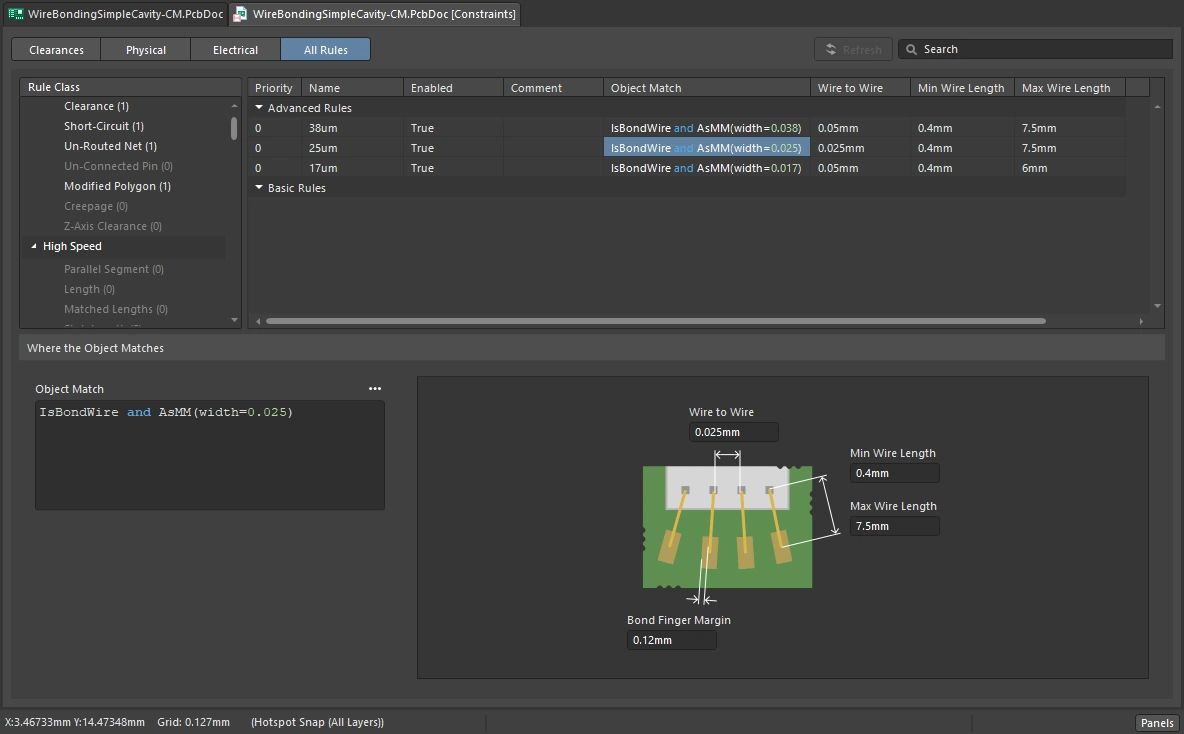
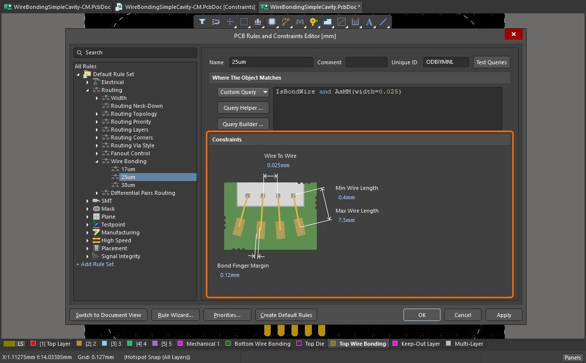
Wire Bonding Settings
| Default Rule | Required |
| Wire To Wire | Specifies the minimum permissible distance between 3D bodies of adjacent bond wires.specifies the minimum permissible distance between 3D bodies of adjacent bond wires. |
| Min Wire Length | Specifies the minimum permissible length of a bond wire. |
| Max Wire Length | Specifies the minimum permissible length of a bond wire. |
| Bond Finger Margin | Specifies the minimum permissible margin from the edge of a bond finger pad. |
| Rule Application | Batch DRC. |
Wire Bonding Query Keywords
-
IsBondFinger – returns an SMD pad primitive on a copper layer that has a bond wire connected to it.
-
IsBondWire – returns a bond wire primitive.
-
IsBondWireConnected – returns any primitive that has a bond wire connected to it.
Learn more about Wire Bonding.
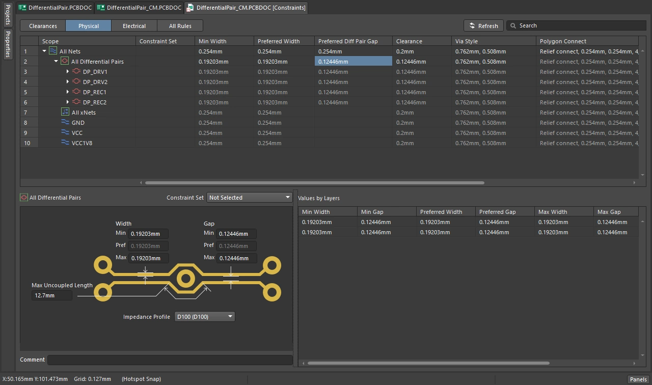
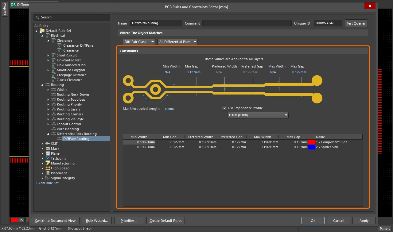
Differential Pairs Routing
This constraint defines the routing width of each net in a differential pair and the clearance (or gap) between the nets in that pair. Differential pairs are typically routed with specific width-gap settings to deliver the required differential impedance needed for that net pair. These settings can be defined manually, or if there are differential pair impedance profiles defined in the Layer Stack Manager, an impedance profile can be selected to automatically define the Preferred width-gap settings.
Constraints
![]()
![]()
Differential Pairs Routing Settings
| Default Rule | Required |
| Min Width | Specifies the minimum permissible width to be used for tracks when routing the differential pair. |
| Min Gap | Specifies the minimum permissible clearance between primitives on different nets within the same differential pair during routing. The Min, Preferred & Max Gap settings in this design rule are used as the differential pair is being routed, rerouted, or interactively modified (during Interactive Sliding). Note that these Gap settings are NOT used during rule checking (DRC). During DRC, the Gap is tested by the applicable Clearance Constraint rule - refer to the Notes below for more information on managing this. |
| Preferred Width | Specifies the preferred width to be used for tracks when routing the differential pair. |
| Preferred Gap | Specifies the preferred clearance between primitives on different nets within the same differential pair. |
| Max Width | Specifies the maximum permissible width to be used for tracks when routing the differential pair. |
| Max Gap | Specifies the maximum permissible clearance between primitives on different nets within the same differential pair. |
| Max Uncoupled Length | Specifies the value for the maximum permissible uncoupled length between positive and negative nets within the differential pair. |
| Use Impedance Profile | This option becomes available when at least one impedance profile is defined in the Layer Stack Manager. When enabled, use the drop-down to select the required impedance profile. When the rule is configured in this mode, the Preferred Width and Preferred Gap required on each routing layer are calculated as part of the specified impedance profile. Once the rule is defined, as you route a differential pair that falls under the scope of the rule, the track widths and pair gap will automatically be set to the values required for that layer to meet the specified impedance. Learn more about Configuring the Layer Stack for Controlled Impedance Routing. |
| Show values for layer stack | This option appears in the dialog when there are multiple layer stacks defined in the Layer Stack Manager. If the board includes multiple layer stacks, then the Differential Pairs Routing Constraints must be configured for each of the layer stacks, using either the all-layer fields above the image, or the layer-specific fields in the Layer Attributes Table, or by selecting an impedance profile. Learn more about Defining and Configuring Substacks. |
| Layer Attributes Table | The grid region at the bottom of the dialog displays all signal layers defined in the layer stack, unless an Impedance Profile is selected. If it is, then only the layers available as part of the selected impedance profile will be displayed. The minimum, maximum and preferred width and gap constraints and other layer-specific information are displayed. The routing Width and Gap fields can be set globally by defining the values in the constraint fields above the image or individually by typing values directly into the table. When an Impedance Profile is selected, the required Preferred width entries are automatically calculated and entered for each layer in the table. In this mode, the Preferred Width and Preferred Gap values cannot be edited, but the Min and Max values can. When defining values for the minimum, maximum and preferred width and/or gap, the Layer Attributes Table will highlight invalid entries using red text. This could happen, for example, when you specify a minimum constraint value that is greater than the maximum constraint value or when setting a preferred constraint value that is lower than the minimum or above the maximum constraint values. The incorrect rule definition is further highlighted by the rule name becoming red in both the folder-tree pane and the respective summary lists in the PCB Rules and Constraints Editor dialog. |
| Differential Pair clearance checking | While the width of each net in a differential pair is monitored by the applicable Differential Pairs Routing rule (and not by a Width rule), clearance checking between the nets in that pair is still governed by the applicable Clearance design rule. If the differential pair routing gap is less than the minimum clearance allowed between different nets on the board, the nets in the differential pairs will fail the clearance constraint. To avoid this, a separate clearance constraint must be created, setting the net-to-net clearance in differential pairs to the same value as the Diff Pair Gap. To do this in the Constraint Manager, set the Clearance value for the pairs to the same value as the Diff Pair Gap. This is demonstrated in the first slide of the Differential Pair Routing slideshow above, where the clearance for the differential pairs has been set to To do this in the PCB Rules and Constraints Editor, add an additional Clearance constraint set to the same clearance value as the Diff Pair Gap, with the Same Differential Pair option selected. This is demonstrated in the fourth slide of the Differential Pair Routing slideshow above, where the clearance for the differential pairs has been set to |
| Changing pair properties across the board | While the optimal Width-Gap settings may be achievable for most of the board, there will often be areas, such as under a BGA component, where smaller and tighter Width-Gap settings must be used. Defining the Min Gap to be less than the Preferred Gap allows the router to bring the pair members closer to each other, where obstacles require this. While this works, it comes at a cost; routing operations become much more complicated and are, therefore, slower. This requirement can also be achieved by defining multiple differential pair routing rules - a lower-priority rule that targets the differential pair across the board and a higher-priority rule that targets the differential pair in the specific area where a narrower Width-Gap setting is required. You then target the differential pair in that area by defining a Room Definition rule for that area and use that room as part of the scope of the differential pair routing rule that requires a tighter Width-Gap setting. |
| Define Differential Pair Classes | To simplify the process of defining the constraints, Differential Pair classes can be defined on the schematic. If the project uses the Constraint Manager this is done in the Constraint Manager (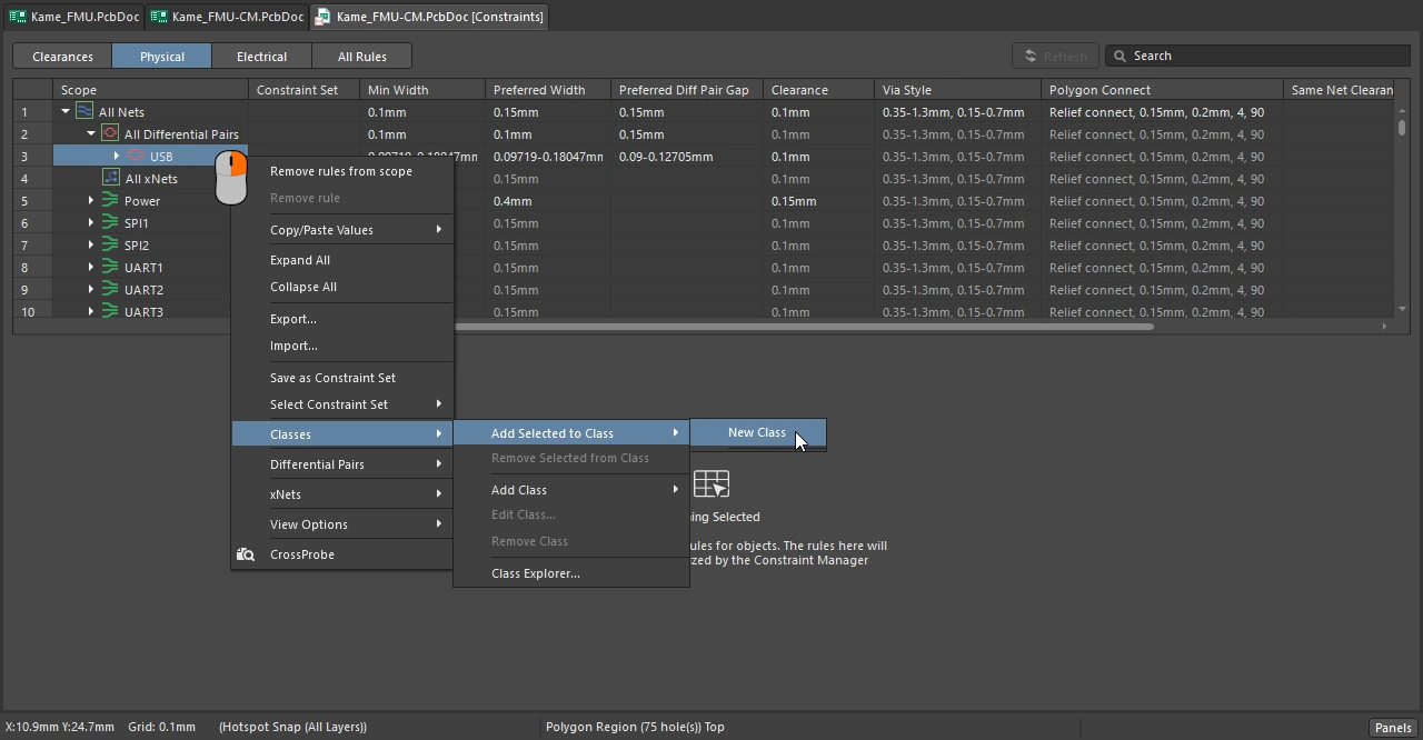 ), if the project uses design rules this is done by adding a Diff Pair Class property to the differential pair directive ( ), if the project uses design rules this is done by adding a Diff Pair Class property to the differential pair directive (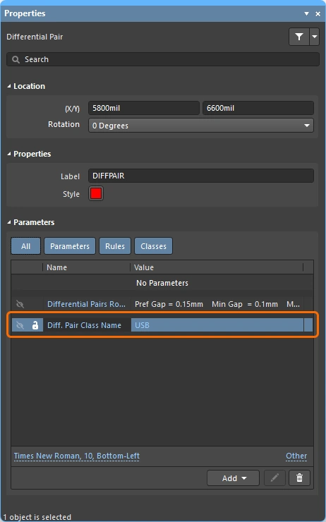 ). ). |
| Rule Application | Online DRC, Batch DRC, interactive routing (and re-routing), autorouting, interactive length tuning (Min Gap is applied), and when interactively modifying the pair, such as sliding a track segment of one of the nets in the pair. |
Differential Pair Routing Query Keywords
-
InAnyDifferentialPair – returns all differential pair objects and their associated primitives.
-
InDifferentialPair – returns all objects associated with differential pair objects whose Name property complies with the Query.
-
InDifferentialPairClass – returns all differential pair objects that are members of the specified Differential Pair Class.
-
IsDifferentialPair – returns all differential pair objects.
-
IsRule_DifferentialPairsRouting – Returns Differential Pairs Routing rule objects.
Learn more about Differential Pair Routing
Learn more about Controlled Impedance Routing