
KB: Prevent unexpected layout, routing, or patterning by configuring design rules with priority
Solution Details
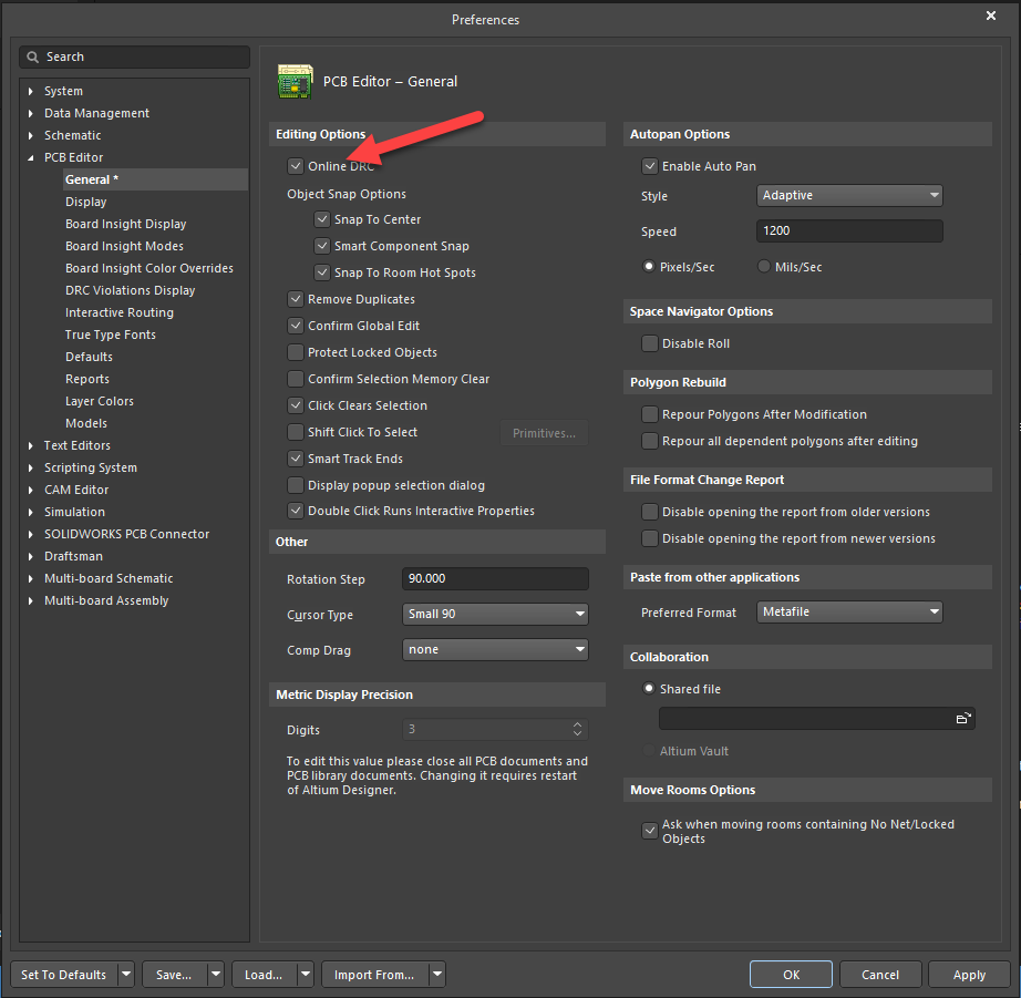
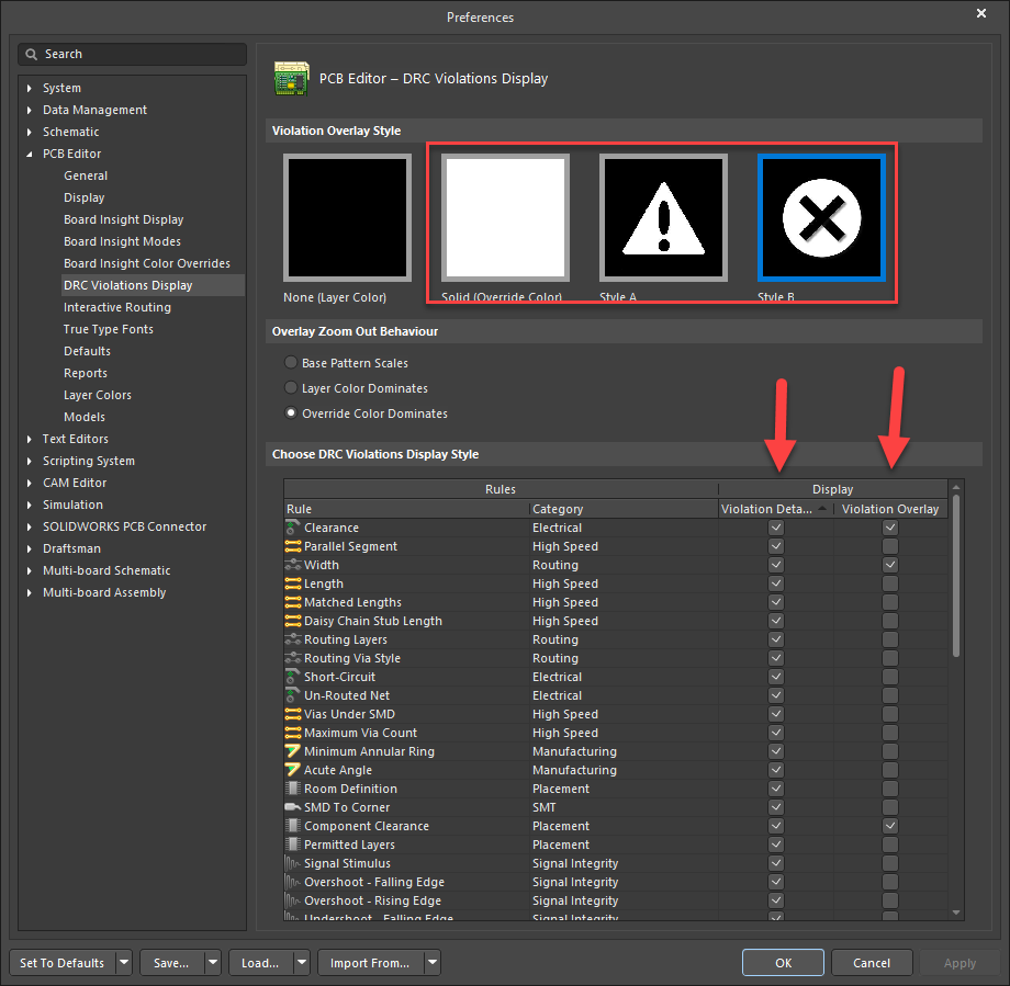
First as a prerequisite, in Preferences, Online DRC is ticked with all violations of interest is ticked to be displayed.
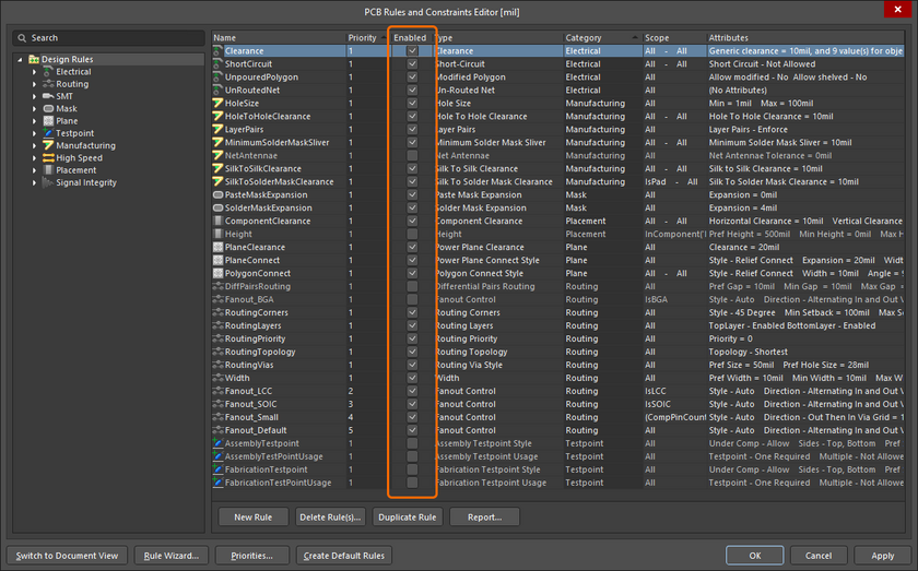
Also, make sure each rule type is to be checked live (online) or in a batch during explicit DRC check from menu Tools » Design Rule Check..., select Rules to Check folder at the top-left, check columns Online and Batch.

Also, ensure all relevant design rules within each rule type are enabled: from menu Design » Rules..., select Design Rules folder in the dialog at the top-left, and check the Enabled column.
With that done, rules of the same kind that have different object scopes need to be ordered correctly in decreasing priority (increasing object scope). Select each rule type and click Priorities button to make sure they are in order of increasing object scope from top to bottom:
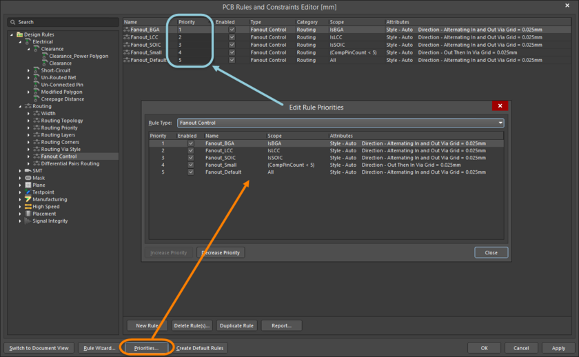
Rule Prioritization
At the lowest priority, most rules are required to have the default catch-all rule (whose object scope set to 'All'). If it is missing or deleted, the resulting PCB layout could be unexpected, as there is no rule governing an arbitrary primitive which is not scoped in any of other higher-priority rules.
Here is a list of rules that require the default catch-all rule and possible consequences (non-exhaustive) if it is missing or misconfigured:
- Clearance » no spacing between copper primitives not scoped
- Short-Circuit
- Un-Routed Net
- Modified Polygon
- Width
- Routing Topology
- Routing Priority
- Routing Layers
- Routing Corners
- Routing Via Style » Vias placed during routing can be of unexpected size/stack
- Fanout Control
- Differential Pairs Routing
- Solder Mask Expansion
- Paste Mask Expansion
- Power Plane Connect Style » no connection to plane layers for vias not scoped
- Power Plane Clearance
- Polygon Connect Style » unknown void/gap in polygon around pads and vias not scoped
- Fabrication and Assembly Testpoint Style » Testpoint Manager fails to assign testpoints on all nets and violation flagged on Fabrication and Assembly Testpoint Usage
- Fabrication and Assembly Testpoint Usage
- Hole Size
- Layer Pairs
- Hole to Hole Clearance
- Minimum Solder Mask Sliver
- Silk to Solder Mask Clearance
- Silk to Silk Clearance
- Net Antennae
- Component Clearance
- Height