
Ansys CoDesigner
Из-за сложности современных электронных изделий, содержащих высокоскоростные и ВЧ‑цепи, в процессе проектирования печатной платы требуется интенсивное взаимодействие между инженерами по PCB и инженерами по моделированию, и это взаимодействие должно быть максимально понятным и простым для обеих сторон. Недостаточно просто экспортировать проект, изменённый инженером по PCB или оптимизированный инженером по моделированию, и передать его другой стороне — также необходимо сообщить, что именно было изменено, что обычно делается по электронной почте или устно. Такой подход несовершенен, поскольку приходится отслеживать все запросы и вручную сравнивать данные, чтобы принять решение об изменениях в проекте или запустить новый анализ. Эти и другие связанные задачи можно решить с помощью Ansys CoDesigner — интерфейса для передачи проектов печатных плат между средами проектирования PCB и моделирования.
Поддерживаемое ПО
В настоящее время поддерживается следующая платформа моделирования и её версии:
Ansys Electronics Desktop (AEDT) — версии 2023 R1, 2023 R2, 2024 R1, 2024 R2
Установка и настройка
Чтобы получить доступ к Ansys CoDesigner в Altium Designer, необходимо установить программное расширение Ansys CoDesigner . Это расширение можно установить или удалить вручную.
Дополнительные сведения об управлении расширениями см. на странице Extending Your Installation (Altium Designer Develop, Altium Designer Agile, Altium Designer).
Чтобы получить доступ к Ansys CoDesigner в Ansys Electronics Desktop, необходимо установить расширение Altium Link. Процесс следующий:
-
Скачайте и распакуйте архив расширения Altium Link. Его можно получить, связавшись с ansyscollaboration@altium.com (укажите используемую версию AEDT).
-
Убедитесь, что приложение AEDT закрыто.
-
В распакованной папке найдите файл
install_altiumlink.bat, щёлкните по нему правой кнопкой мыши и выберите Run as administrator. -
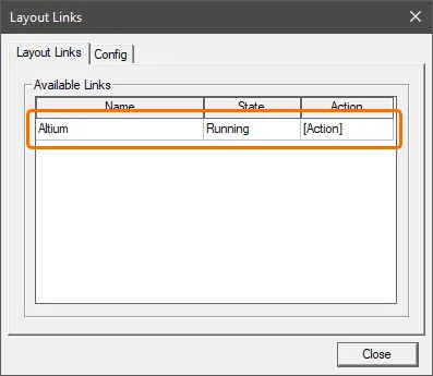
Откройте AEDT и выберите команду Tools » Layout Links в главном меню.
-
На вкладке Config в открывшемся диалоговом окне Layout Links нажмите кнопку Add Link, перейдите в папку
\AnsysEM\<version>\Win64с программными файлами AEDT и откройте файлaltiumlink.dll. -
На вкладке Layout Links диалогового окна Layout Links убедитесь, что ссылка Altium присутствует в списке, и закройте диалог.
Как это работает
После добавления функциональности Ansys CoDesigner в ПО для проектирования PCB и моделирования она может передавать изменения проекта в обе стороны. Изменения проекта передаются через Altium 365 Workspace, который служит мостом между двумя доменами. Преимущество передачи изменений через Workspace в том, что процесс обновления становится stateless. Это означает, что каждая сторона может продолжать работу независимо; не нужно беспокоиться о том, на каком этапе процесса проектирования/моделирования находится другая команда.
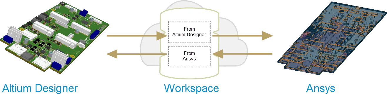
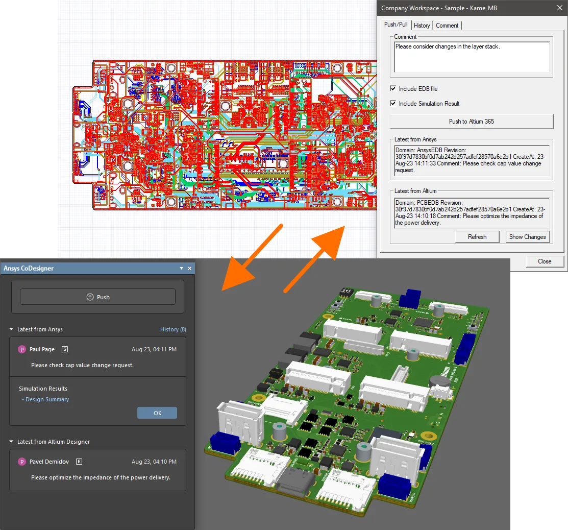
Ansys CoDesigner обеспечивает двунаправленный push/pull изменений проекта между двумя доменами. В Altium Designer обнаруживаются изменения стека слоёв и материалов, компонентов и примитивов, и они могут быть применены в AEDT. В AEDT предлагаемые изменения стека слоёв и материалов могут быть отправлены через файл EDB и обнаружены/применены в Altium Designer. Инженеры ECAD и инженеры по моделированию могут общаться с помощью системы комментариев, при этом каждая ветка комментариев привязана к конкретному компоненту в проекте. Результаты моделирования могут быть отправлены из AEDT в Altium 365 Workspace и связаны с ревизией проекта, с возможностью просмотра через браузерный интерфейс Workspace и предварительного просмотра в Altium Designer.
Интерфейс совместной работы
-
В Altium Designer панель Ansys CoDesigner используется для отправки (Push) и получения (Pull) изменений проекта в обе стороны и отображения сообщений.
Панель Ansys CoDesigner открывается из редактора PCB в Altium Designer нажатием кнопки Panels в правом нижнем углу рабочей области и выбором пункта Ansys CoDesigner в появившемся меню. Обратите внимание: для доступа к панели необходимо быть подключённым к Workspace, а документ PCB должен входить в проект PCB, сохранённый в этом Workspace, чтобы вы могли использовать данную функциональность.
-
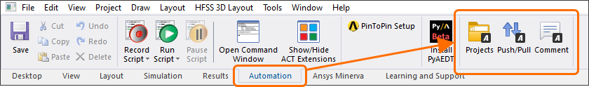
В AEDT диалоги, доступные из диалогового окна Layout Links (Tools » Layout Links) или с вкладки Desktop ленты при открытом проекте, используются для:
- Подключения к вашему Altium 365 Workspace и импорта из него проекта PCB.
- Отправки (Push) проекта в Workspace и получения (Pull) его из Workspace.
- Просмотра истории обмена данными между Altium Designer и AEDT.
- Добавления комментариев к компонентам в проекте.
Отправка изменений из Altium Designer
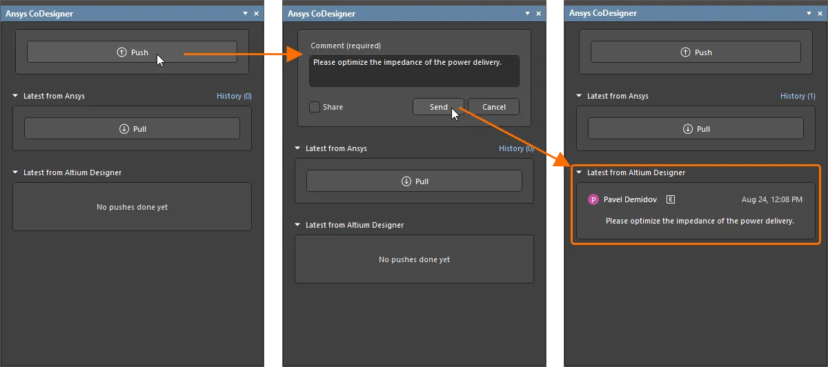
Чтобы отправить проект из Altium Designer, нажмите кнопку Push на панели Ansys CoDesigner . В верхней части панели появится окно редактирования. Введите сообщение об изменении проекта, затем нажмите Send. Область Latest from Altium Designer панели Ansys CoDesigner будет обновлена и отобразит сведения об этой отправке.
Затем проект можно импортировать в AEDT. Для проекта, который уже был импортирован, изменения можно получить в AEDT.
Push and Share для приглашения инженера по моделированию
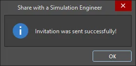
Когда вы нажимаете Push на панели Ansys CoDesigner , вы также можете включить параметр Share ниже поля Comment , чтобы отправить инженеру по моделированию приглашение по электронной почте с помощью диалогового окна Share with a Simulation Engineer, которое откроется после нажатия кнопки Send.
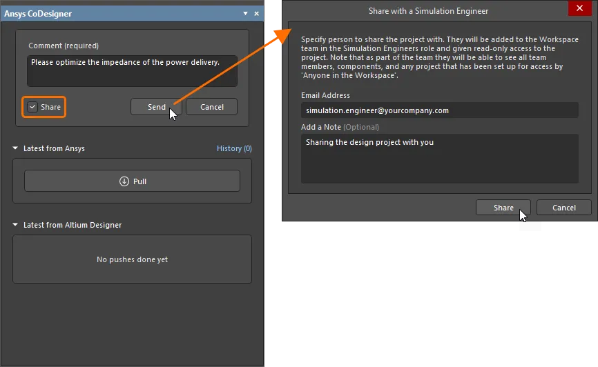
Введите адрес электронной почты инженера по моделированию и необязательное примечание (при необходимости), затем нажмите кнопку Share . Вы можете поделиться с человеком, который уже является участником команды вашего Workspace, с другим зарегистрированным пользователем Altium внутри или вне вашей организации, либо с пользователем, у которого нет учётной записи Altium. Может появиться диалог уведомления, предупреждающий, что пользователь с указанным email может быть вне вашей организации — нажмите OK , чтобы всё равно пригласить его.
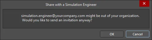
Через небольшую паузу появится ещё одно диалоговое окно, подтверждающее, что приглашение было успешно отправлено.
В рамках процесса приглашения:
- Пользователю, который уже является участником команды вашего Workspace, проект будет предоставлен в общий доступ с правами просмотра (View), и он получит письмо‑приглашение, с помощью которого сможет получить доступ к проекту в Workspace.
- Пользователь, который не является участником команды вашего Workspace, но имеет учётную запись Altium (независимо от того, находится ли он внутри или вне вашей организации), будет добавлен в команду Workspace, и проект будет предоставлен ему в общий доступ с правами просмотра (View). Он получит письмо‑приглашение, с помощью которого сможет получить доступ к проекту в Workspace.
- Пользователь без учётной записи Altium получит письмо, направляющее его на промежуточную форму для регистрации/создания учётной записи Altium. После регистрации он будет добавлен в команду Workspace, и проект будет предоставлен ему в общий доступ с правами просмотра (View).
Получение изменений в Altium Designer
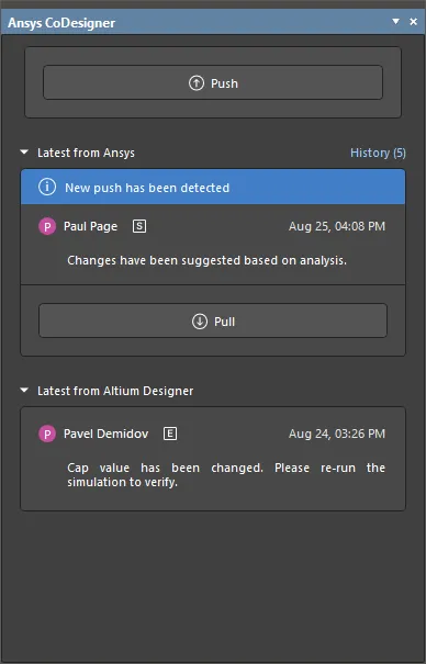
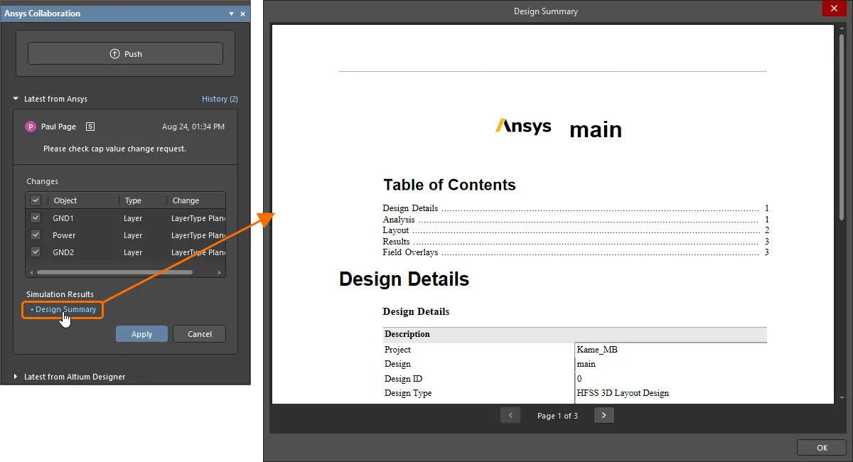
Когда новые изменения отправляются из AEDT, на панели Ansys CoDesigner автоматически появляется баннер New changes have been detected . На панели будут указаны имя инженера по моделированию, выполнившего Push, и необязательный комментарий, который он ввёл при отправке.
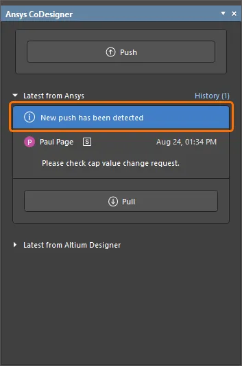
Когда нажимается кнопка Pull и если файл EDB был включён в Push из AEDT, в списке отображаются все изменения, которые необходимо внести в рабочий файл, чтобы синхронизировать его со снимком (snapshot) в вашем Workspace. Каждое обнаруженное различие перечисляется в списке Changes на панели. Снимите флажок для каждого изменения, которое вы не хотите применять. Когда будете готовы, нажмите кнопку Apply , чтобы применить все включённые изменения к проекту.
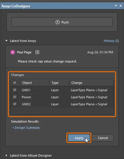
Если результаты моделирования были включены в Push из AEDT, на панели будет показан элемент управления Design Summary . Нажмите этот элемент управления, чтобы открыть результаты моделирования в диалоге Design Summary.
Импорт проекта в AEDT
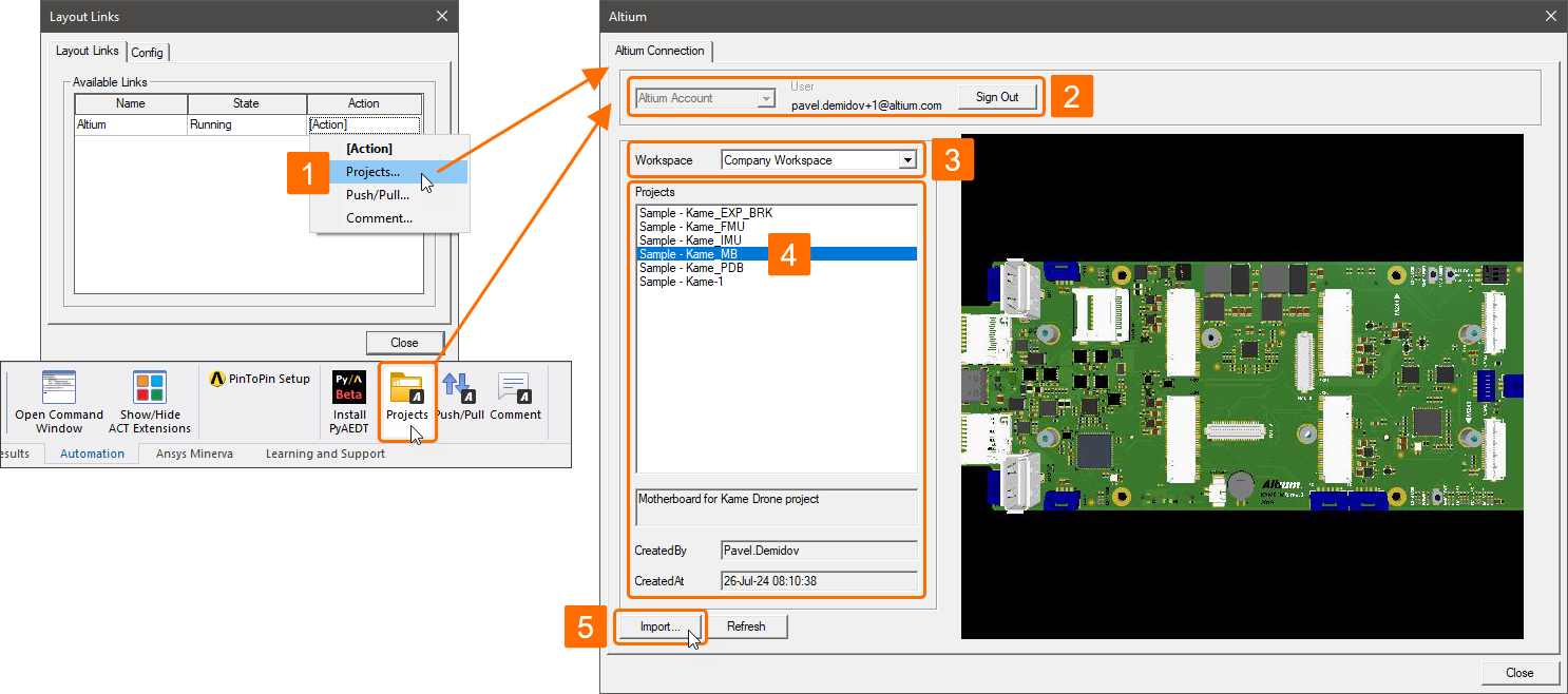
Чтобы начать работу с проектом PCB в AEDT, его сначала необходимо импортировать в AEDT. Для этого:
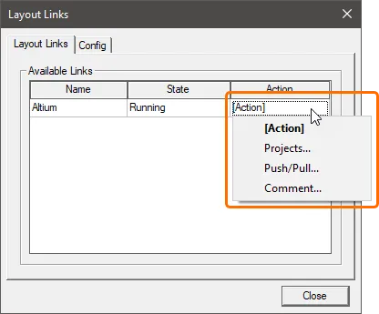
- В диалоге Layout Links (Tools » Layout Links) щёлкните ячейку [Action] для ссылки Altium на вкладке Layout Links и выберите Projects. Либо нажмите кнопку Projects на вкладке Desktop ленты, когда проект открыт. Откроется диалог Altium.
-
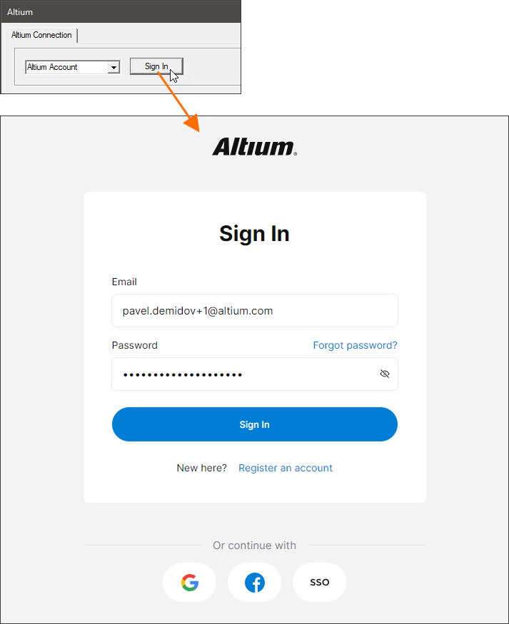
Войдите в свою учётную запись Altium. Убедитесь, что в раскрывающемся списке в верхней части диалога выбран пункт Altium Account, и нажмите кнопку Sign In. В браузере по умолчанию откроется страница, где можно ввести учётные данные Altium или использовать SSO для входа в учётную запись Altium — show example.
- Выберите Workspace, в котором находится нужный проект, из раскрывающегося списка Workspace.
-
Выберите проект в списке Projects и нажмите кнопку Import.
- Сохраните файл проекта AEDT с помощью открывшегося диалога Save As, затем закройте диалог Altium.
Отправка изменений из AEDT
Чтобы выполнить push проекта из AEDT:
- В диалоге Layout Links (Tools » Layout Links) щёлкните ячейку [Action] для ссылки Altium на вкладке Layout Links и выберите Push/Pull. Либо нажмите кнопку Push/Pull на вкладке Desktop ленты, когда проект открыт.
- Используйте поле Comment в верхней части открывшегося диалога, чтобы добавить комментарий с описанием того, что включено в Push.
- Включите параметры Include EDB file (чтобы отправить изменения проекта) и/или Include the Simulation Result (чтобы отправить результаты моделирования).
- Нажмите кнопку Push to Altium 365. Область Latest from Ansys диалога будет обновлена сведениями об этой отправке.
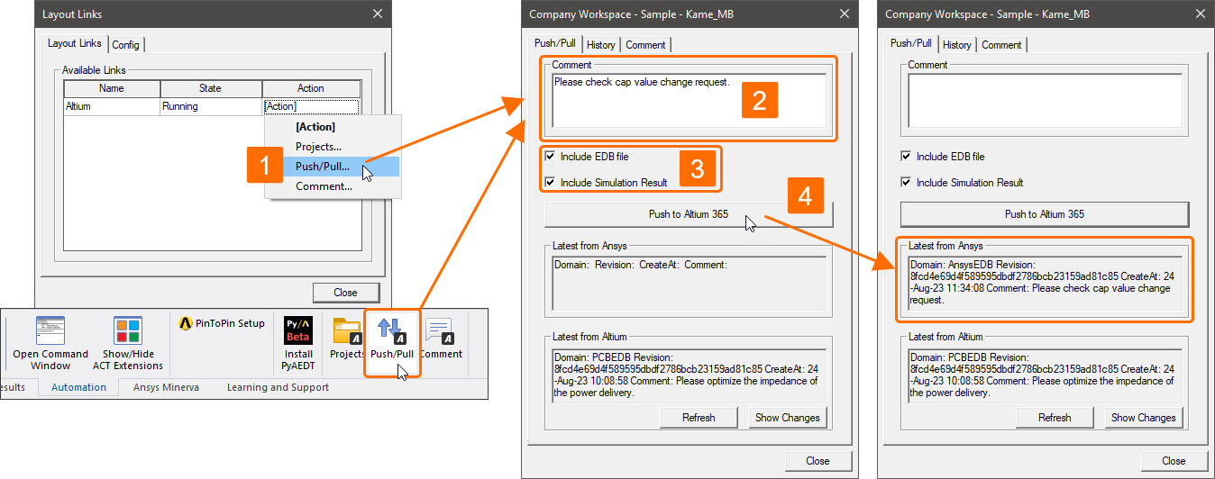
Push будет обнаружен в Altium Designer, и его можно будет подтянуть (pull) в Altium Designer как описано выше.
Получение изменений в AEDT
Когда изменения проекта были pushed from Altium Designer, их можно подтянуть (pull) в AEDT.
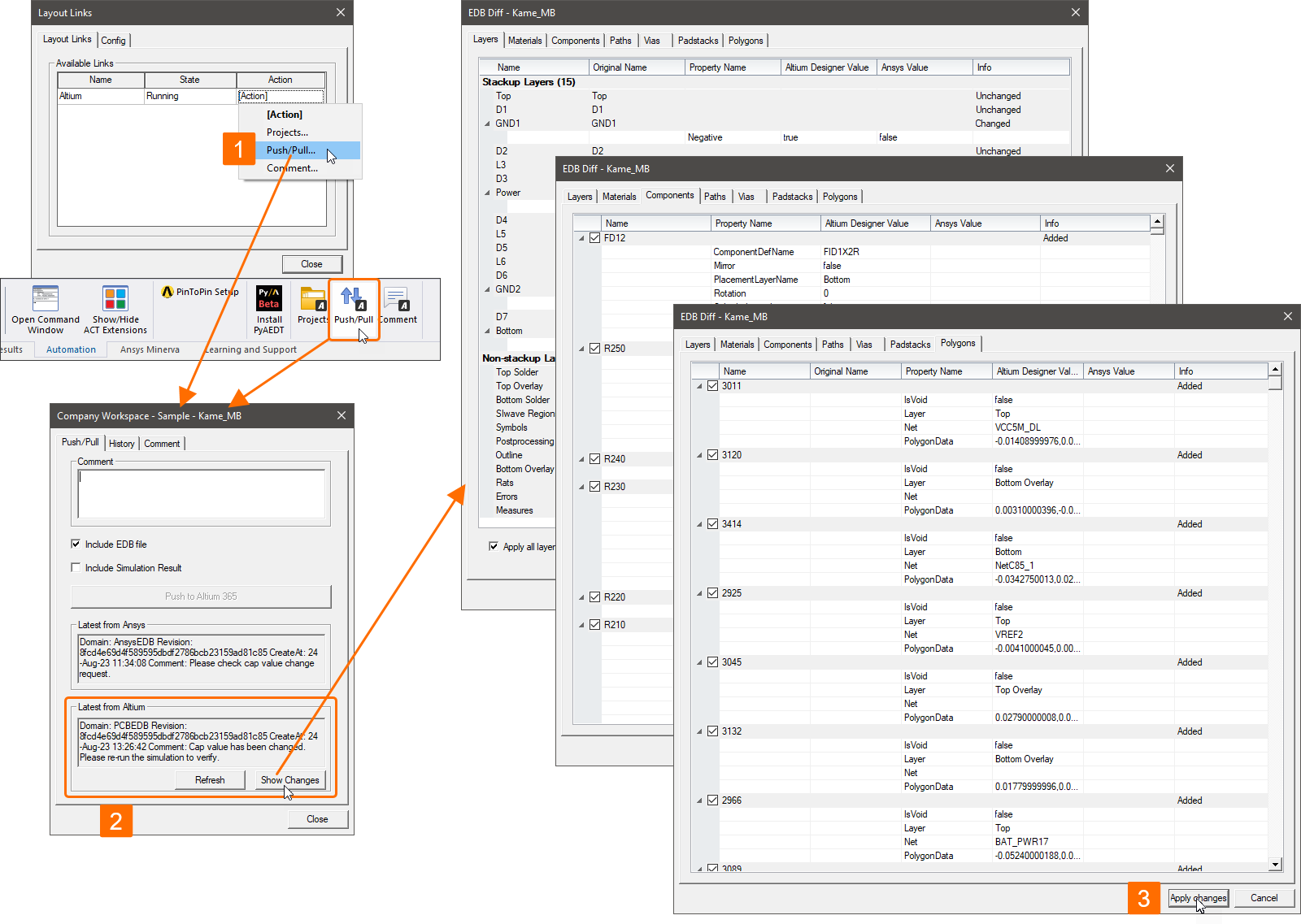
- В диалоге Layout Links (Tools » Layout Links) щёлкните ячейку [Action] для ссылки Altium на вкладке Layout Links и выберите Push/Pull. Либо нажмите кнопку Push/Pull на вкладке Desktop ленты, когда проект открыт.
-
Проверьте область Latest From Altium открывшегося диалога — там содержится информация о последнем push из Altium Designer — и нажмите кнопку Show Changes, чтобы открыть диалог, в котором описаны различия между проектом в Workspace и текущим проектом в AEDT. Используйте флажки на вкладках диалога, чтобы выбрать изменения, которые вы хотите применить к проекту в AEDT.
- После просмотра изменений нажмите кнопку Apply changes, чтобы применить изменения к проекту в AEDT.
Просмотр истории обмена
История push и pull проекта сохраняется.
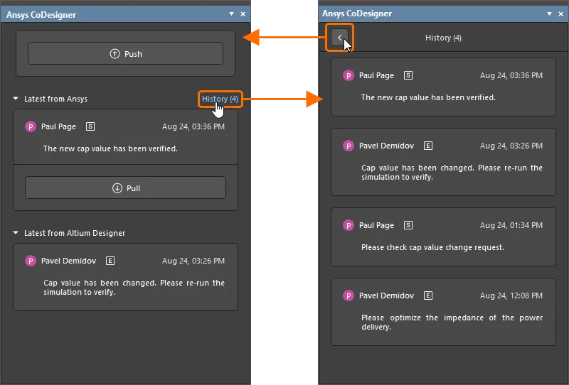
Чтобы просмотреть историю в Altium Designer, нажмите элемент управления History справа от заголовка области Latest from the Ansys на панели Ansys Codesigner . Откроется список push и pull как из Altium Designer, так и из Ansys. Используйте кнопку ![]() в верхней части панели, чтобы вернуться к последним изменениям.
в верхней части панели, чтобы вернуться к последним изменениям.
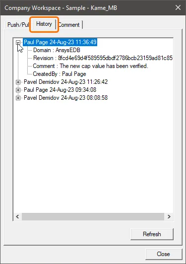
Чтобы просмотреть историю в AEDT, щёлкните ячейку [Action] для ссылки Altium на вкладке Layout Links диалога Layout Links (Tools » Layout Links) и выберите Push/Pull или Comment либо нажмите кнопку Push/Pull или Comment на вкладке Desktop ленты. Выберите вкладку History в открывшемся диалоге. Разверните запись push/pull, чтобы увидеть её детали. Используйте кнопку Refresh, чтобы обновить вкладку последними данными.
Добавление комментариев в Altium Designer и AEDT
И инженеры-электронщики, и инженеры по моделированию также могут воспользоваться поддержкой комментариев в Workspace, создавая ветки комментариев, привязанные к конкретным компонентам.
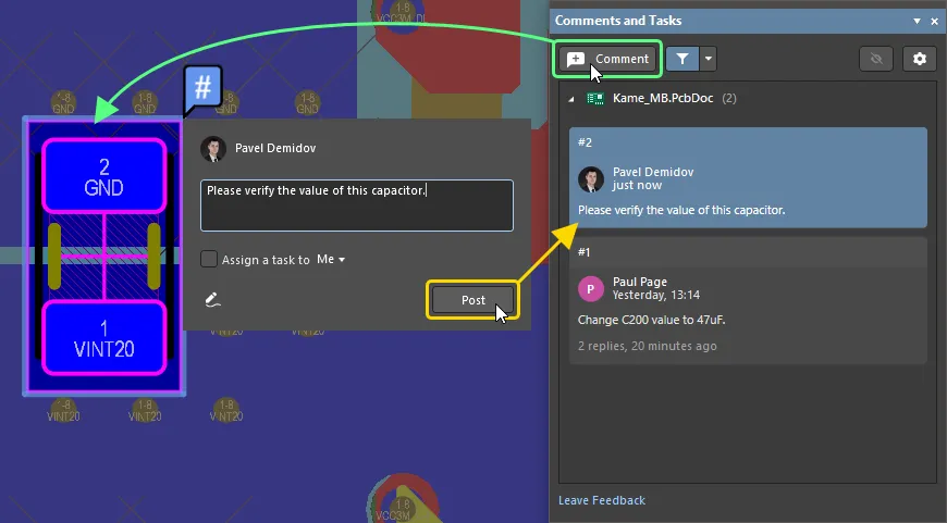
В Altium Designer существующие комментарии доступны через панель Comments and Tasks.
-
Чтобы добавить новый комментарий к компоненту на PCB, нажмите кнопку Comments в верхней части панели, наведите курсор на компонент в рабочей области, чтобы он подсветился синей рамкой, и щёлкните. В открывшемся диалоге ввода комментария введите комментарий и нажмите Post.
-
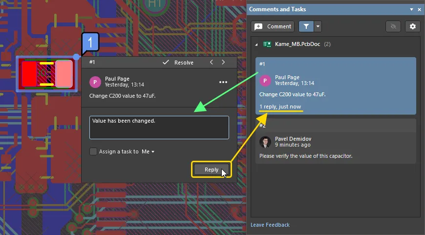
Чтобы ответить на комментарий, выберите запись комментария на панели Comments and Tasks, введите ответ в предоставленное текстовое поле в диалоге ввода комментария и нажмите Reply. Ответ будет добавлен в ветку комментариев.
Подробнее см. на странице Document Commenting.
В AEDT ветки комментариев управляются через вкладку Comments диалога Altium, доступного по щелчку ячейки [Action] для ссылки Altium на вкладке Layout Links диалога Layout Links (Tools » Layout Links) и выбору Comment. Список в верхней части диалога показывает существующие ветки комментариев для проекта.
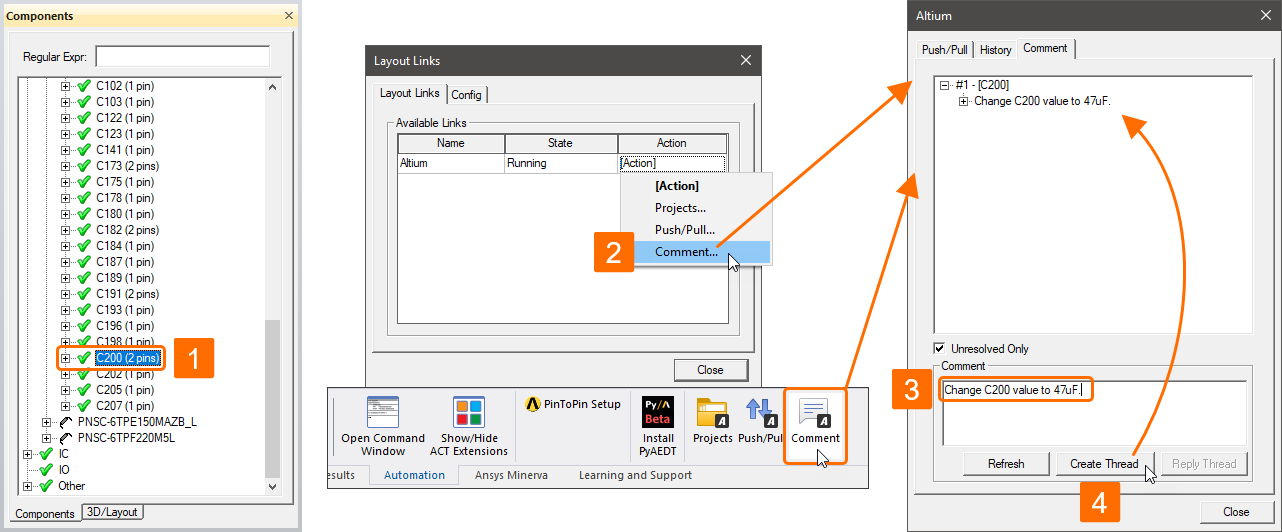
Чтобы добавить комментарий к компоненту в AEDT:
- Выберите конкретный компонент на панели Components (View » Components) или в рабочей области проекта.
- В диалоге Layout Links (Tools » Layout Links) щёлкните ячейку [Action] для ссылки Altium на вкладке Layout Links и выберите Comment.
- Введите комментарий в поле Comment в нижней части открывшегося диалога.
- Нажмите кнопку Create Thread . Новая ветка будет добавлена в список.
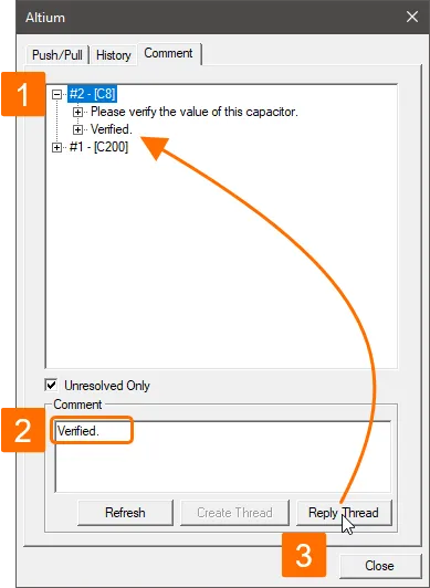
Чтобы ответить на существующую ветку из AEDT:
- Выберите пронумерованную запись комментария в списке на вкладке Comments диалога Altium.
- Введите ответ в поле Comment в нижней части диалога.
- Нажмите кнопку Reply Thread . Новый ответ будет добавлен под записью соответствующей ветки комментариев в списке.
 Локализовано с помощью ИИ