
Новое в Altium Designer
На этой странице описаны улучшения, включенные в выпуски Altium Designer, Altium Designer Develop и Altium Designer Agile. Наряду с широким спектром улучшений, развивающих и совершенствующих существующие технологии, каждое обновление также включает ряд исправлений и доработок по всему программному обеспечению на основе отзывов, оставленных клиентами через систему BugCrunch сообщества AltiumLive, помогая вам и дальше создавать передовые электронные устройства.
Версия 26.8
Altium Designer Develop – Released: 9 July 2026 – Version 26.8.1 (build 9)
Altium Designer Agile – Released: 9 July 2026 – Version 26.8.1 (build 50)
Altium Designer – Released: 9 July 2026 – Version 26.8.1 (build 31)
Примечания к выпуску Altium Designer
Улучшение проектирования печатных плат
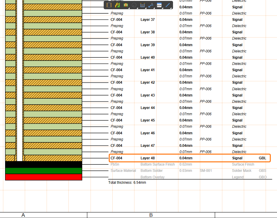
Увеличено количество сигнальных слоев (Open Beta)
В этом выпуске количество сигнальных слоев, которые могут присутствовать в проекте PCB, было увеличено с 32 до 128. Такая возможность часто необходима для более крупных и сложных проектов и особенно хорошо подходит именно для них.
Как и следовало ожидать, все части программного обеспечения, затронутые расширенной поддержкой слоев, и в особенности редактор PCB, были обновлены для ее поддержки, включая Layer Stack Manager, View Configuration panel, Properties panel, фильтрацию, DRC, генерацию выходных данных и так далее. Некоторые примеры затронутых областей показаны ниже в слайд-шоу.
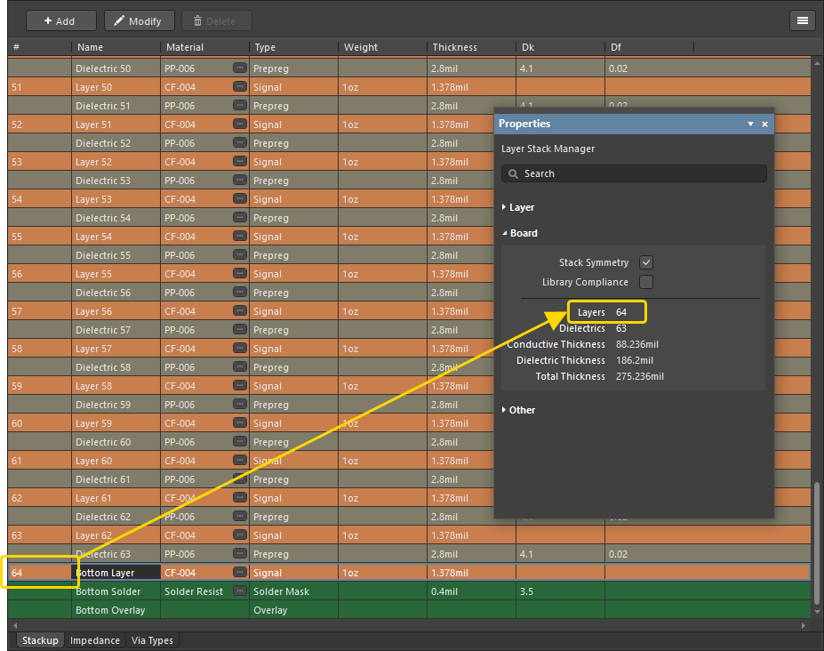
Дополнительную информацию см. на странице Определение стека слоев.
Улучшение Constraint Manager
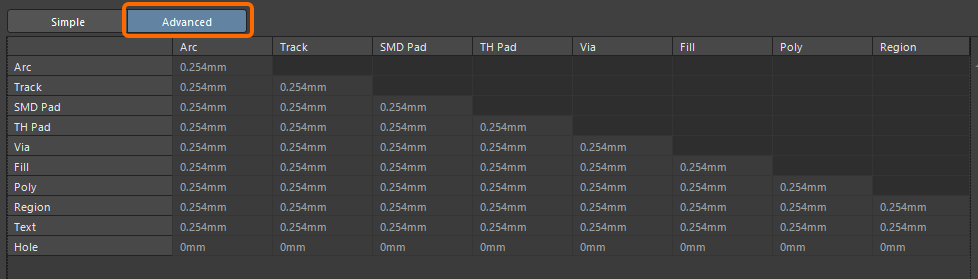
Расширенное управление режимами правила зазора
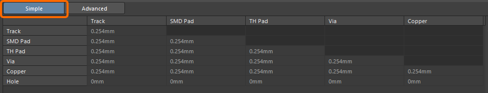
При создании расширенного правила Clearance из представления All Rules при доступе к Constraint Manager из PCB были добавлены новые элементы управления, позволяющие переключаться между режимами работы матрицы минимальных зазоров «Simple» и «Advanced» (аналогично диалогу PCB Rules and Constraints Manager). В режиме Simple объекты Track и Arc (включая объекты Track Keepout и Arc Keepout) объединяются в единую запись «Track». Объекты Fill, Poly и Region (включая объекты Fill Keepout и Region Keepout) объединяются в единую запись «Copper». Обратите внимание, что запись для объектов «Text» в этом режиме скрыта. В режиме Advanced отображаются все объекты.
Дополнительную информацию о создании расширенного правила см. на странице Определение проектных требований с помощью Constraint Manager.
Улучшение Draftsman
Добавлен курсор «рука» для панорамирования
Теперь при панорамировании производственного чертежа на базе Draftsman (*.PCBDwf, *.HarDwf, *.MbDwf) с помощью функции Right-click, Hold&Drag отображается курсор «рука», что соответствует поведению редакторов схем и PCB.
Дополнительную информацию см. на странице Горячие клавиши для редактора Altium Designer Draftsman.
Улучшение импорта/экспорта
Расширенный движок OrCAD (Open Beta)
В этом выпуске представлен новый расширенный движок OrCAD при импорте ваших проектов и библиотек OrCAD с помощью мастера импорта.
Дополнительную информацию см. на странице Импорт проекта из OrCAD.
Функции, ставшие полностью общедоступными в Altium Designer 26.8
Следующие функции в этом выпуске теперь официально имеют статус Public:
Версия 26.7
Altium Designer Develop – Released: 8 June 2026 – Version 26.7.1 (build 13)
Altium Designer Agile – Released: 8 June 2026 – Version 26.7.1 (build 25)
Altium Designer – Released: 8 June 2026 – Version 26.7.1 (build 11)
Примечания к выпуску Altium Designer
Key Highlights
Улучшение Wire Bonding
Управление видимостью соединительных проводов и контактных площадок кристалла (Open Beta)
При просмотре PCB в режиме 2D Layout Mode теперь можно управлять видимостью соединительных проводов с помощью новой записи Bond Wires (и связанных с ней элементов управления) в области Object Visibility на вкладке View Options панели View Configuration.


При просмотре PCB в режиме 3D Layout Mode видимость соединительных проводов и контактных площадок кристалла теперь управляется в рамках параметра Show 3D Bodies в области General Settings на вкладке View Options панели View Configuration.


Дополнительную информацию о wire bonding см. на странице Wire Bonding.
Улучшение платформы
Возможность перевести author seat в roaming в Altium Designer Develop
Теперь администратор рабочего пространства Altium Develop может зарезервировать author seat за указанным участником Workspace с помощью страницы Admin – Usage and Billing в браузерном интерфейсе Workspace. Это позволяет участнику Workspace работать с Altium Designer Develop (26.7 и новее) в офлайн-режиме, без подключения к Workspace Altium Develop и без входа в свой аккаунт Altium, в течение срока подписки. При этом в любой момент администратор Workspace может отозвать этот roamed seat.
Когда author seat используется в режиме roaming в Altium Designer Develop, рядом с элементом управления Active Server отображается значок ![]() .
.

Дополнительную информацию см. на странице Authoring Access in Altium Designer Develop .
Функции, ставшие полностью общедоступными в Altium Designer 26.7
Следующие функции в этом выпуске теперь официально имеют статус Public:
Версия 26.6
Altium Designer Develop – Released: 19 May 2026 – Version 26.6.0 (build 14)
Altium Designer Agile – Released: 19 May 2026 – Version 26.6.0 (build 21)
Altium Designer – Released: 19 May 2026 – Version 26.6.0 (build 10)
Примечания к выпуску Altium Designer
Key Highlights
Улучшение проектирования печатных плат
Обновленные пакеты IPC Compliant Footprint Wizard
Updated All Packages for Compliance with IPC Standard 7351, Revision B
IPC Compliant Footprint Wizard был обновлен для всех уже поддерживаемых корпусов, чтобы генерация посадочных мест соответствовала редакции B стандарта IPC Standard 7351 - Generic Requirements for Surface Mount Design and Land Pattern Standard. Несколько областей были обновлены для обеспечения совместимости. В их число входят (но не ограничиваются ими):
-
Формулы размеров площадок и зазоров
-
Проблема округления при наложении
-
Сопоставление слоев
-
Шелкография и courtyard
-
Значения таблицы плотности
-
Установка выходного контура корпуса на максимальные значения
Added Ability to Control Pad Trimming for a Gullwing Package Footprint
Страница Footprint Dimensions в Wizard была расширена возможностью управлять тем, применяется ли подрезка площадок при использовании вычисленных значений посадочного места при генерации посадочного места корпуса gullwing (в примере на изображении ниже используется SOT23 ). Используйте раскрывающийся список Trim Pad, чтобы выбрать нужный вариант подрезки.

Additional Updates
-
При определении размеров корпуса MOLDED был добавлен новый параметр Lead Span Range (L) . Это позволяет задавать минимальные и максимальные значения расстояния между внешними сторонами выводов.
-
Параметр Body Length Range (L) был переименован в Body Length Range (L1) , а изображения для корпуса MOLDED были обновлены.

-
При создании корпуса SODFL или MOLDED (polarized) поляризованный вывод (катод) теперь обозначается в сгенерированной 3D STEP-модели только белой полосой (SODFL) либо белой полосой и фаской (MOLDED).
-
При создании посадочного места корпуса PQFP контур шелкографии теперь генерируется с использованием того же стиля/подхода, что и для корпуса QFN. Теперь контур повторяет максимальный контур корпуса со смещением наружу от контура корпуса на половину ширины линии шелкографии. Ширина линии шелкографии по умолчанию составляет 0.127 мм.
-
При создании посадочного места корпуса PQFP или CQFP контур корпуса теперь строится на основе максимальных размерных значений, а не номинальных, аналогично корпусам SOIC, SOP, TSSOP и SOT.

Для получения дополнительной информации см. страницу Creating a PCB Footprint.
Улучшение CAMtastic
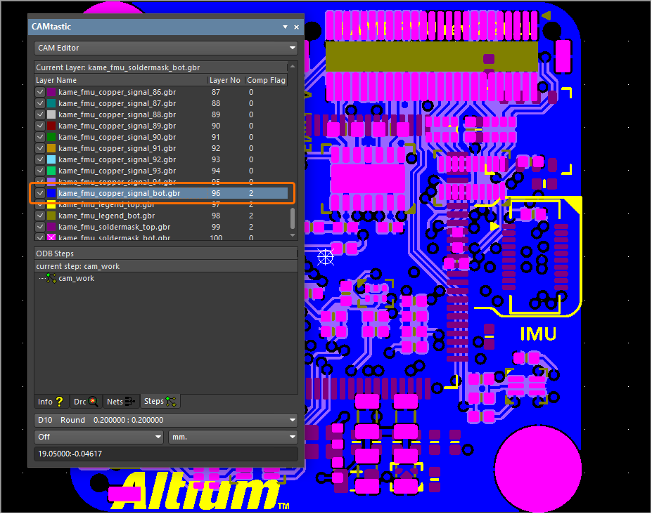
Автоматическое назначение цветов для импортируемых файлов Gerber и ODB++
Цвета слоев теперь назначаются в соответствии с типом слоя (например, красный для signal-top, синий для signal-bottom и т. д.) при импорте файлов Gerber и ODB++ в редактор CAM, если в импортируемых файлах отсутствует информация о цвете слоев. Новая функция цветов по умолчанию реализована для исключения ситуаций, когда слоям могли быть назначены неправильные цвета.
Для получения дополнительной информации см. страницу Preparing Fabrication Data.
Улучшение проектирования жгутов
Возможность «разделения» таблицы соединений
Таблица соединений расширенного проекта жгута может содержать большое количество записей, которые бывает трудно разместить в чертежном документе в виде одной таблицы. Вместо масштабирования шрифта и таблицы, создания нескольких пользовательских записей таблицы или использования внешнего документа теперь можно «разделить» таблицу соединений в документе Harness Draftsman (*.HarDwf), чтобы она отображалась на нескольких «страницах». На панели Properties для размещенной таблицы соединений включите параметр Limit Page Height в области Pages , чтобы использовать новую функцию. Это ограничит высоту таблицы соединений указанным значением высоты (Max Page Height) и, следовательно, количеством строк, отображаемых в таблице.
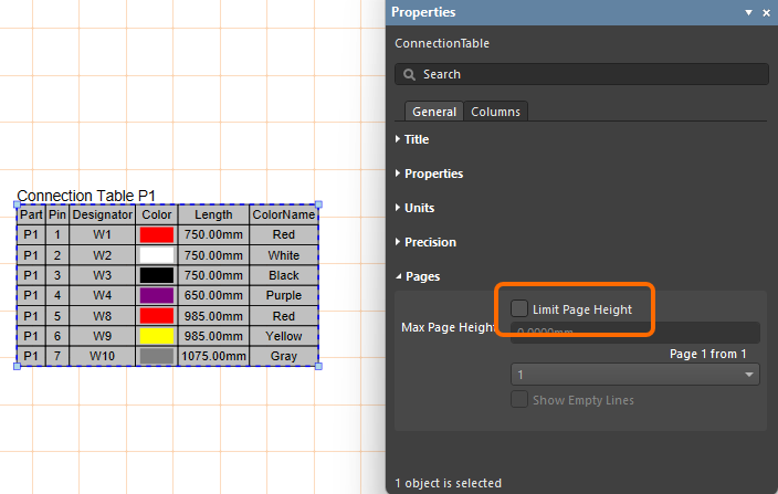
Редактор определяет, что отображается не вся таблица соединений, о чем свидетельствует запись Page на панели (например, 1 from 2), а соответствующее раскрывающееся меню позволяет указать, какая страница отображается. Чтобы добавить дополнительные страницы таблицы соединений, разместите еще одну таблицу соединений (Place » Connection Table) и задайте следующую Page в области Pages панели Properties .

Для получения дополнительной информации см. страницу Creating a Manufacturing Drawing for a Harness Design.
Улучшения управления данными
Добавлена поддержка типа данных «Temperature Coefficient»
При определении пользовательского параметра как части шаблона компонента в подключенном Workspace на платформе Altium теперь поддерживается дополнительный тип данных с учетом единиц измерения – Temperature coefficient (ppm/°C).

Параметры, использующие этот новый тип единиц, поддерживаются в различных областях программы, включая панель Components panel, редактор компонентов (как в режиме single, так и в режиме batch), а также функциями Library Importer и Components Synchronization (в разделе Parameter Mapping панели Properties).
Для получения дополнительной информации о типах данных параметров компонентов с учетом единиц измерения см. страницу Component Templates.
Возможность изменить примененную конфигурацию среды
При подключении к Workspace платформы Altium, в котором определены Environment Configurations, и если пользователь назначен нескольким группам (то есть может применяться несколько конфигураций среды), теперь можно изменить применяемую конфигурацию после первоначального выбора и включения параметра Remember my choice в диалоговом окне Select a Configuration. Для этого предусмотрено новое диалоговое окно Connection Properties, доступное из меню Properties для Workspace на странице Data Management - Servers page окна Preferences, которое позволяет быстро изменить используемую конфигурацию из числа доступных вам.

Для получения дополнительной информации о применении конфигураций среды см. страницу Accessing Your Workspace.
Улучшение импорта/экспорта
Расширенный мастер импорта Allegro (открытая бета-версия)
В этом выпуске представлен улучшенный мастер импорта Allegro, который поддерживает импорт масок припоя и пасты на уровне padstack для контактных площадок (обычных и пользовательской формы, включая tented pads) и переходных отверстий (с расчетом расширений и учетом tented-сторон).
Кроме того, при импорте проекта Allegro с перечисленными ниже определенными подклассами на слоях Top или Bottom в создаваемом PCB-документе теперь формируется пара слоев компонентов для размещения значений с этих слоев Top и Bottom; при этом по умолчанию эти слои скрыты с точки зрения видимости.
Подкласс проекта Allegro |
Пара слоев компонентов Altium |
|---|---|
Layers - Components - Comp value |
COMPONENT_VALUE_TOP и COMPONENT_VALUE_BOTTOM |
Layers - Components - Dev type |
DEVICE_TYPE_TOP и DEVICE_TYPE_BOTTOM |
Layers - Components - Tolerance |
TOLERANCE_TOP и TOLERANCE_BOTTOM |
Layers - Components - User part |
PART_NUMBER_TOP и PART_NUMBER_BOTTOM |
Для получения дополнительной информации см. страницу Importing a Design from Allegro.
Функция стала полностью общедоступной в Altium Designer 26.6
Следующая функция с этим выпуском официально стала общедоступной:
Версия 26.5
Altium Designer Develop – Released: 6 May 2026, Version 26.5.1 (build 12) – Additional Update
Altium Designer Agile – Released: 6 May 2026, Version 26.5.1 (build 30) – Additional Update
Altium Designer – Released: 6 May 2026, Version 26.5.1 (build 12) – Additional Update
Altium Designer Develop – Released: 8 April 2026 – Version 26.5.0 (build 11)
Altium Designer Agile – Released: 8 April 2026 – Version 26.5.0 (build 17)
Altium Designer – Released: 8 April 2026 – Version 26.5.0 (build 11)
Примечания к выпуску Altium Designer
Key Highlights
Улучшение редактора схем
Добавлена возможность задавать вертикальный отступ вывода
Теперь можно задавать пользовательский вертикальный отступ для обозначения и имени вывода. Это дает полный контроль над горизонтальными (X) и вертикальными (Y) отступами. Отступы можно задать глобально на странице Schematic - General диалогового окна Preferences в области Pin Settings в полях Designator и Margin (X/Y). Чтобы задать отступы локально, используйте поля Margin (X/Y) на панели Properties .
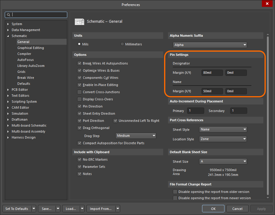
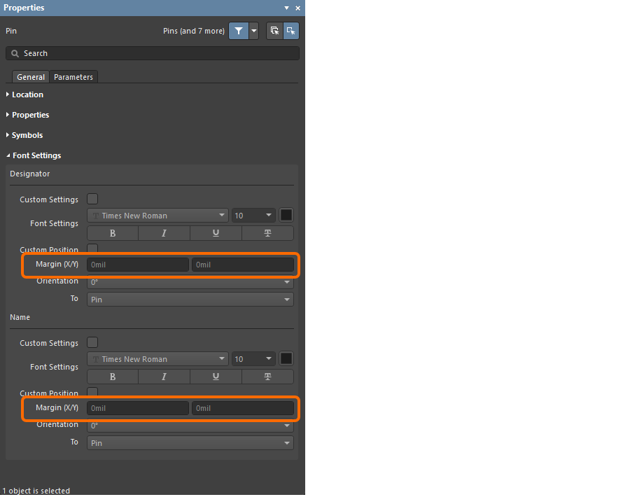
Вертикальный отступ вывода задается с помощью новых полей Pin Designator Vertical Margin и Pin Name Vertical Margin на панелях List и в диалоговом окне Find Similar Objects. Кроме того, в категории SCH Functions\Fields доступны два новых ключевых слова запросов — PinDesignator_CustomPosition_VerticalMargin и PinName_CustomPosition_VerticalMargin — для адресации вертикального отступа этих двух свойств при создании логических выражений запросов.
Для получения дополнительной информации см. страницу Creating a Schematic Symbol.
Улучшение проектирования PCB
Защита интеллектуальной собственности ODB++ (открытая бета-версия)
В этом выпуске появилась возможность настраивать параметры ODB++ для защиты вашей ценной интеллектуальной собственности (IP) путем ограничения того, что будет генерироваться.
В диалоговом окне ODB++ Setup можно выбрать, какие сигнальные слои экспортировать в составе создаваемых данных. Кроме того, можно управлять включением списка соединений и, если он включен, выполнять его нейтрализацию (заменяя имена цепей на Net_[1-…]). Также можно управлять включением компонентов, с возможностью удаления свойств компонентов (параметров).

Информация о пути к папке также будет удаляться из создаваемых файлов отчета ([Design name].REP) и правил (odb\user\[Design name].RUL).
Для получения дополнительной информации о подготовке производственных данных ODB++ см. страницу Preparing Fabrication Data.
Улучшение Wire Bonding
Улучшения 3D для Wire Bonding (открытая бета-версия)
В этом выпуске добавлена расширенная поддержка bond wire в 3D-виде платы. В частности:
-
Дополнительные элементы редактирования для определения формы/профиля bond wire. Теперь можно указать начальный Angle (α) и конечный Angle (β).
Параметр Die Bond Type был переименован в Type, с более интуитивно понятным выбором, отражающим начало и конец bond wire (либо Ball - Wedge или Wedge - Wedge). Также появилась возможность включить и указать Override Color для bond wire. Это позволяет различать разные «уровни» bond wire, связанные с различными циклами работы машины wire bonding, при создании схемы сборки wire bonding.

-
Возможность размещать контактные площадки кристалла и проволочные выводы на универсальных 3D-телах (форматы моделей STEP, SOLIDWORKS Part и Parasolid, а также выдавленные 3D-тела). При размещении на универсальном 3D-теле контактные площадки кристалла будут автоматически размещаться на высоте тела под центром площадки.

В этом примере в качестве кристалла используется модель в формате Parasolid. -
Включение объектов проволочных выводов в проверку Component Clearance для обнаружения нарушений зазоров между проволочными выводами и другими (не являющимися проволочными выводами) объектами в 3D-пространстве.

Пример обнаруженного столкновения между проволочным выводом и 3D-телом. -
Объекты проволочных выводов теперь также включаются при экспорте PCB в форматы STEP и Parasolid.
Кроме того, цвета, используемые для проволочных выводов в проекте PCB, теперь учитываются при размещении вида изготовления платы, сборочного вида платы и вида компонента в производственном чертеже PCB (*.PCBDwf). Можно выбрать использование цвета слоя или переопределенного цвета (если он задан для проволочных выводов на стороне PCB).


Кроме того, при использовании расширенной поддержки проволочных выводов доступны следующие возможности:
-
Bond Wires доступен как объект в Selection Filter, вызываемом из Active Bar и панели Properties (фильтрация до и после выбора) –
 .
.
-
Bond Wire добавлен как отдельный тип объекта (при фильтрации отображения объектов) как в панели PCB List, так и в панели PCBLIB List –
 .
.
-
При использовании Layer Sets слои Die и Wire Bonding теперь входят в набор слоев Signal Layers –
 .
.
Дополнительную информацию о Wire Bonding см. на странице Wire Bonding.
Улучшения управления данными
Улучшенная панель Design Reuse (Open Beta)
Эта функция предоставляет вам новую улучшенную панель Design Reuse при работе с блоками повторного использования и сниппетами.

Дополнительную информацию см. на странице Working with Reuse Blocks.
Улучшенное управление моделями посадочных мест в Item Manager
Модуль Item Manager был улучшен для обработки случая, когда компонент Workspace имеет несколько определенных моделей посадочных мест, а имя текущей назначенной модели впоследствии изменяется.
Компонент Workspace может иметь несколько назначенных моделей посадочных мест. Если имя текущей назначенной модели посадочного места впоследствии изменено и сохранено обратно в Workspace (что создает новую ревизию модели посадочного места), а затем сам компонент Workspace сохранен обратно в Workspace (создавая новую ревизию компонента, использующую новую ревизию модели посадочного места), экземпляры этого компонента, уже размещенные в проекте, требуют обновления до последней ревизии. В этом случае можно использовать команды Automatch и Update to latest revision модуля Item Manager. Теперь эти функции корректно назначают последнюю ревизию модели посадочного места, имя которой было изменено.


Дополнительную информацию о Item Manager см. на странице Managing Content with the Item Manager.
Проверка последней ревизии при пакетном редактировании компонентов
Проверка правила компонента Revision that is being edited is not latest теперь корректно выполняется при редактировании одного или нескольких компонентов Workspace с помощью редактора компонентов в режиме Batch Component Editing mode. Это гарантирует, что нарушения будут отмечены при редактировании компонента, который не является последней доступной ревизией в Workspace.
В показанном ниже примере в редакторе компонентов в режиме Batch Component Editing редактируются четыре ревизии компонентов. Ни одна из этих ревизий не является последней (то есть в Workspace доступны более поздние ревизии этих компонентов), и для каждой ревизии отмечается нарушение.

Дополнительную информацию о проверке компонента перед сохранением в Workspace см. на странице Validating a Component.
Функция, полностью переведенная в статус Public в Altium Designer 26.5
Следующая функция с этим выпуском официально получила статус Public:
Дополнительная функция в Altium Designer 26.5
-
Частичная поддержка LFS-репозиториев: В этом выпуске в диалоге
VCS.AllowLFSReposдоступен новый параметр расширенных настроек Advanced Settings dialog, который при включении восстанавливает прежнюю частичную возможность использования LFS-репозиториев при работе с системой контроля версий Git. ВНИМАНИЕ: Altium Designer не полностью поддерживает работу с LFS-репозиториями, и в некоторых случаях это может привести к потере пользовательских данных.
Версия 26.4
Altium Designer Develop – Released: 19 March 2026 – Version 26.4.1 (build 13)
Altium Designer Agile – Released: 19 March 2026 – Version 26.4.1 (build 25)
Altium Designer – Released: 19 March 2026 – Version 26.4.1 (build 12)
Примечания к выпуску Altium Designer
Key Highlights
Улучшение проектирования PCB
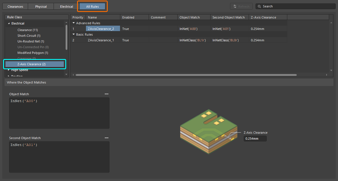
Z-Axis Clearance (Open Beta)
В этом выпуске добавлено новое правило проектирования Z-Axis Clearance как в Constraint Manager, так и в старый диалог PCB Rules and Constraints Editor (недоступный в Document View). Это правило, входящее в категорию Electrical, может использоваться для проверки минимальных зазоров между различными примитивами на разных медных слоях.

В Constraint Manager ограничение Z-Axis Clearance можно задать при определении электрических зазоров между классами цепей и/или дифференциальных пар (из представления Clearances), а также путем добавления нового расширенного правила этого типа (из представления All Rules, когда доступ к Constraint Manager осуществляется из PCB).
![]()
Также можно добавить правило этого типа в директиву набора параметров при ее размещении на схеме.

Новое правило поддерживается как Online, так и Batch DRC (для Batch DRC включено по умолчанию), а также связанными механизмами отображения нарушений (details/overlay — оба также отключены по умолчанию). Если для правила включено отображение Violation Details (на странице PCB Editor – DRC Violations Display диалога Preferences), текст в рабочем пространстве PCB отображается в формате:
< [RuleValue] ([Actual Z-Axis Clearance Value]; XY: [Z-Axis Clearance Projected on XY])
Где [RuleValue] — это ограничение, заданное в правиле, а [Actual Z-Axis Clearance Value] — кратчайшее диагональное расстояние между краями примитивов на разных слоях.
В других местах программы используется следующий формат:
Z-Axis Clearance: ([Actual Z-Axis Clearance Value] < [RuleValue]) Between [Object1Description] And [Object2Description]

Новое правило также поддерживается для:
-
Полигональных заливок (сплошных и штриховых) и внутренних плоскостей
-
Функции PCB CoDesign
Дополнительную информацию см. на странице Electrical Rule Types.
Улучшение Constraint Manager
Добавлены минимальные, максимальные и предпочтительные значения для диаметра и размера отверстия
Теперь при определении правила Routing Via Style в представлении Physical можно задавать отдельные минимальные (Min), максимальные (Max) и предпочтительные (Preferred) значения для Diameter и Hole Size в дополнение к определению по предпочтительному шаблону. Это позволяет задавать более точные ограничения.
Кроме того, при доступе к Constraint Manager из PCB или при настройке ограничений для конкретного стека слоев теперь можно переключаться между развернутым представлением Min/Max Preferred и представлением Templates , выбирая нужную вкладку.
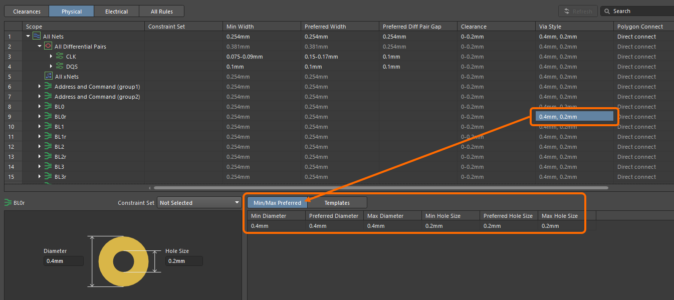
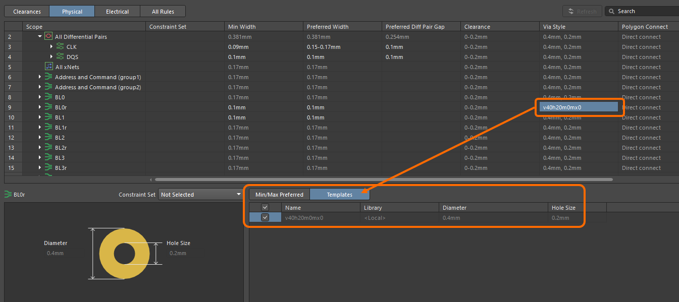
Для получения дополнительной информации см. страницу Defining Design Requirements Using the Constraint Manager.
Улучшения в управлении данными
Объединение данных поставщиков (Open Beta)
В этом выпуске представлено важное улучшение при использовании функции синхронизации Custom Parts Provider в Altium Designer (подробнее) для сопоставления данных поставщиков из указанного источника базы данных с данными цепочки поставок Workspace.
Данные поставщиков из настроенного Custom Parts Provider теперь объединяются с Altium Parts Provider, чтобы везде, где в интерфейсе программы отображаются данные поставщиков (SPN), показывалась совокупная информация обо всех поставщиках, включая панель Manufacturer Part Search, ActiveBOM и добавление вариантов компонентов.


Для получения дополнительной информации о синхронизации базы данных цепочки поставок с данными Workspace см. страницу Supply Chain Database to Workspace Data Synchronization.
Возможность изменять состояние жизненного цикла из ActiveBOM
Теперь вы можете изменять состояние жизненного цикла выбранных компонентов непосредственно в документе ActiveBOM (*.BomDoc). Новая команда Change State доступна в подменю Operations, открываемом правой кнопкой мыши в ActiveBOM.
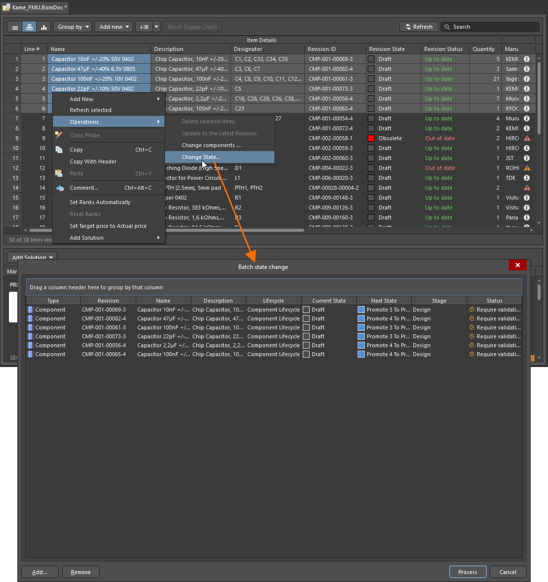
Для получения дополнительной информации см. страницу Managing Item Revision Lifecycle.
Изменения интерфейса расширенных настроек общего доступа
При предоставлении общего доступа к live design или снимку проекта через диалоговое окно Share прежнее окно, открывавшееся с помощью элемента управления Advanced Settings, было переработано в виде всплывающего окна.
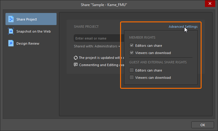
При предоставлении общего доступа к live design параметры совместного использования и скачивания теперь сгруппированы по Member Rights (для участников Workspace) и Guest and External Share Rights (для внешних гостевых пользователей, с которыми проекты были общими). Подтверждение изменений выполняется нажатием специальной кнопки ![]() в основном диалоговом окне Share.
в основном диалоговом окне Share.
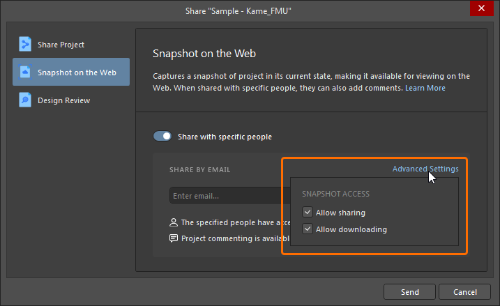
Для получения дополнительной информации о совместном использовании проектов см. страницу Sharing a Design.
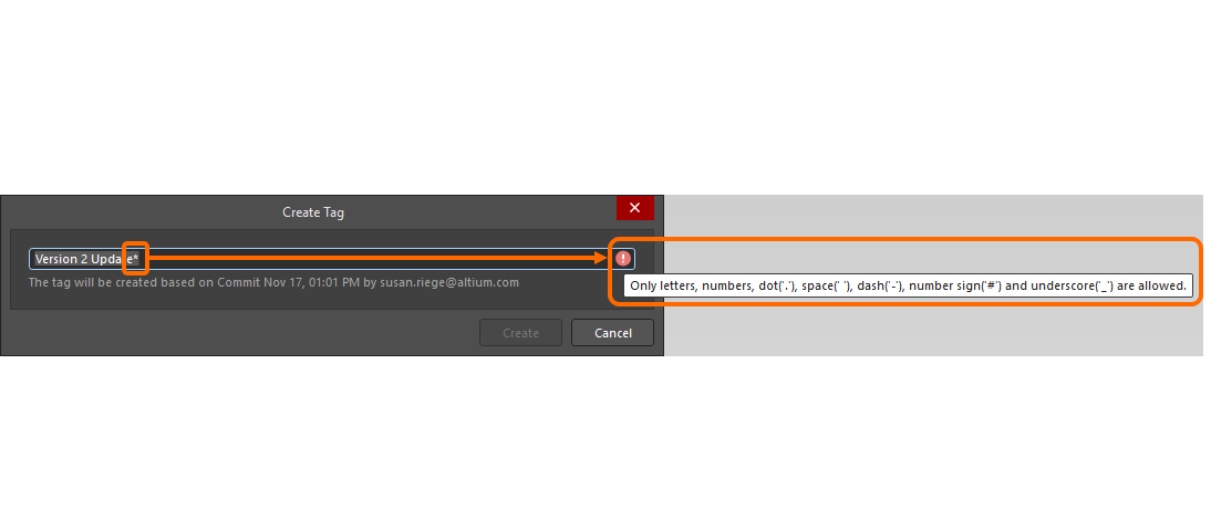
Улучшенная команда 'Create Tag'
Команда Create Tag была восстановлена в подменю History & Version Control. Команда также была улучшена при вводе значения для тега. Если используется недопустимый символ, в диалоговом окне Create Tag появляется значок ![]() . Наведите курсор на значок, чтобы увидеть подсказку о том, какие символы разрешены, а именно: буквы, цифры, точка ('.'), дефис ('-'), знак номера ('#') и подчеркивание ('_'); при необходимости обновите тег.
. Наведите курсор на значок, чтобы увидеть подсказку о том, какие символы разрешены, а именно: буквы, цифры, точка ('.'), дефис ('-'), знак номера ('#') и подчеркивание ('_'); при необходимости обновите тег.
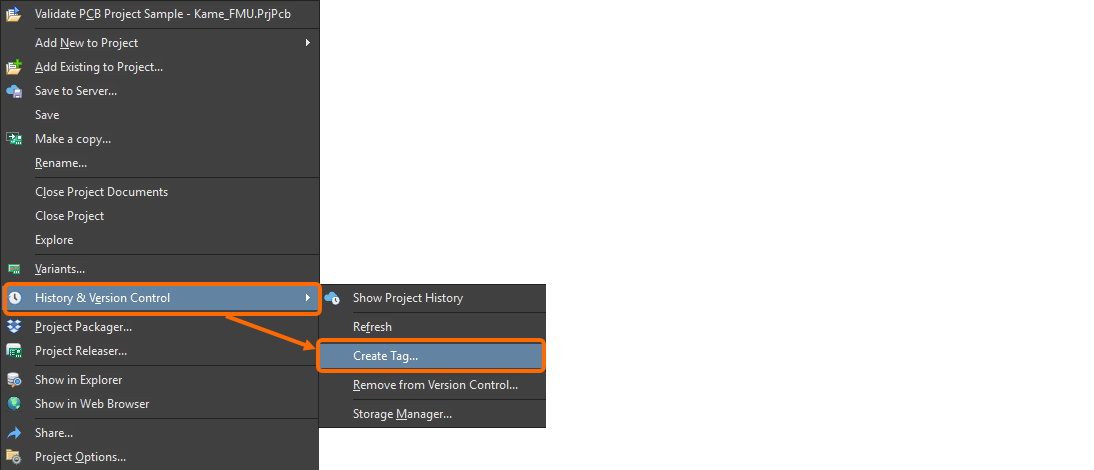
Для получения дополнительной информации см. страницу Browsing the History of a Project.
Поддержка баз данных PostgreSQL в функциях синхронизации
Функции синхронизации Custom Parts Provider и Components Synchronization в Altium Designer были улучшены и теперь поддерживают базы данных PostgreSQL.
Для получения дополнительной информации о функциях синхронизации см. страницы Component Database to Workspace Data Synchronization и Supply Chain Database to Workspace Data Synchronization.
Улучшение BOM CoDesign
Улучшенная команда 'Explore Suggested Component'
При использовании функции BOM CoDesign, и в частности команды Explore Suggested Component (из раздела Differences панели Properties), если предложенный компонент не является последней ревизией, теперь в панели Components будет открываться именно эта ревизия.
, команда Explore Suggested Component теперь открывает предложенную ревизию в панели Components.")
Хотя предложенная ревизия компонента CMP-009-00009-5 не является последней (в библиотеке существует ревизия CMP-009-00009-6 того же компонента), команда Explore Suggested Component теперь открывает предложенную ревизию в панели Components.
Для получения дополнительной информации о функции BOM CoDesign см. страницу BOM CoDesign.
Функция стала полностью публичной в Altium Designer 26.4
Следующая функция теперь официально имеет статус Public в этом выпуске:
Дополнительные функции в Altium Designer 26.4
-
Библиотека Open CASCADE для документов Multi-board Assembly (Open Beta): В этом выпуске в диалоговом окне Advanced Settings dialog доступен новый параметр расширенных настроек –
System.MBAEngine.UseOpenCascade– который при включении переключает геометрическое моделирование документа multi-board assembly (*.MbaDoc) с библиотеки C3D на библиотеку Open CASCADE. Обратите внимание, что при открытии в этом выпуске более старого документа multi-board assembly (из предыдущей версии ПО) с включенной опцией созданные сопряжения будут удалены. Вы можете выбрать сохранение относительных положений частей сборки или размещение их в линию. Во время открытия у вас будет возможность создать резервную копию старой версии. -
JSON Web Token (Open Beta): В этом выпуске в диалоговом окне Advanced Settings dialog доступен новый параметр расширенных настроек –
EDMS.CloudLoginByJWT– который при включении использует JWT (JSON Web Token) для идентификации и аутентификации пользователя при подключении из Altium Designer к Workspace на Altium Platform.
Версия 26.3
Altium Designer Develop – Released: 5 February 2026 – Version 26.3.0 (build 5)
Altium Designer Agile – Released: 5 February 2026 – Version 26.3.0 (build 18)
Altium Designer – Released: 5 February 2026 – Version 26.3.0 (build 6)
Примечания к выпуску Altium Designer
Key Highlights
Улучшение проектирования печатных плат
Расширенная поддержка форматов SOLIDWORKS и Parasolid
-
Добавлена поддержка моделей SOLIDWORKS 2024 и 2025 (
*.SldPrt) при работе с 3D bodies. -
Экспорт печатной платы в формат файла Parasolid (
*.x_t) теперь использует версию Parasolid 35.1. Это позволяет более поздним версиям SOLIDWORKS (2024 и 2025) корректно открывать/импортировать файл.
Для получения дополнительной информации см. страницу Mechanical Data Import-Export Support.
Улучшения проектирования жгутов
Отображение перемычек
Перемычки, заданные в монтажной схеме, теперь корректно учитываются в связанном чертеже компоновки. Перемычка соединяет две полости одного и того же разъема. Если на чертеже компоновки выбран жгут, область Bundle Objects панели Properties теперь включает такие перемычки, которые начинаются и заканчиваются в одной и той же точке подключения как часть этого жгута.
Для таких проводов будет доступна только возможность вручную задать их длину. Введенное значение затем будет включено в документ ActiveBOM проекта жгута и производственный чертеж (таблицу BOM и список проводов).


Для получения дополнительной информации см. страницу Creating the Layout Drawing.
Улучшенная функция 'Update From Libraries'
Обновление из библиотек (Tools » Update From Libraries) было улучшено для монтажных схем (*.WirDoc) и чертежей компоновки (*.LdrDoc) проектов жгутов.
-
Когда эта функция вызывается из монтажной схемы, теперь также включаются провода, компоненты полостей и связанные детали.

-
Когда эта функция вызывается из чертежа компоновки, теперь также включаются покрытия жгутов, метки компоновки и связанные детали.

Для получения дополнительной информации см. страницы Defining the Wiring Diagram и Creating the Layout Drawing.
Улучшение платформы
Master Services Agreement заменяет EULA
Лицензионное соглашение с конечным пользователем (EULA) было заменено на Основное соглашение об оказании услуг (MSA) при установке Altium Designer Develop или Altium Designer Agile.


Для получения дополнительной информации см. страницы Установка и управление Altium Designer Develop и Установка и управление Altium Designer Agile.
Версия 26.2
Altium Designer Develop – Released: 8 January 2026 – Version 26.2.0 (build 10)
Altium Designer Agile – Released: 8 January 2026 – Version 26.2.0 (build 28)
Altium Designer – Released: 8 January 2026 – Version 26.2.0 (build 7)
Примечания к выпуску Altium Designer
Key Highlights
Улучшения Wire Bonding
Поддержка панелизированных PCB
Проволочные соединения и контактные площадки кристалла теперь отображаются при просмотре документа панелизированной PCB в 3D.

Кроме того, теперь поддерживается создание отчета Wire Bonding Table Report из документа панелизированной PCB.
Для получения дополнительной информации о панелизированных PCB см. страницу Board Panelization.
Новое ключевое слово запроса для обнаружения проволочных соединений
При построении логических выражений запросов для использования при фильтрации объектов в PCB/PcbLib или при задании области действия правила проектирования теперь доступно новое IsBondwire ключевое слово запроса (проверка типа объекта PCB).

Для получения дополнительной информации см. страницу Object Type Checks.
Улучшение проектирования жгутов
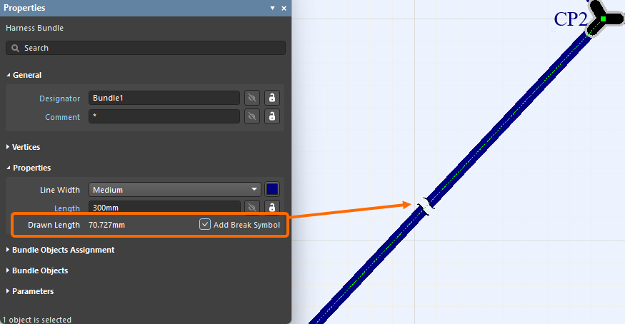
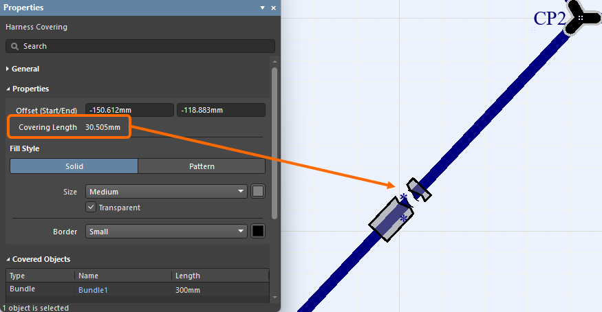
Возможность размещения точки разрыва пучка жгута
Точку разрыва, которая используется как указание того, что пучок не в масштабе (NTS), теперь можно разместить на пучке жгута на чертеже компоновки жгута (*.LdrDoc). Пучок будет отображать символ разрыва посередине своего самого длинного сегмента, как показано на первом изображении ниже, а в свойствах будет отображаться Drawn Length, , что отражает длину пучка, как она нарисована в рабочем пространстве проекта. Обычно физическая длина пучка будет значительно больше. Когда задано поле Length (фактическая физическая длина) и оно отличается от нарисованной длины, пучок будет отображать символ разрыва в центре своего самого длинного сегмента, указывая, что пучок не в масштабе (NTS). Чтобы разместить разрыв, включите параметр Add Break Symbol в области Properties свойств пучка. Покрытия жгута, которые покрывают пучок жгута с точкой разрыва, также будут отображать разрыв в том же месте. Если покрытие жгута заканчивается в точке разрыва пучка жгута, покрытие будет нарисовано немного длиннее, как показано на втором изображении.
Для получения дополнительной информации см. страницу Creating the Harness Layout Drawing.
Улучшение управления данными
Возможность сохранять состояние жизненного цикла при синхронизации компонентов
В этом выпуске у вас появилась возможность сохранять состояние жизненного цикла при выполнении синхронизации компонентов между вашим Workspace и вашей базой данных компонентов с использованием функции синхронизации компонентов Altium Designer.
Эта возможность обеспечивается новым параметром Preserve lifecycle state. Когда источник данных (таблица) выбран в документе Components Synchronization Configuration (*.CmpSync), этот параметр можно найти в разделе Advanced панели Properties.

Обратите внимание, что эта возможность доступна для тех, кому назначено операционное разрешение Allow to skip lifecycle state change for new revisions (подробнее см. в разделе Setting Global Operation Permissions for a Workspace).
Для получения дополнительной информации о функции синхронизации компонентов см. страницу Component Database to Workspace Data Synchronization.
Функции, ставшие полностью общедоступными в Altium Designer 26.2
Следующие функции в этом выпуске теперь официально имеют статус Public:
-
BOM CoDesign — доступно с версии 25.1
-
Исключение полей, связанных с поставщиками, из результата сравнения BOM — доступно с версии 26.1
Версия 26.1
Altium Designer Develop – Released: 3 December 2025 – Version 26.1.0 (build 6)
Altium Designer Agile – Released: 3 December 2025 – Version 26.1.0 (build 13)
Altium Designer – Released: 3 December 2025 – Version 26.1.0 (build 7)
Примечания к выпуску Altium Designer
Key Highlights
Улучшение проектирования PCB
Значение по умолчанию для правила расширения паяльной маски теперь 0 mils (Open Beta)
В соответствии со стандартом IPC-7351B относительно значений padstack по умолчанию, где окна паяльной маски обычно имеют соотношение 1:1 к размеру контактной площадки, значения для правила Solder Mask Expansion (в документах PCB) и управляемого правилом расширения паяльной маски (в документах библиотек PCB) теперь по умолчанию установлены в 0 mil вместо прежних 4 mil.
Для библиотеки PCB (*.PcbLib) поддержка этих новых значений по умолчанию реализована на уровне библиотеки и наследуется всеми посадочными местами компонентов, созданными в ней. Одна и та же PCBlib будет показывать расширение 4 mil для всех объектов с управляемым правилами расширением паяльной маски при открытии в предыдущей версии Altium Designer и расширение 0 mil при открытии в этом и более поздних выпусках, как показано ниже для объекта pad.

Для документа PCB (*.PcbDoc) все существующие правила Solder Mask Expansion сохраняют свои исходные значения. Значения по умолчанию, используемые для любого вновь создаваемого правила, определяются версией Altium Designer, в которой это правило было создано, и не будут изменяться при открытии в другой версии Altium Designer. Таким образом, по умолчанию будет расширение 4 mil для правил, созданных в предыдущей версии Altium Designer и открытых в любой другой версии, и расширение 0 mil для правил, созданных в этом выпуске (или позже) и открытых в любой другой версии, как показано ниже.

Новое правило проектирования Solder Mask Expansion, созданное в Constraint Manager.

Новое правило проектирования Solder Mask Expansion, созданное в диалоговом окне PCB Rules and Constraints Editor.
Для получения дополнительной информации о правиле проектирования Solder Mask Expansion см. страницу Mask Rule Types.
Улучшение Constraint Manager
Добавлена возможность фильтрации классов
В представлении Clearances Constraint Manager реализована возможность фильтрации классов, чтобы упростить работу с большим количеством классов. Это позволяет создавать фильтры (или группировки) классов для переключения между сфокусированными подмножествами матрицы зазоров и работы с ними.
Используйте кнопку ![]() в правом верхнем углу представления Clearances, чтобы открыть всплывающее окно, в котором можно создавать, редактировать, удалять, а также включать/отключать фильтры.
в правом верхнем углу представления Clearances, чтобы открыть всплывающее окно, в котором можно создавать, редактировать, удалять, а также включать/отключать фильтры.
![]()
Чтобы создать новый фильтр, нажмите кнопку ![]() , а затем нажмите кнопку
, а затем нажмите кнопку ![]() во всплывающем окне.
во всплывающем окне.
![]()
Задайте уникальное имя для нового фильтра, включите требуемую группу классов и нажмите ![]() .
.
![]()
После создания фильтра используйте доступные элементы управления во всплывающем окне, чтобы при необходимости включать, отключать, редактировать или удалять его. Обратите внимание, что когда фильтр включен, кнопка в правом верхнем углу отображается как ![]() .
.
Для получения дополнительной информации о работе с матрицей зазоров см. страницу Defining Design Requirements Using the Constraint Manager.
Улучшение Draftsman
Расширенный импорт DXF в документы Draftsman (Open Beta)
Эта функция добавляет поддержку импорта файлов DXF версии R12 и более поздних в документы производственных чертежей (*.PCBDwf, *.HarDwf, *.MbDwf). Теперь также поддерживается импорт файлов DXF, содержащих сплайны.
Для получения дополнительной информации об импорте файлов DXF см. страницу Draftsman Placement & Editing Techniques.
Улучшение Wire Bonding
Примитивы bond wire в панелях
Проволочные соединения теперь представлены с корректным типом (Bond Wire) в следующих местах:
-
Область Primitives панели PCB, когда выбран компонент в режиме Nets mode
-
Область Component Primitives панели PCB, когда выбрана цепь в режиме Components mode
-
Панель PCB Library panel, когда выбрано посадочное место.
Выбор примитива проволочного соединения приведет к выбору/подсветке этого проволочного соединения в рабочем пространстве проекта.


Кроме того, в контекстном меню области, вызываемом правой кнопкой мыши, теперь доступен соответствующий параметр Show Bond Wires для переключения видимости проволочных соединений.
Для получения дополнительной информации о wire bonding см. страницу Wire Bonding.
Улучшение проектирования 3D-MID
Проверка правил проектирования 3D-MID (Open Beta)
В этом выпуске реализована пакетная проверка правил проектирования (DRC) для нарушений правил ширины, зазора, длины и согласованных длин применительно к трассам, проложенным на вашей 3D-подложке. Обратите внимание, что хотя сгенерированный отчет DRC будет содержать информацию по всем этим проверкам, в рабочем пространстве проекта будут подсвечиваться только нарушения зазоров.


Для получения дополнительной информации см. страницу 3D-MID Design.
Улучшение multi-board проектирования
Возможность задавать «Termination Type» для элементов жгута
Параметр Termination Type для элемента жгута теперь можно задавать в multi-board схеме. Доступны следующие типы оконцовки:
-
Connector – стандартный вариант, используемый при подключении к ответному разъему на PCB. Обычно предполагает применение стандартных разъемов, устанавливаемых на плату.
-
Crimps/Ferrules – отдельные провода оканчиваются обжимами или втулочными наконечниками перед установкой в разъем со стороны PCB.
-
Wire termination – провода обрезаются вровень на конце жгута и затем либо закрепляются винтом, либо припаиваются непосредственно к PCB. Это типично для прямых соединений провод-плата, например с некоторыми разъемами JST.
Эта информация отображается в свойствах выбранного элемента жгута и соответствующего элемента модуля.


Подробнее о работе с соединениями в multi-board схеме см. на странице Working with Connections.
Улучшения проектирования жгутов
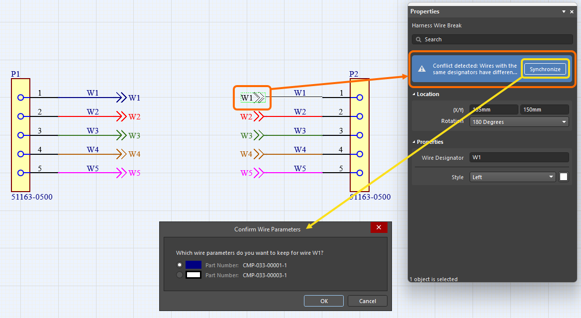
Улучшенная синхронизация проводов
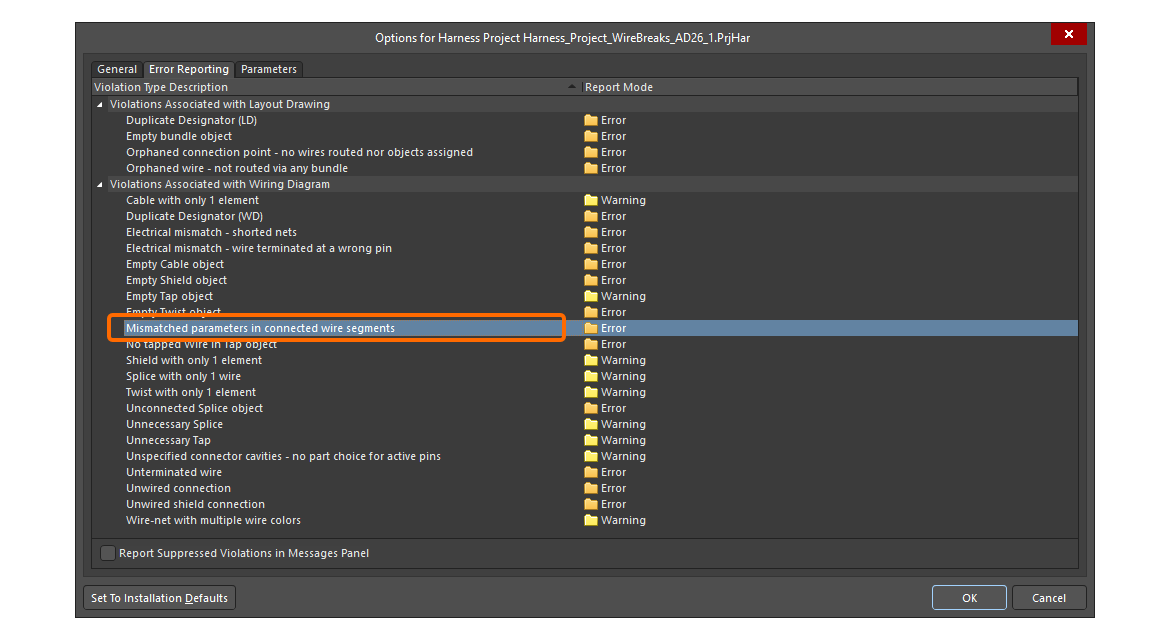
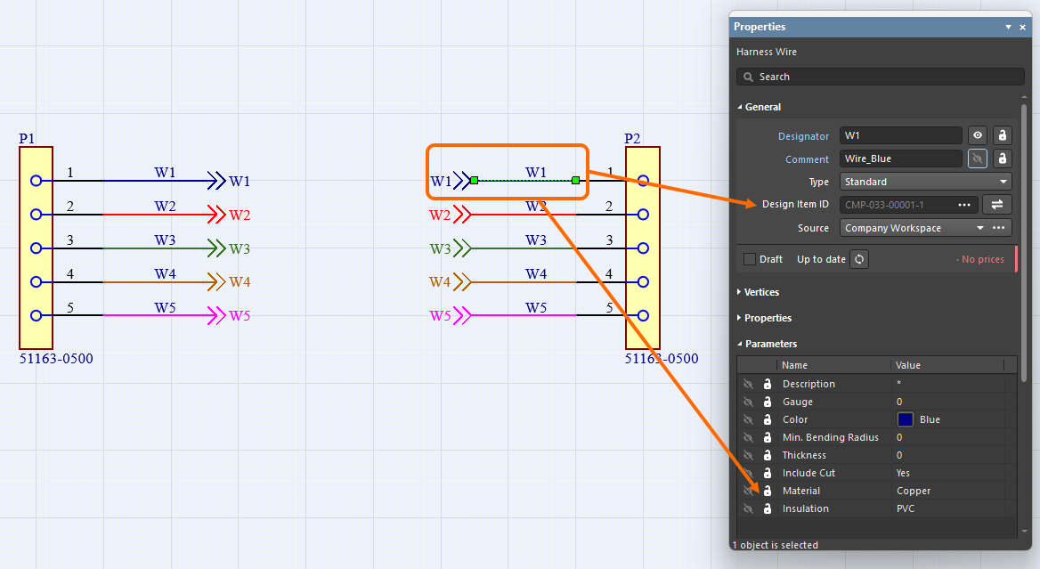
Провода жгута, соединенные через разрыв провода, теперь распознаются даже в том случае, если у них разные Design Item ID. Кроме того, теперь сравниваются все сегменты провода с одинаковым обозначением, соединенные одним и тем же разрывом провода (по номеру детали, комментарию, цвету и всем параметрам). При обнаружении любых различий выдается нарушение Mismatched parameters in connected wire segments. Также в панели Properties для провода и разрыва провода появляется предупреждение о том, что обнаружен конфликт параметров. Нажмите Synchronize в предупреждении, чтобы открыть диалоговое окно Conflict Wire Parameters, где можно выбрать, какие параметры использовать для сегмента провода.
Возможность размещать покрытие поверх точки соединения
Теперь на чертеже компоновки жгута (*.LdrDoc) можно применять/продлевать покрытие жгута over точки соединения (точки соединения на чертеже компоновки, где сходятся два или более пучка). Это устраняет необходимость использовать отдельные покрытия жгута между точками соединения в секции, содержащей несколько разъемов.

Кроме того, началом покрытия теперь считается самая левая и верхняя точка его пути, а сам путь теперь включает только те пучки, на которых лежит покрытие.
Подробнее см. на странице Creating the Layout Drawing.
Поле Quantity в BOM изменено на «As Required» для некоторых объектов
Провода, кабели и покрытия жгута являются объектами с длиной как основной характеристикой, и их значение отображается в поле Length . Чтобы избежать путаницы, поле Quantity для записей проводов, кабелей и покрытий жгута в таблице Bill Of Materials и в документе ActiveBOM в производственном чертеже (*.HarDwf) теперь имеет значение As Required.

Подробнее см. на странице Managing Your Bill of Materials (BOM) with ActiveBOM.
Улучшенная группировка контактов в Wiring List
Улучшена группировка контактов в wiring list, размещаемом в документе производства жгута (*.HarDwf). Начиная с этой версии, автоматическая группировка применяется к разъему с наибольшим количеством проводов, и все его гнезда корректно группируются в столбце From wiring list, как показано на изображении ниже.

Книга Excel для производителей жгутов
Добавлена возможность генерировать через Output Job одну книгу Excel, содержащую данные для использования производителями жгутов. Для этого в разделе Report Outputs стал доступен новый генератор вывода — Manufacturing Data.

Сформированная книга включает четыре отдельных листа:
-
Bill of Materials – полезен для быстрого формирования коммерческого предложения.
-
Wiring List – для использования с машинами обработки проводов.
-
Labels – сводка физических этикеток для печати на пучках жгута, для использования с принтерами Zebra и другими.
-
Coverings – сводка покрытий, которые нужно нанести на пучки жгута.


Подробнее см. на странице Preparing Reports.
Улучшение платформы
Переход на .NET 8
В этой версии Altium Designer переходит с .NET 6 на .NET 8. Он поставляется в составе Altium Designer и позволяет использовать новые возможности и улучшения .NET, включая общее повышение производительности.
Подробнее см. на странице System Requirements.
WebView2 (Open Beta)
Начиная с этой версии, WebView2 используется для элементов, связанных с браузером, внутри Altium Designer (например, для страницы Home). Это обеспечивает доступ к новейшему движку веб-браузера в Altium Designer — достаточно просто обновить Windows.
Улучшения управления данными
Возможность копировать проект Workspace с использованием process workflow
Добавлена поддержка создания копии проекта Workspace с использованием заданных (и включенных) process workflow. Когда проект Workspace открыт, щелкните правой кнопкой мыши запись проекта в панели Projects и выберите активированное определение процесса (входящее в тему Project Creations) в подменю Make a copy of the managed project, чтобы начать копирование проекта в соответствии с базовым workflow этого процесса.

Подробнее см. на странице Process-based Project Creation.
Добавлена возможность сохранять состояние жизненного цикла при выпуске моделей
При выпуске новой ревизии модели компонента (schematic symbol, PCB footprint, simulation model или harness wiring) в подключенное Workspace теперь можно сохранить текущее состояние жизненного цикла модели.

Обратите внимание, что эта возможность доступна пользователям с назначенным операционным разрешением Allow to skip lifecycle state change for new revisions (подробнее см. Setting Global Operation Permissions for a Workspace).
Подробнее о редактировании содержимого Workspace см. на странице Creating & Editing Content.
Ссылки на комментарии в обзоре проекта
Когда комментарий добавляется в рамках design review, ссылка на этот обзор (From <DesignReviewName>) теперь отображается в соответствующей записи панели Comments And Tasks и в контекстном окне комментариев для этого комментария (в рабочем пространстве проекта). Нажмите ссылку, чтобы открыть страницу обзора Overview в новой вкладке браузера по умолчанию.

Подробнее о комментировании документов см. на странице Document Commenting.
Поддержка дополнительных типов данных с учетом единиц измерения
При определении пользовательского параметра в составе шаблона компонента в подключенном Workspace на платформе Altium теперь поддерживаются следующие дополнительные типы данных с учетом единиц измерения:
-
Площадь (mm2)
-
Бар (bar)
-
Бит
-
Кандела (cd)
-
Десятичное число
-
Целое число
-
Джоуль (J)
-
Люмен (lm)
-
Миллиметр (mm)
-
Паскаль (Pa)
-
Фунт на квадратный дюйм (psi)
-
Обороты в минуту (rpm)
-
Сименс (S)
-
Тесла (T)

Параметры, использующие эти новые типы единиц, поддерживаются в различных областях программного обеспечения, включая панель Components panel, редактор компонентов (в режимах single и batch), а также функцию Library Importer и функцию Components Synchronization (в разделе Parameter Mapping панели Properties).
Подробнее о типах данных параметров компонентов с учетом единиц измерения см. на странице Component Templates.
Возможность синхронизировать Part Choices при использовании Components Synchronization
Возможность определять и синхронизировать информацию о выборе деталей с помощью функции синхронизации компонентов и связанного с ней документа конфигурации синхронизации компонентов (*.CmpSync) была добавлена. Управление синхронизируемыми параметрами доступно в области Part Choices Mapping панели Properties, когда в документе выбрана таблица. Используйте кнопки для добавления и удаления пар параметров выбора деталей (Manufacturer / Part Number) и параметры раскрывающегося меню для определения сопоставления. Когда сопоставления заданы, соответствующие параметры отображаются в области сетки документа под столбцами Part Choice n.

Дополнительные сведения о функции синхронизации компонентов см. на странице Синхронизация данных базы компонентов с данными Workspace.
Новое предупреждение о проблемах при подключении к Workspace
Если возникает проблема с подключением к Workspace и не удается обновить последние состояния VCS документов проекта, элемент управления Refresh VCS Statuses (со связанным предупреждением во всплывающей подсказке) теперь отображается рядом с записью проекта на панели Projects. После восстановления соединения щелкните эту запись, чтобы снова синхронизировать состояния VCS и увидеть последние изменения.

Дополнительные сведения об индикации состояния документа см. на странице Управление документами проекта.
Улучшение BOM CoDesign
Исключение полей, связанных с поставщиками, из результата сравнения BOM (Open Beta)
При сравнении ActiveBOM с выбранным Managed BOM с помощью функции BOM CoDesign, если расширенная настройка отключена, данные, связанные с поставщиками (параметры Supplier и Supplier Part Number), исключаются из Differences section на вкладке Related BOMs панели Properties , если доступ к ней был получен из документа ActiveBOM.


Дополнительные сведения об анализе результатов сравнения см. на странице BOM CoDesign.
Улучшения импорта/экспорта
Улучшенный импорт проектов Allegro
Все необходимые файлы конфигурации теперь включены в файл Allegro2Altium.bat — пакетный файл, входящий в установку Altium Designer и используемый для преобразования бинарного файла Allegro (*.brd или *.dra) в формат ASCII (если такой проект/библиотека находится не на том же ПК, что и Altium Designer). Поэтому для импорта требуется только bat-файл, без каких-либо дополнительных файлов.
Дополнительные сведения см. на странице Импорт проекта из Allegro.
Поддержка альтернативных представлений компонентов из проектов xDX Designer
Теперь при импорте проекта xDX Designer поддерживаются альтернативные режимы представления компонентов как в создаваемых документах схем, так и в документах библиотек схем.
Дополнительные сведения см. на странице Импорт проекта из xDX Designer или DxDesigner.
Функции, ставшие полностью общедоступными в Altium Designer 26.1
Следующие функции теперь официально являются общедоступными в этом выпуске:
-
Подробный стек площадок для импортов Allegro - доступно с версии 25.7
-
Оптимизация панели Properties для свойств объектов PCB - доступно с версии 25.7
Дополнительные возможности в Altium Designer 26.1
-
Скрытые ссылки на внешние репозитории VCS (Open Beta): в этом выпуске в диалоговом окне Advanced Settings dialog доступен новый параметр расширенных настроек —
VCS.HideProjectExternalRepositoriesLinks. При его включении скрываются ссылки на внешние репозитории VCS (создаваемые автоматически при предоставлении проекту под внешней VCS доступа в подключенном Workspace) на странице Data Management – Design Repositories page диалогового окна Preferences ( ).
).
-
Версия Simbeor (Open Beta): в этом выпуске в диалоговом окне Advanced Settings dialog доступен новый параметр расширенных настроек —
PCB.SimbeorVersion. Эта функция управляет версией Simbeor, используемой при расчете задержки и импеданса (Simbeor 2020.3 (параметр '0') или Simbeor 2023.1 (параметр '1')). -
Экземплярирование переходных отверстий (Open Beta): в этом выпуске в диалоговом окне Advanced Settings dialog доступен новый параметр расширенных настроек —
PCB.ViaInstancing. Когда этот параметр включен, используется концепция «экземплярирования переходных отверстий» — подход к построению геометрии экземпляра переходного отверстия, а не шаблона переходного отверстия. Это повышает производительность и одновременно снижает потребление памяти и время построения сцены. -
Оптимизация загрузки шаблонов площадок и переходных отверстий (Open Beta): в этом выпуске в диалоговом окне Advanced Settings dialog доступен новый параметр расширенных настроек —
PCB.Performance.PadViaTemplate.LoadingOptimization, который ускоряет загрузку PCB за счет оптимизации загрузки шаблонов площадок и переходных отверстий. -
Оптимизация обработки ECO (Open Beta): в этом выпуске в диалоговом окне Advanced Settings dialog доступен новый параметр расширенных настроек —
WSM.DotNetECOImplementation, который включает использование ускоренной обработки ECO.
 Локализовано с помощью ИИ