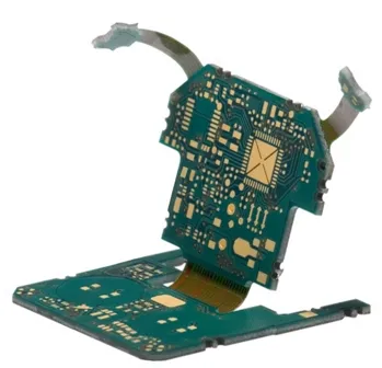
设计刚柔结合PCB

Applies to Altium Designer versions: 23 and 24

There are two rigid-flex design modes available in Altium's PCB design software. The original, or standard mode, referred to as Rigid-Flex, supports simple rigid-flex designs. If your design has more complex rigid-flex requirements, such as overlapping flex regions, then you need the Advanced Rigid-Flex mode (also known as rigid-flex 2.0). As well as overlapping flex regions, the Advanced mode also brings: visual definition of the substacks, easier definition of the rigid and flexible board regions, bends on nested cutouts, custom-shaped splits, and support for bookbinder-type structures. The required mode is selected in the Layer Stack Manager, more on this below.

What is Rigid-Flex?

As the name suggests, a flexible printed circuit is a pattern of conductors printed onto a flexible insulating film. Rigid-flex is the name given to a printed circuit that is a combination of both flexible circuit(s) and rigid circuit(s), as shown in the image.

Flexible circuit technology was initially developed for the space program to save space and weight. It is popular today as it not only saves space and weight - making it ideal for portable devices such as mobile phones and tablets - it can also reduce packaging complexity, improve product reliability, and reduce cost.

Flexible circuits are normally divided into two usage classes: static flexible circuits, and dynamic flexible circuits. Static flexible circuits (also referred to as use A), are those that undergo minimal flexing during assembly and service. Dynamic flexible circuits (also referred to as use B), are those that are designed for frequent flexing, such as a disk drive head, a printer head, or as part of the hinge in a laptop screen. This distinction is important as it affects both the material selection and the construction methodology. There are a number of layer stackup configurations that can be fabricated as rigid-flex, each with its own electrical, physical, and cost advantages.

Mechanical Rigid-Flex Design

Designing a flex or rigid-flex circuit is very much an electromechanical process. Designing any PCB is a three-dimensional design process, but for a flex or rigid-flex design, the three-dimensional requirements are much more important. Why? Because the rigid-flex board may attach to multiple surfaces within the product enclosure, with the attaching and folding process often happening during product assembly. Delivering a working electromechanical design requires close and constant collaboration between the mechanical and electrical engineering teams. The traditional approach to confirm that the folded board fits within its enclosure has been to create a mechanical mockup - known as a paper doll cut out. By its very nature, it's difficult to achieve the accuracy and realism required with this approach.

A board with two rigid regions connected by a flexible region in the ECAD PCB editor and in MCAD.A board with two rigid regions connected by a flexible region in the ECAD PCB editor and in MCAD.

Altium is helping to solve this challenge with CoDesigner, a sophisticated mechanical-to-electronic design interface technology. CoDesigner allows the engineers to pass the board shape and component changes back and forth between the ECAD and MCAD design domains directly from within the ECAD and MCAD design software.

  • Altium Designer also supports including rigid-flex boards as part of a multi-board design. Learn more about Designing Systems with Multiple Boards.
  • For an engaging discussion on the materials, technologies, and processes, as well as the challenges involved with the production of a rigid-flex board, download and read the free Rigid-Flex Guidebook.

Designing a Rigid-Flex PCB

A printed circuit board is designed as a series of layers stacked on top of one another. For a traditional rigid printed circuit board, the board shape defines the board in the X-Y plane, and the stack of layers defines the board in the Z plane. The X-Y board shape is defined in the main PCB editing window, and the layers are configured in the Layer Stack Manager. In a rigid-flex PCB, there is more than one zone or Region in the finished printed circuit board, and each of those Regions can use a different set of layers.

To design a rigid-flex board, you need to:

  • Enable the required Rigid-Flex mode (Layer Stack Manager, Tools » Features » Rigid-Flex, or Tools » Features » Rigid-Flex (Advanced) command)
  • Define the Substack needed for each Region of the board, and configure how those Substacks align with each other in the Z plane.
  • Define the shape of each rigid and flex Region in the X-Y plane, and assign the correct Substack to each Region.

Enabling Rigid-Flex Design

To support the complex structures present in a modern rigid-flex printed circuit board, the Z plane editor - the Layer Stack Manager, provides different display modes for editing the structure of your board. Select the Design » Layer Stack Manager command to open the Layer Stack Manager, where you can enable the required rigid-flex mode, and create and align the Substacks needed in your rigid-flex design.

When the Layer Stack Manager opens, it will show the current board layer Stackup. For a new PCB, this will be a simple two-layer board. To enable the features needed to design a rigid-flex board, open the Tools » Features sub-menu or click the Features button ( ) to select either the Rigid-Flex command, or the Rigid-Flex (Advanced) command.

Select the command to enable the required rigid-flex mode.Select the command to enable the required rigid-flex mode.

When trying to disable the advanced rigid-flex mode or switch to the standard rigid-flex mode for a PCB that already uses advanced rigid-flex features, the warning dialog will open for confirmation.

A quick way to check which rigid-flex mode is being used for a board is to switch to Board Planning Mode (1 shortcut) and have a look at the Active Bar.

  • Standard rigid-flex Board Planning mode Active Bar 
  • Advanced rigid-flex Board Planning mode Active Bar 

To learn about defining the substacks, refer to the following pages:

Working with Board Regions

A Board Region is the term used to describe each user-defined area of the board that needs a unique layer stack assigned to it - a standard requirement for a rigid-flex PCB. In the image below the board shape has been divided into three distinct Board Regions: the upper circular region, the thin center strip, and the lower circular region.

A rigid-flex board viewed in Board Planning Mode, note the board shape has been divided into three distinct Board Regions, each showing its region name and the layer stack assigned to it.

When a new board is created, it defaults to having a single Board Region. If the board design requires multiple regions, then you can either:

  • slice a single Board Region into multiple regions (standard Rigid-Flex mode or Advanced Rigid-Flex mode), or
  • place multiple Board Regions to build up the overall shape (Advanced Rigid-Flex mode).

Board Regions are defined and edited in Board Planning Mode (View menu).

The View menu has three PCB editor working modes with easy-to-remember shortcuts, allowing you to quickly switch between:

  • Board Planning Mode (1)
  • 2D Layout Mode (2)
  • 3D Layout Mode (3)

The default behavior when switching between 2D and 3D view modes is to retain separate zoom and orientation settings for each view mode. If you want to see the same location and orientation of the board as you switch, press Ctrl+Alt+2 or Ctrl+Alt+3, instead of 2 or 3.

To learn about working with board regions, refer to the following pages:

Working with Bending Lines

Bend Lines are defined and edited in Board Planning Mode (View menu).

To learn about working with bending lines, refer to the following pages:

The Properties of a Bending Line

Bending Lines have the following inter-related properties:

  • Bend Angle (a) - the angle the surface of the Flex region is to bend.
  • Radius (r) - the distance away from the bend surface that the bending center-point is located.
  • Width (w) - the width of surface area that will be bent for the given Radius and Bend Angle.

The relationship between the Bend Angle, Radius and width can be expressed as:

  • w = a/360 * 2*Pi*r
  • or in words, width = Fraction of the circumference being bent * Circumference

Browsing Layer Stack Regions and Bending Lines

In the PCB panel’s Layer Stack Regions mode, its three main regions change to reflect the following (in order from the top):

  • The names of the available Layer Stacks.
  • The Stackup Regions defined on the board, or those assigned to a selected Layer Stack.
  • The list of Bending Lines in the selected Stackup Region

While using the Layer Stack Regions mode of the PCB panel, change to the Board Planning Mode view through the View » Board Planning Mode menu, or use the 1 shortcut.

A board can split into distinct regions (Stackup Regions) that are assigned specific layer stackup arrangements (Layer Stacks). Folding areas (Bending Lines) are defined in the board's flexible regions.

When a particular layer stackup name is selected in the Layer Stacks area of the PCB panel, filtering will be applied using the Layer Stack as the scope of the filter. Any board regions assigned to that stackup will therefore be listed in the panel's Stackup Regions area. In turn, any bending lines defined in a selected Stackup Region will be listed in the Bending Lines list area.

Double-clicking on a Stackup Region in the list (or double-clicking on the board region itself in the design space) opens the Board Region dialog (Standard Rigid-Flex mode) or Board Region mode of the Properties panel (Advanced Rigid-Flex mode). Use this dialog/panel to rename a region, assign it to a layer stack, or lock its 3D properties.

Double-clicking on a Bending Line in the panel's Bending Line area list opens the Bending Line dialog in which the line's properties can be edited in detail.

Displaying and Folding a Rigid-Flex Design in 3D

The PCB editor includes a powerful 3D rendering engine, which allows the presentation of a highly realistic three-dimensional representation of the loaded circuit board. This engine also supports rigid-flex circuits, and when used in combination with the Fold State slider in the PCB panel, it allows the designer to examine their rigid-flex design in the flat state (no Bending Line settings applied), the fully folded state (all Bending Line settings applied), and anywhere in between.

To switch to the 3D display mode, press the 3 shortcut key (press 2 to return to 2D or 1 to return to Board Planning Mode). The board will be displayed in 3D. If the component footprints include 3D body objects that define the mounted component, these will also be displayed. In the image below, you can see that the board includes a battery and a battery clip.

To apply all of the Bending Lines, slide the Fold State slider in the PCB panel when set to Layer Stack Regions mode as highlighted in the image below. Note that the bends are applied in the order defined by their sequence number. Bending Lines can share the same sequence number; it simply means that those bends will be folded at the same time when the Fold State slider is used. The board can also be folded/unfolded by running the View » Fold/Unfold command (or by pressing the 5 shortcut).

To be able to interrogate the folding of your board in greater detail, with the ability to effectively fold in slow-motion and pause folding, use the Fold State slider control, located beneath the Bending Lines region of the PCB panel, when configured in Layer Stack Regions mode. Note that one board region must have its Lock 3D Position option enabled (in the Stackup Regions region of the panel). This option can also be enabled in the Board Region dialog, where it is presented as the 3D Locked option. This is required to define the physical ground reference for the 3D display mode (where Z = 0). If this is not done, bends will not be applied when you move the Fold State slider.

Use the Fold State slider (or the 5 shortcut key) to apply all Bending Lines in the order defined by their sequence value (Fold Index).

3D Movie Maker Support for Rigid-Flex Designs

The ability to fold a rigid-flex design can also be captured as a 3D movie. It is very simple to do and does not require the use of movie key frames during the folding sequence.

Refer to the Preparing a 3D PCB Video page for a detailed description of how to make a 3D movie. As a basic guide:

  1. Switch the PCB editor to 3D mode.
  2. Open the PCB 3D Movie Editor panel and create a new video by clicking the New button. Click the newly-created video in the Movie Title region then give it a suitable name.
  3. Create an initial Key Frame showing the board in its unfolded state.
  4. Slide the Fold State slider to show the rigid-flex design in its folded state, then position the folded board as required.
  5. Now create a second Key Frame for this view and set the time. Consider how long you want it to take to fold the rigid-flex design (the Duration setting); typically this would be a few seconds.
  6. To check that the video captures the folding process correctly, click the play button (located in the player controls at the bottom of the panel.

  7. To generate a movie file, add a PCB 3D Video Documentation Output in an Output Job file. Remember to configure the video format options in the Video settings dialog.
  8. Click the Generate Content link in the Output Job file to create the movie file.

The video below was created using this process. It has the two key frames described above, plus one additional key frame that was added at the end to hold the final position for a second.

A simple 3D movie created from three key frames; the folding behavior is defined by the Bending Line Sequence values.A simple 3D movie created from three key frames; the folding behavior is defined by the Bending Line Sequence values.

Learn more about Preparing a 3D PCB Video

Design Considerations

Below is a summary of key design areas that must be considered when designing a rigid-flex PCB:

  • Conductor routing - choice of corner style for routes traveling over a flex region is important; avoid sharp corners; use a curve for least stress.
  • Pad shape and area - use fillets (teardrops) with rabbit ears (anchoring spurs) for single-sided flex. The objective is to capture some of the pad shape with the coverlayer.
  • Through holes - try to avoid through holes in the bend area, particularly in a dynamic application.
  • Coverlayer - avoid stress risers (exposing the incoming track); reduce opening in coverlayer to 250um.
  • Planes - crosshatched, if possible.
  • Staggered lengths - to avoid layer buckling when flexed (bookbinding), stagger the layer lengths by approx 1.5 times the layer's thickness.
  • Service loop - make the flex region slightly longer to help with assembly/disassembly and to allow for product dimensional variations (the extra length is referred to as the service loop).
  • Conserve copper - consider how the flex circuit will be panelized; it might be better to adjust the design to ensure best material usage.
  • Panelization - orient the flex regions to suit the grain of material (bend along the grain).
  • Tear resistance - curved corners; drilled hole at corner; hole in slit; leave metal in corners.
  • Routing - stagger the routes on two layer boards to avoid I beaming, and widen the routes through the bending zone (this is especially important for permanent bends).
  • Static Bend Ratio - setting the ratio of the bend radius to the circuit thickness. Ideally, multi-layer circuits should have a bend ratio of at least 15:1. For double-sided circuits, the minimum ratio should be at least 10:1. For single-layer circuits, the minimum ratio should also be at least 5:1. For a dynamic application, aim for a bend ratio of 20-40:1.
  • Rolled annealed copper is more ductile; plated copper is not the best choice for flexible regions.

Documentation and Drawing Requirements

Typical suggested documentation requirements include:

  1. The Flex PCB shall be fabricated to IPC-6013, class (your requirement here) standards.
  2. The Flex PCB shall be constructed to meet a minimum flammability rating of V-0 (if required).
  3. The Flex PCB shall be RoHS compliant (if required).
  4. The rigid material shall be GFN per IPC-4101/24 (if using epoxy material).
  5. The rigid material shall be GIN per IPC-4101/40 (if using polyimide material).
  6. The flexible copper clad material shall be IPC 4204/11 (flexible adhesive-less copper clad dielectric material).
  7. The covercoat material shall be per IPC 4203/1.
  8. The maximum board thickness shall not exceed (your requirement here) and applies after all lamination and plating processes. This is measured over finished plated surfaces.
  9. The thickness of acrylic adhesive through the rigid portion of the panel shall not exceed 10% of the overall construction. See comments on this above.
  10. Pouch material can be used for ease of manufacturing and must be removed from the flexible portion of the board prior to shipping.
  11. The flexible section thickness shall be (your requirement here). Do not add this note if this thickness is not critical.
  12. Minimum copper wall thickness of plated through holes to be (your requirement here; .001” average is recommended) with a minimum annular ring of (your requirement here; 002 is recommended).
  13. Apply green LPI soldermask (if required) over bare copper on both sides in the rigid sections only of the board. All exposed metal will be (specify your surface finish requirement here).
  14. Silkscreen both sides of the board (if required) using white or yellow (most common) non-conductive epoxy ink.
  15. Marking and identification requirements.
  16. Electrical test requirements.
  17. Packaging and shipping requirements.
  18. Impedance requirements.

Additional Drawing Detail

  1. A drill table detailing finished hole size, associated tolerances and plated/not plated.
  2. A dimensional drawing, including reference datum(s), critical dimensions, rigid to flex interfaces, bend location and direction markers.
  3. Panelization detail, if required.
  4. Construction and Layer detail, detailing material used for each layer, thicknesses and copper weights.

References

Flex and Rigid-Flex Circuits Technical Engineering Guide - Epec Engineering Technologies

Flexible Circuit Technology - Joe Fjelstad

Flex Circuits Design Guide - Minco Products Inc

Minco Products Flex Resources

Machine Design website:

可用的功能取决于您的 Altium Designer 软件订阅级别

Content