
Importing a Design from Allegro
To support the need to load and work with Cadence® Allegro™ Design files, Altium Designer’s Import Wizard includes the capability to import Allegro PCB designs in binary (*.brd - check the import prerequisites), ASCII (*.alg) forms (which are translated to Altium Designer PCB files (*.PcbDoc)), and Allegro footprint files (*.dra) (which are translated into Altium Designer PCB library files (*.PcbLib).
The Allegro PCB files (up to version 17.4) are translated to Altium Designer PCB files by the Wizard’s Allegro importer, which is included as an Altium Designer platform extension.
Import Prerequisites
The Altium Designer Import Wizard can directly import Allegro ASCII format PCB files (*.alg). To import a binary Allegro PCB (*.brd) or footprint (*.dra) file, the file must be translated from binary to ASCII. The binary-to-ASCII translation is performed by the Cadence utility called Extracta, a configurable command-line utility that is capable of extracting and translating data from the binary PCB file, with the extraction process controlled by a Command file that details the data required to be extracted. Learn more about Extracta.
Supported Binary File Versions
Extracta will only extract data from Allegro binary PCB (*.brd) and footprint (*.dra) files whose version is the same as, or lower, than the version of Extracta being used. To check the version of Extracta, open a Windows Command prompt and enter Extracta -version.
Importing When Allegro is On the Same PC as Altium Designer
If Altium Designer is installed on the same PC as Cadence Allegro, the extraction process can be handled automatically by the Altium Designer Import Wizard. The process of running the Wizard is outlined below. Note that the Wizard also performs file version checking, Allegro files up to 17.4 are currently supported by the Wizard.
Importing When Allegro is Not on the Same PC as Altium Designer
If Extracta.exe is not installed on the same PC as Altium Designer, you can manually run the extraction process on the PC where the Extracta utility is installed. Altium Designer runs the extraction process using the Allegro2Altium.bat file.
To manually extract the ASCII board data:
-
Copy the
Allegro2Altium.batfile from the<Altium_Designer_Installation_Folder>\Systemfolder to a known location on the PC that has Allegro installed. -
Copy the Allegro binary (
*.brdor*.dra) file that you want to convert, into the same folder. -
Launch a Windows Command Prompt and use the
cdcommand to get into the folder that contains the copied files. Example:cd C:\Documents\Files\Test -
Once in the right directory, run the Altium batch file using the
Allegro2Altiumcommand. For example:Allegro2Altium your_file.brdor
Allegro2Altium your_file.drawhere
your_file.brdoryour_file.drais the name of the binary file you want to convert. Surround the filename with double quotes if the filename contains spaces, for exampleAllegro2Altium "your file.brd". -
The process will create an ASCII file (
your_file.brd.algoryour_file.dra.alg) in the folder. Copy this ASCII board file back to the PC where it can be imported into Altium Designer using the Import Wizard.
 The ASCII Allegro design conversion process is controlled by the special
 Allegro2Altium batch file.
Accessing and Running the Importer
The Allegro PCB design file importer is available through Altium Designer's Import Wizard (File » Import Wizard), where the option is selected in the wizard's Select Type of Files to Import page – choose the Allegro Design Files option.
When adding files to the import file list, use the file browser's filter drop-down menu to choose between binary (*.brd) or ASCII (*.alg) Allegro files.
.") Select either binary or ASCII Allegro design files for import. Allegro must be installed on the local machine to import binary Allegro files (
Select either binary or ASCII Allegro design files for import. Allegro must be installed on the local machine to import binary Allegro files (*.brd).
If you attempt to import a binary Allegro Design File (*.brd) using the Import Wizard and you do not have Allegro installed locally, the import process is suspended and a warning dialog is displayed. In this case, import an ASCII version of the design file that has been created through the Allegro ASCII file extraction process (as outlined above).

To complete the file import and translation process, follow through the remaining pages of the Import Wizard to customize and finish the conversion of the Allegro Design Files into Altium Designer design files.
Import Wizard - Allegro Design Files
Allegro Design Files

Selecting the Design Files to Import

Click Add to choose which Allegro design files to import. You can delete a selected file by clicking Remove.
Selecting the Constraint Files to Import

Click Add to choose which Allegro *.DCFX constraint files to import. You can delete a selected file by clicking Remove.
Selecting the Footprint Files to Import

Click Add to choose which Allegro footprint files (*.dra) to import. You can delete a selected file by clicking Remove.
Setting the Reporting Options

Use the Reporting Options page to set up general log reporting options. A Log Report in ASCII file format (*.LOG) is generated for each translated Allegro PCB file. This log is saved in the \Imported subfolder of your original Allegro files. Open the Log Report after translation in a text editor to examine the details.
Under General Settings, enable the desired option(s).
Setting PCB Specific Options
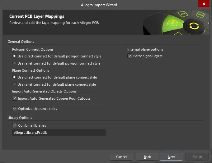
This page of the Wizard is used to specify options specific to the PCB import process.
Select the desired Polygon Connect Options: either Use direct connect for default polygon connect style or Use relief connect for default polygon connect style.
Select the Plane Connect Options: either Use direct connect for default plane connect style or Use relief connect for default plane connect style.
Enable the Import Auto-Generated Copper Pour Cutouts option in the Import Auto-Generated Objects Options region to import the voids that are auto-generated in the Allegro PCB Editor as cutouts when the file is translated.
Enable the Optimize Clearance Rules option to use optimization for the clearance rules.
Enable the Force signal layers option to import plane layers as signal layers.
Editing the Layer Mapping

This page of the Wizard is used to review and edit the layer mapping for each Allegro PCB. Default mapping is provided by the Wizard to build the layer mapping for each PCB. Layer mapping can be customized for each of your designs to be imported. You may wish to import multiple Allegro PCB designs and map the same Allegro layer to the same Altium Designer layer. You can set your layer mapping once and use this layer mapping for all of your files to be imported. The advantage of importing in this manner is that batch layer management can save time when importing multiple designs. The disadvantage to using this is that Default Layer Mapping is not always intelligent with differing structures in designs, and therefore, some manual changes may be required.
The Allegro Layer Name, Allegro Layer Type, Altium Layer Type, and Altium Layer Name are listed in the grid region. Click on the ![]() icon on the right-hand side of each region to filter the displayed list of that region.
icon on the right-hand side of each region to filter the displayed list of that region.
If desired, you can edit the layer mapping for any or all Allegro Import PCB designs or library files on this page of the Wizard. To group by a column, drag the column header into the area at the top of the table specified.
Right-clicking in the grid region provides you with a sub-menu where you can:
- Load Layer Mapping – select to open the Load Configuration dialog to load the desired mapping files.
- Save Layer Mapping – select to open the Choose File to Save Layer Mapping dialog and choose the path in which to save the layer mapping.
Specifying the Output Directory

Use this page of the Wizard to review the output project structure and specify the output directory in which to import the files. Use the Browse Folder icon to search for and choose the Project Output Directory.
Click Menu to access options to edit the project structure:
-
Create Project – click to open the Create Project dialog to add a project.

Use the Create Project dialog to add a new project. -
Rename Project – click to rename the selected project. This option is available only when a
*.PrjPcb fileis selected. - Remove Selected Projects – click to remove the selected project from the PCB Projects structure.
- Reset Structure to Default – click to reset the PCB Projects structure to the defaults.
-
Add Designs to Project – click to add a design(s) to the project. This option is available only when a
*.PrjPcb fileis selected. -
Remove Selected Designs - click to remove the selected design files.
Closing the Wizard

The Allegro Import Wizard has completed. Click Finish to close the Wizard.
Imported Allegro files:
Allegro files translate as follows:
-
Allegro Binary PCB Design files (
*.brd) translate to Altium Designer PCB files (*.PcbDoc). -
Allegro ASCII Extract files (
*.alg) translate to Altium Designer PCB files (*.PcbDoc). -
Allegro footprint files (
*.dra) translate to Altium Designer PCB library files (*.PcbLib).
Notes
-
Check out the detailed Knowledgebase article on importing Allegro files into Altium Designer.
-
In Altium Designer, 3D STEP models are stored inside a 3D Body object, which is placed in the PCB footprint.
-
Learn more about Creating a PCB Footprint in Altium Designer.
-
Learn more about Working with 3D Bodies and Additional Tools for Working with 3D Bodies.
-
-
The Allegro Importer supports importing custom pad stacks defined in an Allegro board design. Import of such a design will create custom pad shapes in Altium Designer. In addition, where thermal tie legs are defined as part of the custom pad stack in Allegro, these will be imported as custom thermal relief connections.
-
When thermal relief of the orthogonal, diagonal, or full contact type is set in the Properties panel for a pad in the Allegro Constraint Manager, these pads are imported into Altium Designer with custom thermal reliefs configured accordingly. Note that if the thermal relief width or gap is not set for a pad in the Allegro Constraint Manager, values for the Conductor Width and Air Gap Width in Altium Designer will be taken from the rules for the minimum line width and pin spacing rule defined in the Allegro design, respectively.
-
In order to provide consistency with the Allegro design, values of width-related rules are imported to Altium Designer as follows:
-
Min Neck Width –> Min Width
-
Line Min Width –> Preferred Width
-
Line Max Width –> Max Width
If a value is absent (or equals zero) in the Allegro design, it inherits the value of the previous range.
-
-
When importing an Allegro design, you can import more detailed pad stack information. This enables importing of more accurate pad properties to Altium Designer, aligning them more closely with their equivalents in the originating Allegro design. As part of this ability, different copper shapes on layers when importing an Allegro footprint file are supported.
-
When importing an Allegro design, if a polygon pour is less than 2500 sq.mil in size, its Remove Islands Less Than option is automatically disabled.
-
When importing an Allegro design, the import of padstack-level solder and paste masks for pads (regular and custom shapes, including tented pads) and vias (involving the calculation of expansions and including tented sides) can be supported.
Also, when importing an Allegro design with the listed below defined sub-classes on Top or Bottom layers, a component layer pair is created in the generated PCB document to accommodate values from these Top and Bottom layers, with these layers hidden by default with respect to their visibility.
Allegro Design Sub-class
Altium Component Layer Pair
Layers - Components - Comp value
COMPONENT_VALUE_TOP and COMPONENT_VALUE_BOTTOM
Layers - Components - Dev type
DEVICE_TYPE_TOP and DEVICE_TYPE_BOTTOM
Layers - Components - Tolerance
TOLERANCE_TOP and TOLERANCE_BOTTOM
Layers - Components - User part
PART_NUMBER_TOP and PART_NUMBER_BOTTOM