
KB: Scale schematic symbols to align on the preferred grid size in one go
Solution Details
It is possible to change the grid size of all schematic symbols in one go parametrically, say, from 2.5mm in metric to Altium standard 100mil. There are two systematic ways of selecting and editing multiple primitives at once:
- right click on a primitive, say a pin, Find Similar Object..., set the scope to have all similar objects selected, in Properties panel, modify the common dimension objects such as X, Y, and Pin Length with a formula 'Round(!*0.0254/2.5)*100' to round 2.5mm to 1mil first and then scale the value to the nearest 100mil, where '!' denotes the current value to be overwritten.
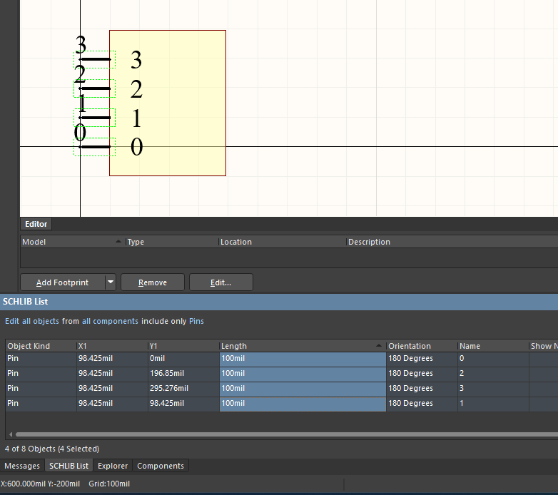
- open SCH/SCHLib List panel, set the mode at the top in blue texts, say, 'Edit all objects from all components include only Pins', shift-select along a column such as X1, Y1, and Length, left-click on a cell along the column to type a formula 'Round(!*0.0254/2.5)*100' to round 2.5mm to 1mil first and then scale the value to the nearest 100mil, where '!' denotes the current value to be overwritten.
Batch Edit through Find Similar Object:
1 If not already, View » Toggle Units to make sure you are in Imperial 100mil grid.
2 Select a primitive such as a pin, right-click and Find Similar Object.

3 Set the scope to select all objects subject to batch edit with common attributes.

4 In Properties panel, modify the value of dimension attributes by typing a formula 'Round(!*0.0254/2.5)*100' to round 2.5mm to 1mil first and then scale the value to the nearest 100mil, where '!' denotes the current value to be overwritten. 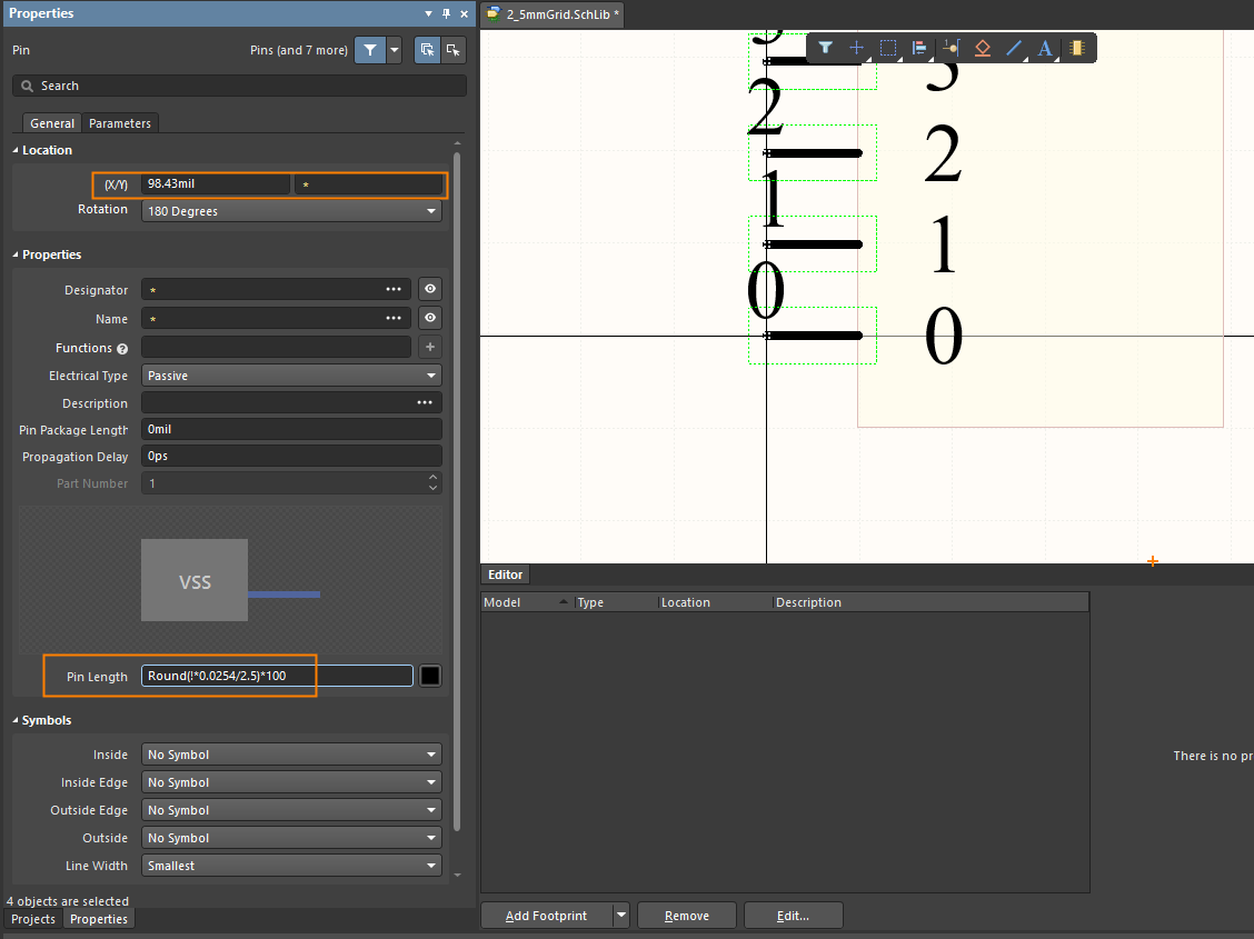
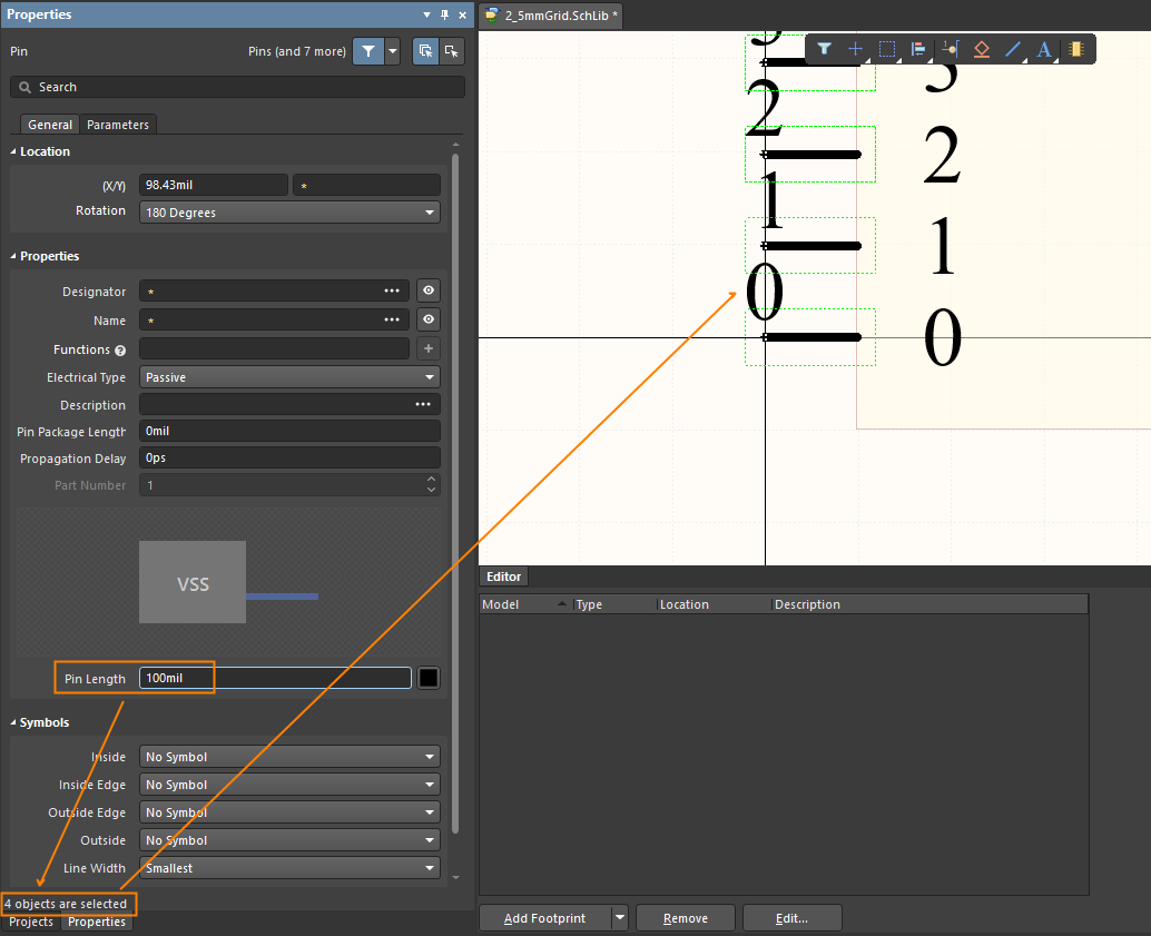
5 Hit Enter to confirm the value updated for all objects selected.
Batch Edit in SCH List/SCHLib panel:
1 If not already, View » Toggle Units to make sure you are in Imperial 100mil grid.
2 In SCH List panel (if in *.schdoc) or SCHLib List panel (if in *.schlib), set the mode/scope in blue text at the top to list all objects of interest. e.g. 'Edit all objects from all components include only Pins' 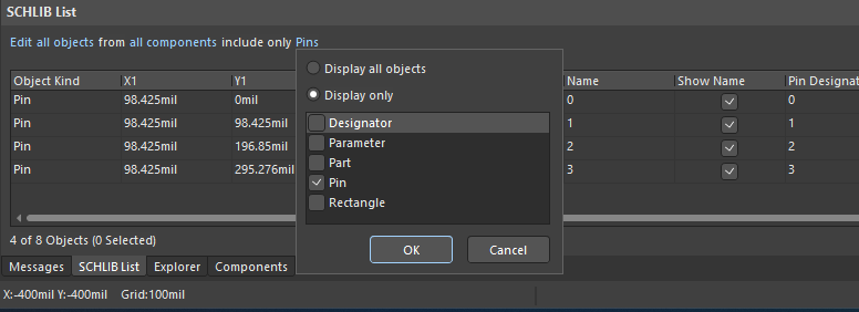
3 Shift-select along a column such as X1, Y1, and Length attributes related to dimensions.
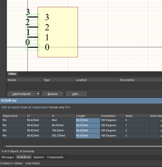
4 Left-click on one of cells along the column while still holding down Shift, and type a formula 'Round(!*0.0254/2.5)*100' to round 2.5mm to 1mil first and then scale the value to the nearest 100mil, where '!' denotes the current value to be overwritten. 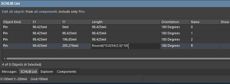
5 Hit 'Enter' to confirm all cells of the column selected in the step 3 overwritten by the new value
It goes without saying that numerical values used in the above is for an illustrative purpose that the technique can be apply to scale symbol primitives from any grid size to another. Specifically, the above formula can be expressed more generally as Round(!*<conversion_factor>/<source_grid_size>)*<target_grid_size>, where:
• <conversion_factor> is 0.0254 if converting from mm to mil and 39.37 if converting from mil to mm
• <source_grid_size> is the grid size in the source grid unit to be scaled and aligned
• <target_grid_size> is the grid size in the target grid unit to which a primitive should be scaled and aligned
Further reference Using Find Similar Objects Tools
Further reference on SCH/SCHLib List panel: List Panels
Further reference ROUND
Further reference Modification Using an Expression