
KB: Short two different nets intentionally
Solution Details
At large, these are ways two different nets can be ohmically shorted together in a design without causing any violation:
1 create Net Tie Component
2 use Signal Harness
3 place a 0-ohm resistor component explicitly
Net Tie Component to short two different nets:
In order to short two different Nets in the design, the primary approach is to create a Net Tie Component.
1 With *.pcblib opened, place two pads in a footprint
2 Short them with a Copper Region in between.
3 Make sure that the copper Region just extends to the sides of the pad but not to the snap point in the middle of the pad itself. Otherwise, connecting tracks and polygons won't connect to the snap point of the pads later in the design.

On the other hand, if you encounter the error message Net Tie failed verification: [...] has isolated copper later in a design with the component placed during DRC verification, then it is likely that the shorting copper in between the two pads is too small. Either that, or you have some other floating pads/vias in the footprint without the shorting copper.
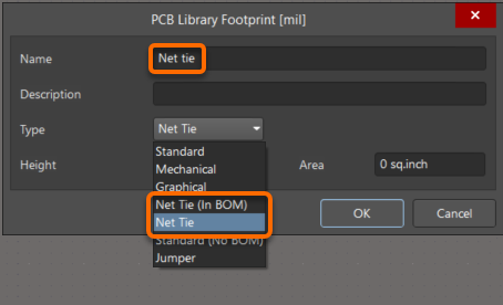
4 Tools » Footprint Properties to give it a Name and to set the Footprint Type to one of the Net Tie options.
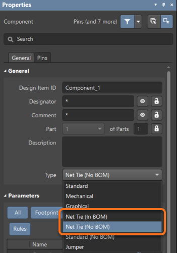
5 create a corresponding schematic symbol in a *.schlib and use the Properties panel to set the symbol Type to one of the Net Tie options
6 add the footprint in created in steps 1-4 to the schematic library symbol in step 5: Schematic Libraries
Specific instructions on how to construct a planer inductor shape:
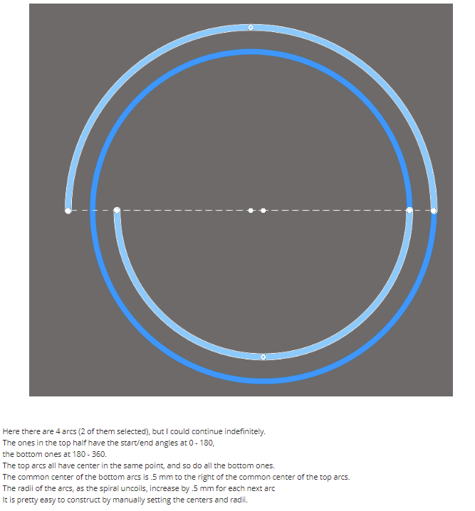
Planer inductor, coil, spiral antenna pattern can be constructed by placing and connecting 180deg arc primitives of incrementally changing radius. The end result is a long contiguous copper piece where its two ends are terminated by pads to be registered as a Net Tie Component.
Below illustrate a visual example of how multiple arcs are placed together to form a spiral pattern.
For further information on Net Tie Component:
Using Net Ties to Meet PCB Design Requirements
Intentionally Connecting Two Nets
Connecting Two Nets with a Net Tie Component
Use of Signal Harness to short two different nets:
In a slightly different context where you do NOT want to introduce/place additional footprint by way of a Net Tie Component, another technique/hack to short two different nets would be to make use of signal harness, which becomes particularly handy, for example, when connecting nets across many repeated multi-channel block in daisy-chain.
Explicitly placing a zero-ohm resistor component:
If the net connection may need to be broken frequently, say for a debug purpose, you may find populating an explicit zero-ohm resistor component more convenient instead.