
KB: Define single layer stackup
Created: March 30, 2023 | Updated: March 08, 2024
Starting in version: 18
Up to Current
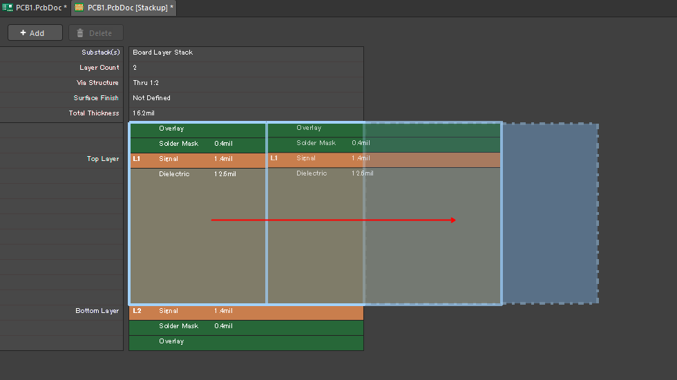
[Why] Define a single layer board such as of a single-sided flex cable. [What] In the Layer Stack Manager, excessive copper layer cannot be deleted. [How] Invoke Design » Layer Stack Manager and Tools » Features » Rigid/Flex (Advanced), shift-select layers from the top down to the core dielectric (not including bottom copper layer), drag them to right to introduce another substack, and back in the main pcb editor, assign this substack in Board Planning Mode (keyboard shortcut '1') to the board region.
Solution Details
The Altium Layer stack manager does not currently allow for removal of top or bottom layer due to a limitation with drill pairs where at least two layers are assumed to exist. In early versions of AD21 it was possible to remove the bottom layer, but this was not a supported feature and caused some unwanted issues in other functions of Altium Designer. To fix those issues, in AD21.3, the ability to remove the bottom layer had been disabled again.To create a single-sided/one layer PCB within current versions of Altium Designer, you need to make sure the copper is all on the desired side of the PCB (everything on the top layer...or everything on the bottom layer). Then check with your fab house to see how they prefer to receive information on single layer PCBs. Rather than providing them with the full set of Gerber files, you generally only need to plot the layers they want, to produce this PCB. Make sure your through hole pads remain as through hole pads, as you will need the drill information.
Preparing Fabrication Data in Altium Designer | Altium Designer 23 User Manual | Documentation
In two layer stackup, set the thickness as 0 mm for the second layer. Put a note for the fabricator to not create this 0mm layer. The layers themselves will always have at least a top and bottom layer in the layer stackup but the setup can be done as suggested above with detailed fab notes as required by your fabricator.
In the layer stack manager, remove the 'stack symmetry' option. Under Tools ► Material Library, you can create a new foil material and call it 'Aluminum' for example. Then you can select the bottom layer and change the material to your custom material type.
In the PCB, under Design ► Rules ► Routing ► Routing Layers, disable the bottom layer for routing.
In case of flex-only one-layer stack, the most streamlined method would be to set the stackup in Advanced Rigid-Flex mode and to introduce a substack to be assigned to your sole board region:
https://www.altium.com/documentation/altium-designer/designing-rigid-flex-pcb#!designing-a-flex-only-pcb-advanced-mode
Invoke Design » Layer Stack Manager and Tools » Features » Rigid/Flex (Advanced), shift-select layers from the top down to the core dielectric (not including the second bottom copper layer), drag them to right to introduce another substack, and back in the main pcb editor, assign this substack in Board Planning Mode (keyboard shortcut '1') to the board region.
 There is a caveat here to be noted that flex bending feature will not work predictably without a default main board region, which is to be locked and used as a reference of rotation.
 Another option is to use Printed Electronics feature without any insulating layer between two signal layers, and make the sum of the two layers as one. Here's documentation that may be helpful:
https://www.altium.com/documentation/altium-designer/designing-for-printed-electronics
You may try various suggestions by some users in this feature request (and please kindly upvote to keep the momentum going):
https://bugcrunch.live.altium.com/#/idea/10797
You can also use draftsman to generate the layer stack up, since the stack up in draftsman can be edited and layers can be removed. You may create a Draftsman fabrication drawing with Place ► Layer stack legend then in the Properties panel 'Layer Info' section, uncheck the visible option for layer number 2.
Here is the doc on how to use draftsman:
https://www.altium.com/documentation/altium-designer/streamlining-board-design-documentation-with-draftsman