What’s New in Altium Designer
Explore new features, enhancements, and important changes introduced in the latest version of
Altium Designer, or see what we’re working on now for upcoming releases.
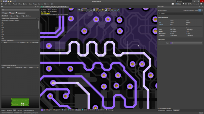
Constraint Manager Improvements
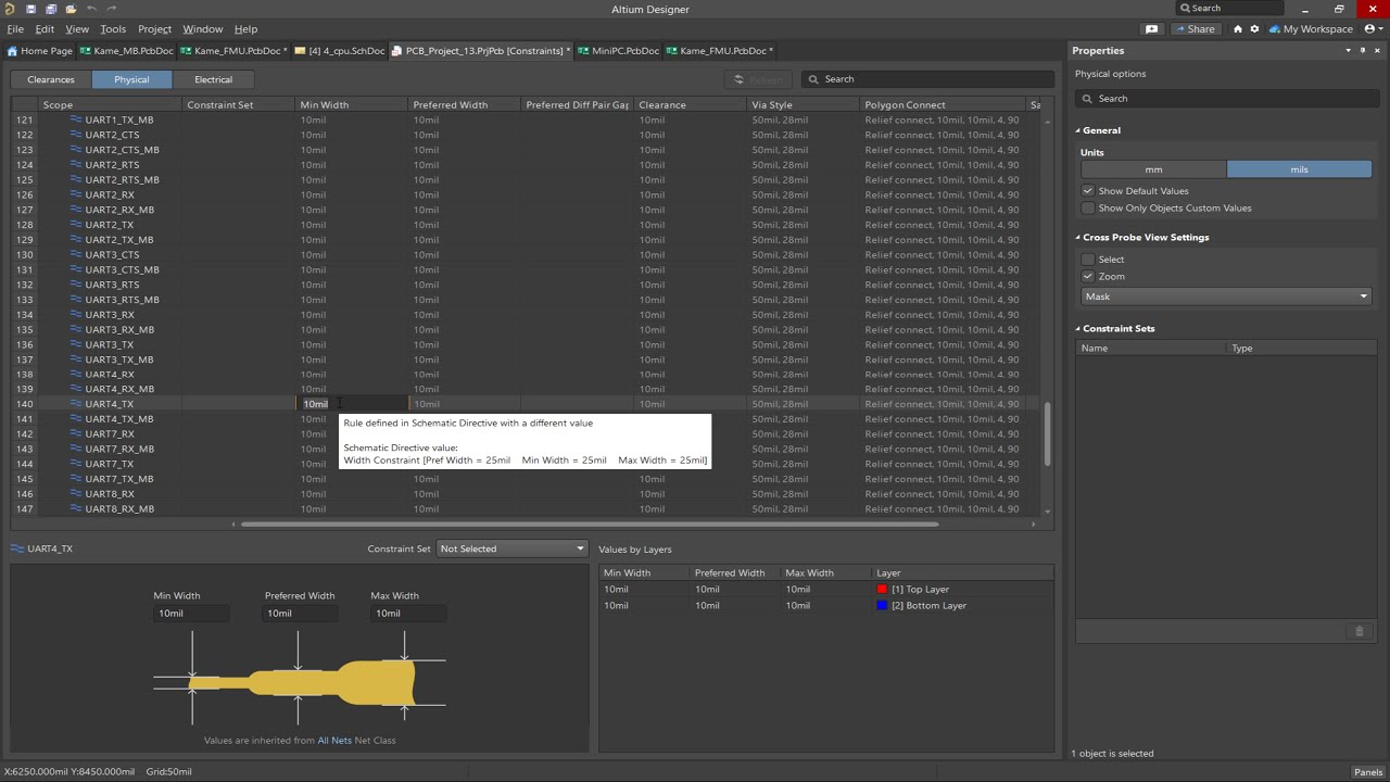
Automatically Propagate Width Values in the Constraint Manager
You can now enter a width value into a single cell at the top grid area, and it will automatically propagate to all corresponding width or gap fields. Furthermore, when working from a schematic, there is an indication of the sync status between constraints defined in the Constraint Manager and those specified through design directives in the source schematics.
RECOMMENDED CONTENT
To see an overview about the Constraint Manager, visit the feature page.
To see the Constraint Manager in action, check out our recent webinar Empowering Faster Electronics Development with Altium Designer 24.
Check out our recent OnTrack Podcast video on the Constraint Manager, Deep Diving Into Altium Designer's New Constraint Manager.
Visit the documentation page to learn about the Constraint Manager.
Discover the latest features and capabilities of Altium Designer 24 with free training.
PCB Layout Enhancements
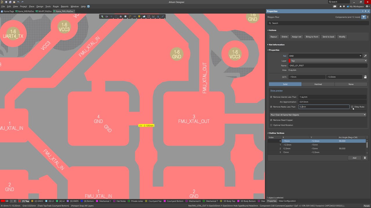
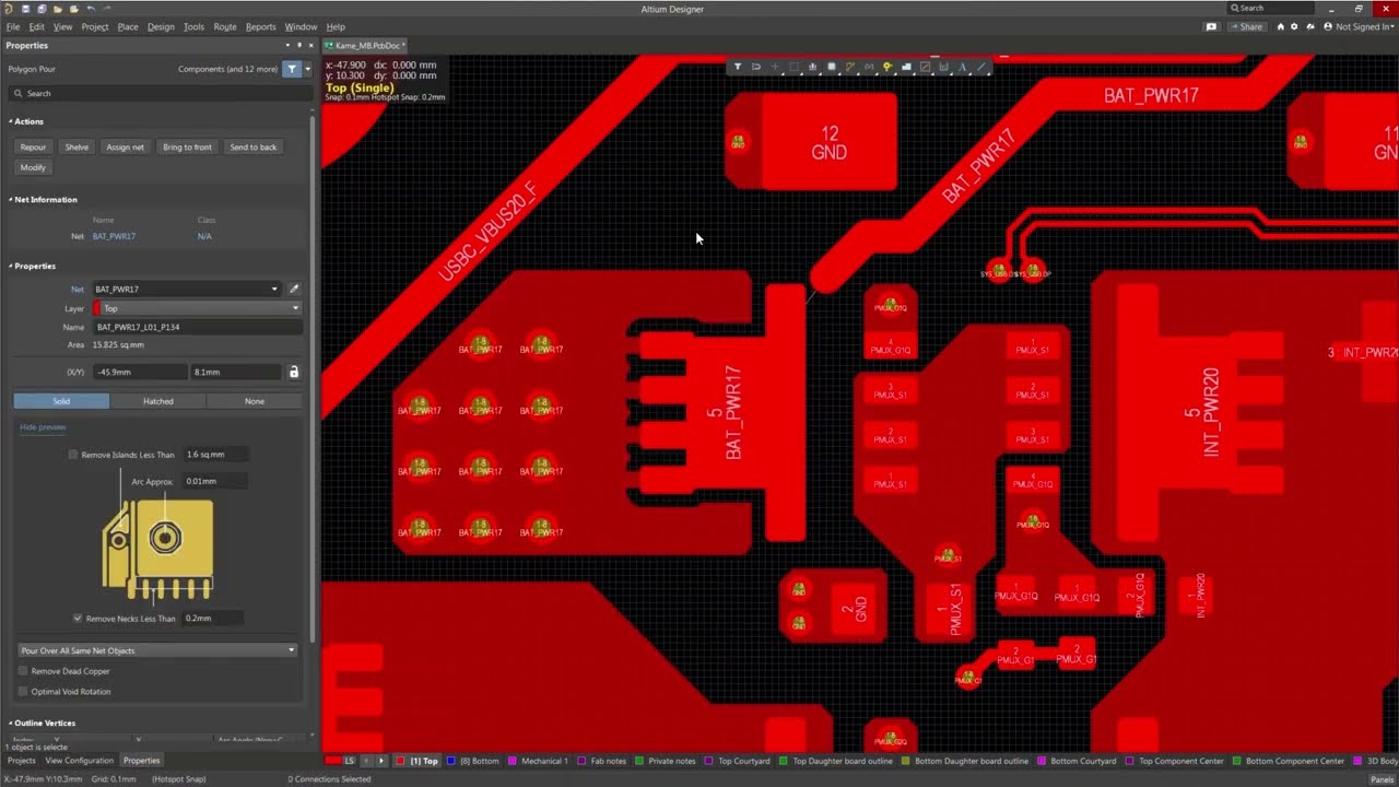
Remove Polygon Necks Less Than a Specified Width
With the new "obey rules" option in the properties panel, you now have the capability to remove necks less than a specified width for placed polygon pours. Furthermore, Altium Designer now observes user-defined geometries for the component selection bounding box when moving a component in Push Obstacles mode.
RECOMMENDED CONTENT
Visit the documentation page to learn about PCB Layout.
Discover the latest features and capabilities of Altium Designer 24 with free training.
Data Management Improvements
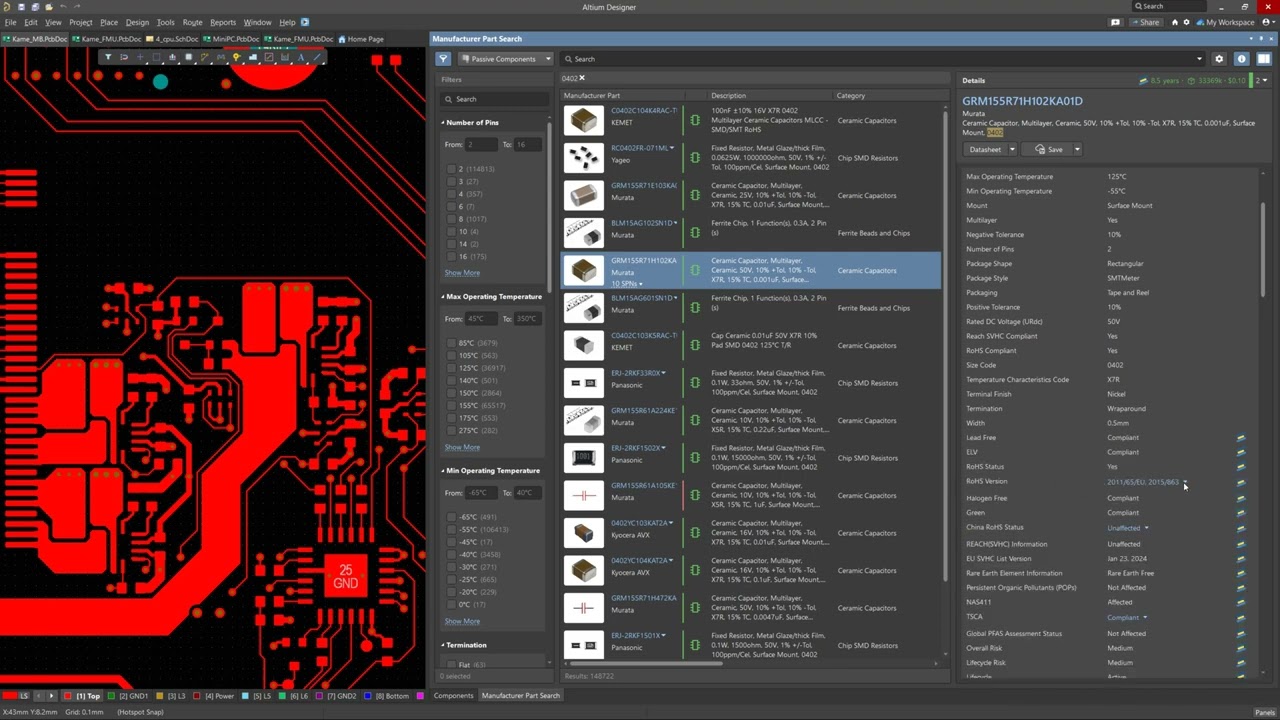
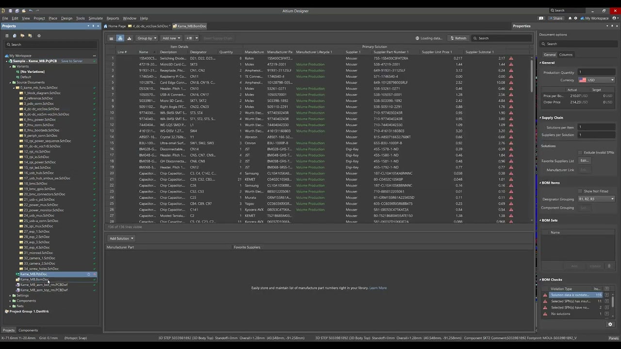
See the Exact YTEOL Value for Your Components
The real value for years to end of life parameter is accurately displayed across all instances where SiliconExpert data is presented, ensuring clarity and precision in your design process. Additionally, we’ve added support for referencing SiliconExpert compliance datasheets, enhancing accessibility and usability. We’ve also included support for the newest Microsoft Access Database file format when synchronizing Database to Workspace components.
RECOMMENDED CONTENT
To see an overview about the Manufacturer Part Search, visit the feature page.
Visit the documentation page to learn about the searching and placing components.
Discover the latest features and capabilities of Altium Designer 24 with free training.
Altium Designer 24
Constraint Manager Improvements
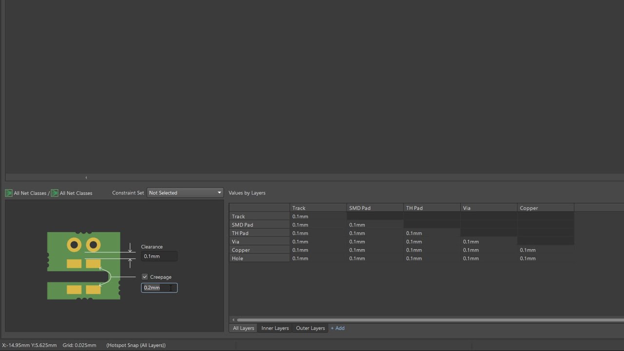
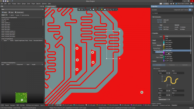
Ensure Accurate Electrical Clearances with the Constraint Manager
A Creepage rule can now be specified for electrical clearances between nets and/or differential pairs, facilitated by the matrix in the Clearances view. Also, support has been added to the clearance matrix for multi-editing within a selected row or column to streamline your workflow.
RECOMMENDED CONTENT
To see an overview about the Constraint Manager, visit the feature page.
To see the Constraint Manager in action, check out our recent webinar Empowering Faster Electronics Development with Altium Designer 24.
Check out our recent OnTrack Podcast video on the Constraint Manager, Deep Diving Into Altium Designer's New Constraint Manager.
Visit the documentation page to learn about the Constraint Manager.
Discover the latest features and capabilities of Altium Designer 24 with free training.
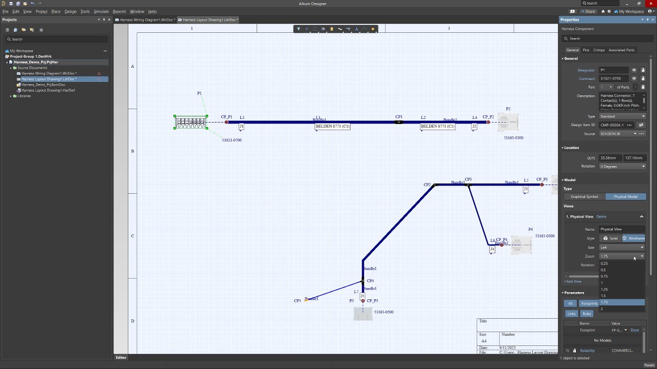
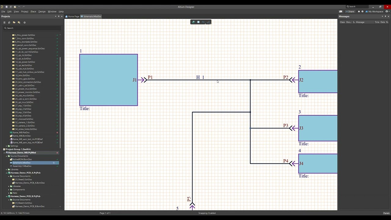
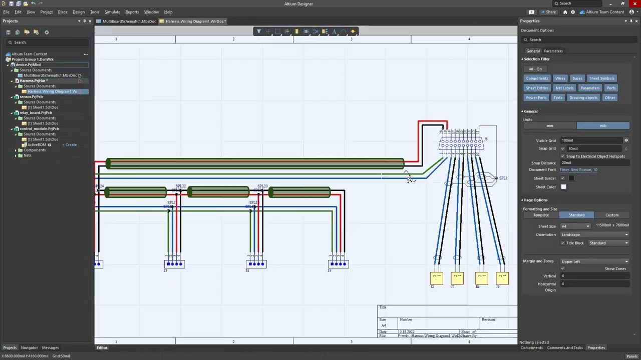
Harness Design Improvements
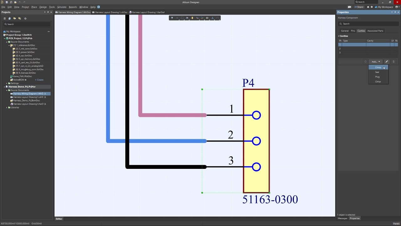
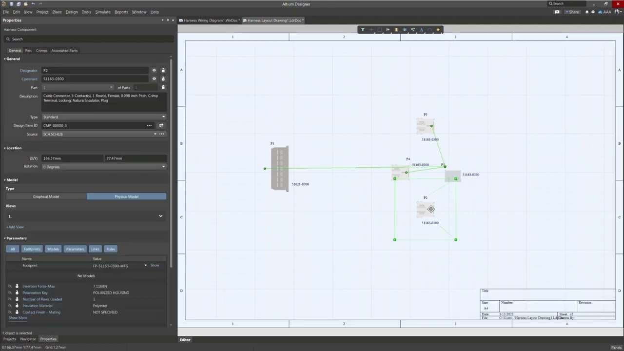
Specify Details for Each Pin of Your Harness Component
You now have the ability to specify crimps, seals, plugs, or other cavity parts for each required pin directly within the Wiring Diagram. These elements are also seamlessly integrated into the wiring list and connection table in the Draftsman document, providing clarity and precision to your designs.
RECOMMENDED CONTENT
To see an overview about Harness Design, visit the feature page.
Visit the documentation page to learn about Harness Design.
Discover the latest features and capabilities of Altium Designer 24 with free training.
Simulation Improvements
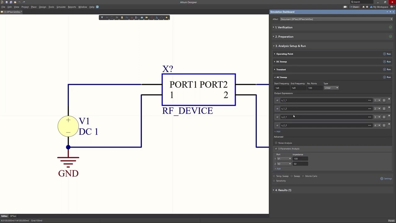
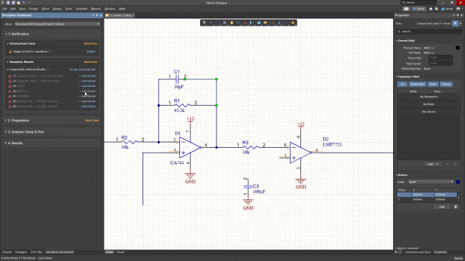
Utilize S-Parameters to Characterize Your Networks
Altium Designer’s S-parameters tool, available within the Simulation Dashboard panel, offers a method to characterize networks by evaluating the ratio of incident and reflected microwaves, effectively addressing challenges in high-frequency circuits.
RECOMMENDED CONTENT
- Witness the benefits of using the Simulation tool in this short video.
- To see an overview about the Simulation tool, visit the feature page.
- Visit the documentation page to learn about the Simulation tool.
- Discover the latest features and capabilities of Altium Designer 24 with free training.
Constraint Manager Enhancements
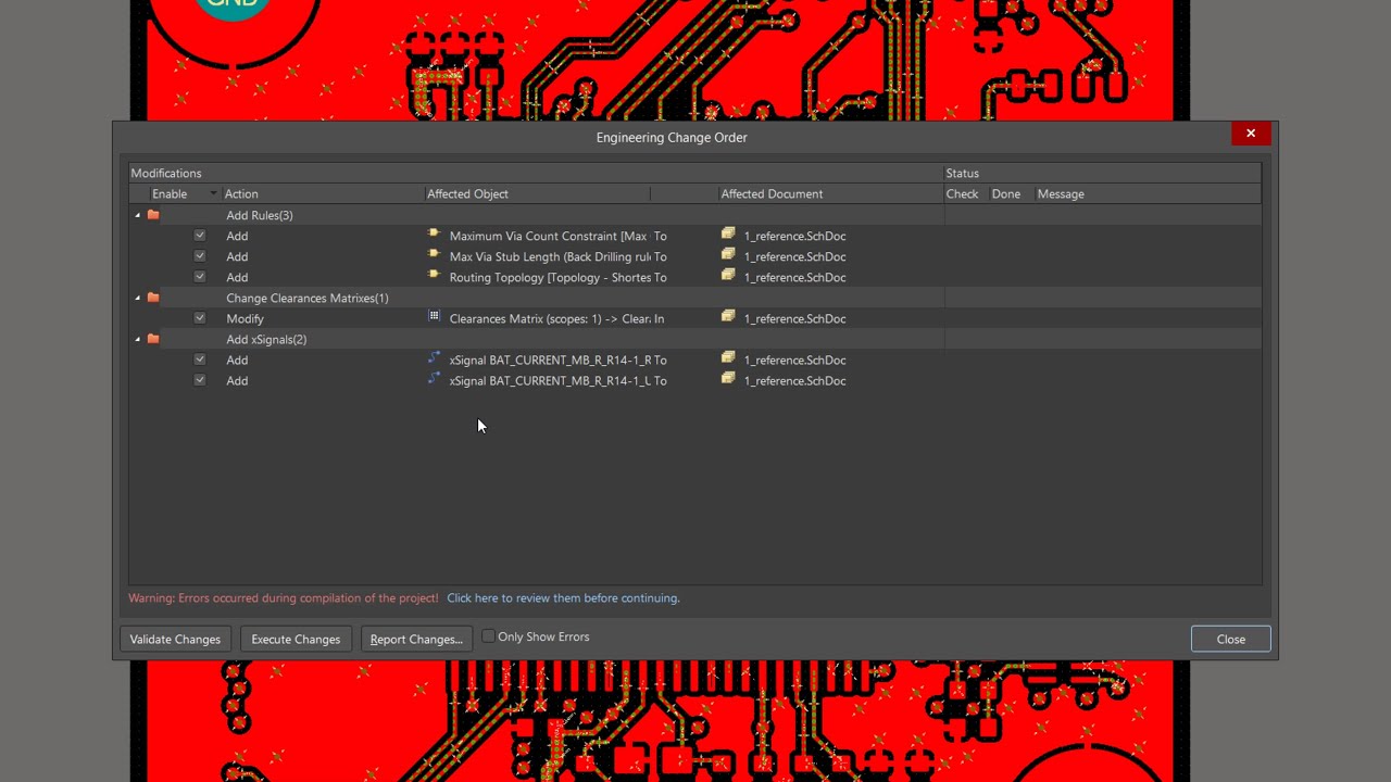
Transfer Design Constraints Between your PCB and Schematic
When accessing the Constraint Manager from the PCB editor and defining constraints on the Physical and Electrical views, it is now possible to transfer those constraints to the Schematic through the Engineering Change Order (ECO) process. This enhancement ensures design consistency by reducing errors and saving time in the constraint definition process.
RECOMMENDED CONTENT
- To see an overview about the Constraint Manager, visit the feature page.
- To see the Constraint Manager in action, check out our recent webinar Empowering Faster Electronics Development with Altium Designer 24.
- Check out our recent OnTrack Podcast video on the Constraint Manager, Deep Diving Into Altium Designer's New Constraint Manager.
- Visit the Constraint Manager documentation page to learn more.
Harness Design Improvements
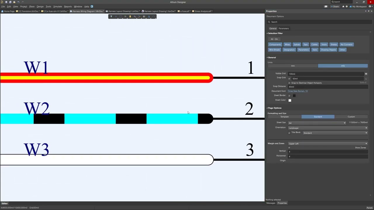
Set Multiple Colors to a Wire in your Harness Design
Altium Designer has added support for multi-colored wires, with the ability to define primary, secondary, tertiary, and border colors as part of a wire's parameters to help expand the functional identification capability of wires in your design.
RECOMMENDED CONTENT
- To see an overview about the Harness Design tool, visit the feature page.
- Check out our recent webinar on Harness Design, Future-Proof your Wire Harnesses with Altium Designer.
- Visit the Harness Design documentation page to learn more.
PCB Layout Replication Improvements
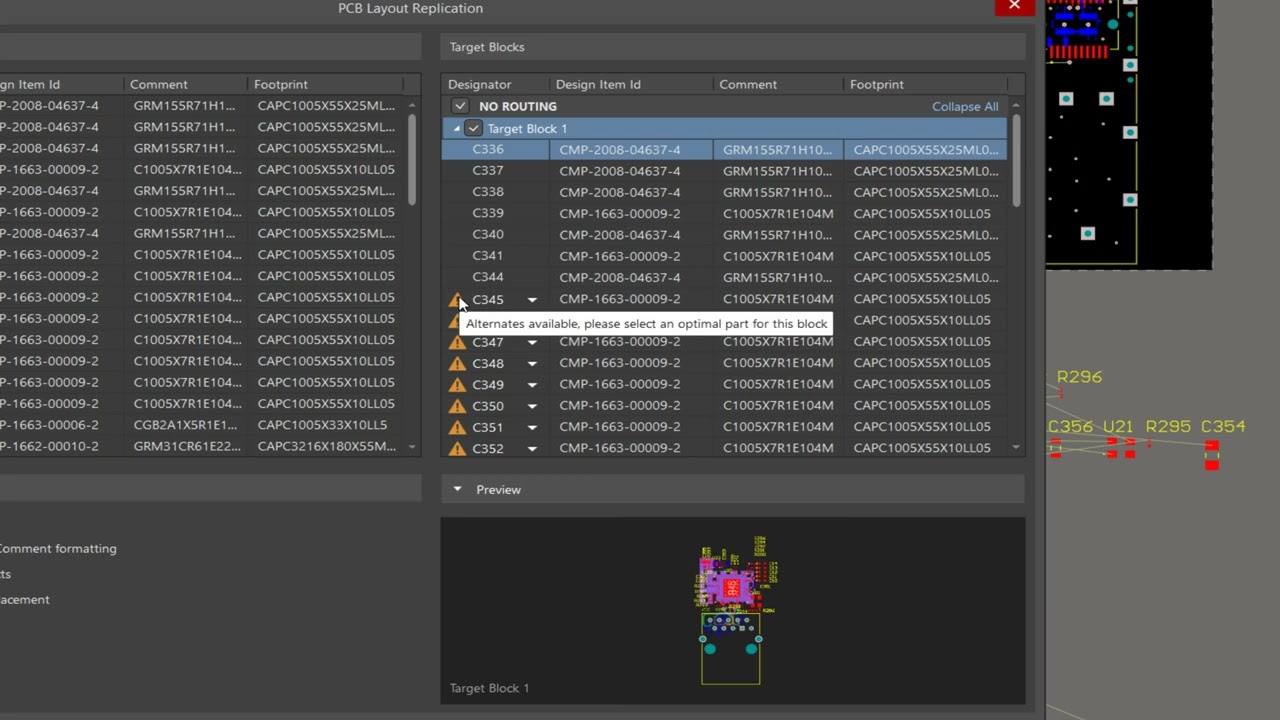
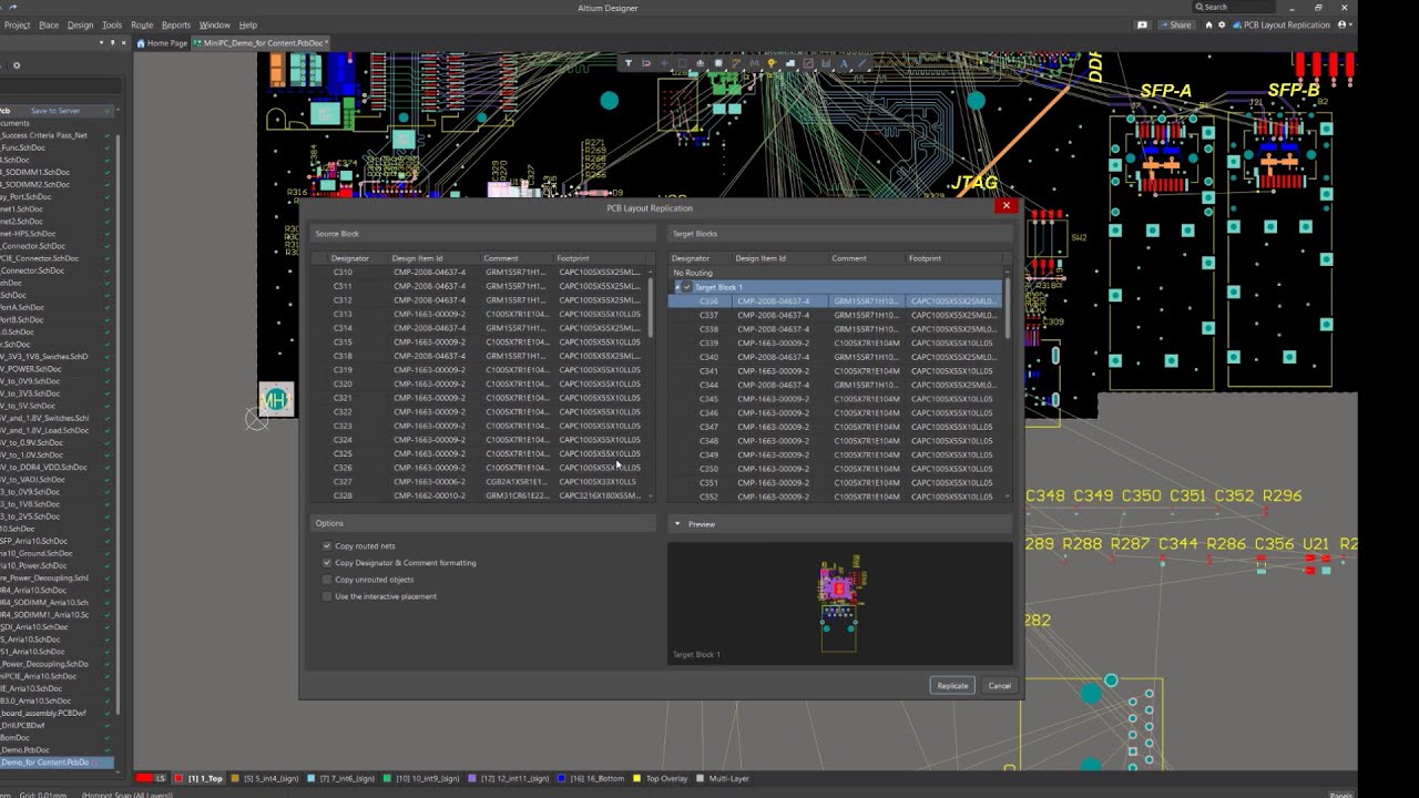
Manually Map Components with PCB Layout Replication
You now have the ability to manually map components in target blocks where multiple components have been detected by the PCB Layout Replication Tool as having similar connections. This allows you to manually choose between available components that are able to replace each other, without violating circuit connectivity.
RECOMMENDED CONTENT
- Witness the benefits of using the PCB Layout Replication tool in this short video.
- To see the PCB Layout Replication in action, check out our demonstration video.
- Visit the PCB Layout Replication documentation page to learn more.
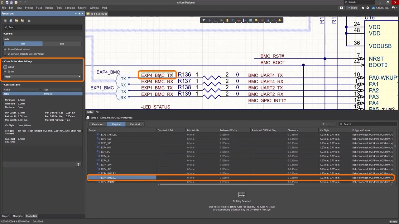
Constraint Manager Enhancements
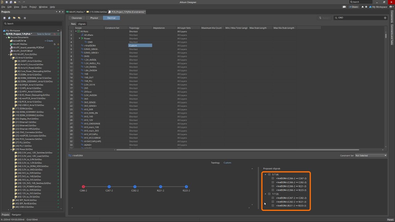
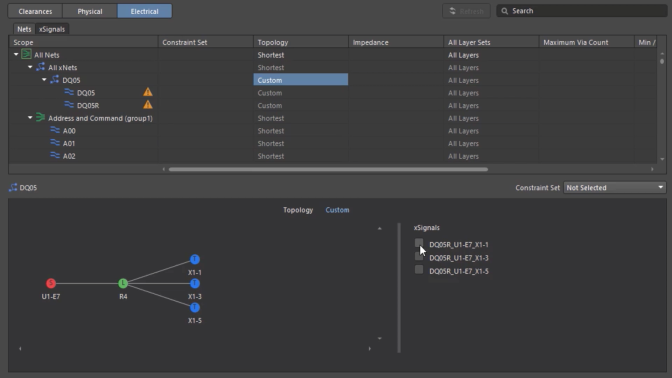
Experience a Heightened Level of Control with the Constraint Manager
Altium Designer's Constraint Manager, with significant enhancements in design control, is now more flexible and intuitive. Efficiency in design organization is improved with the capability of adding nets to an existing class. Custom topologies are defined more insightfully with structured xSignals, and we’ve also added line numbers on tabs/grids to enhance clarity and navigation. Lastly, you can now choose between the Constraint Manager and the older Design Rules system when creating a new project to adapt to your preferred workflow.
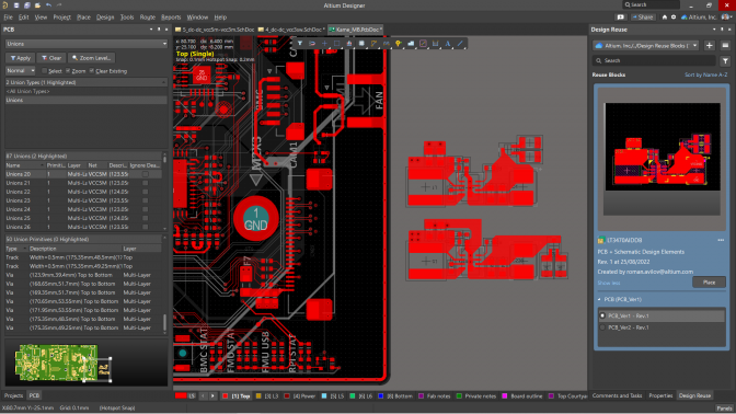
PCB CoDesign Improvements
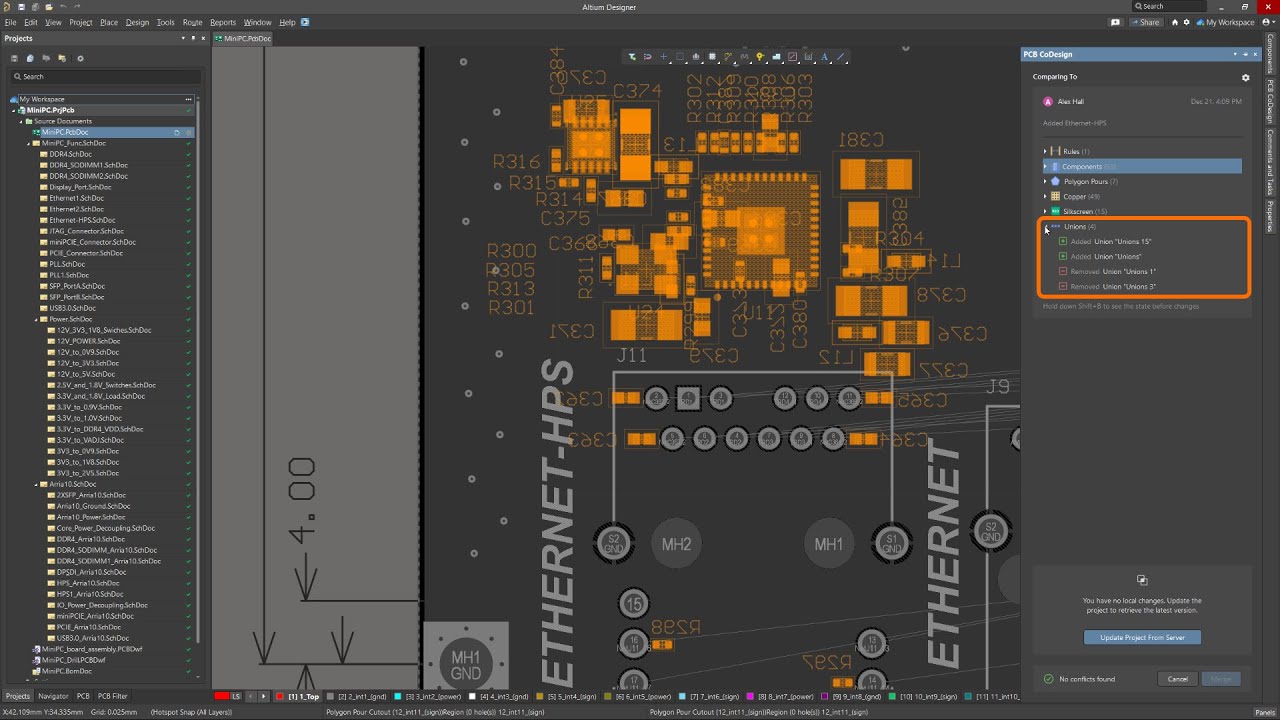
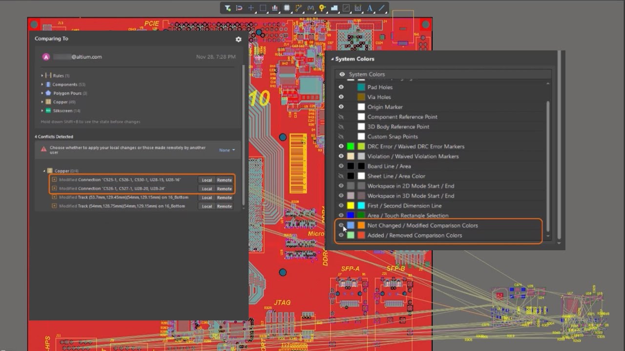
Highlight Specific Modified Categories with PCB CoDesign
Altium Designer's latest PCB CoDesign enhancements offer a more efficient and streamlined collaboration process. You can now precisely compare and apply changes to unions for targeted modifications. Also, the ‘Show on PCB’ option simplifies highlighting changes in specific categories for better visualization. These improvements aim to boost efficiency and provide a more organized and seamless collaborative design experience.
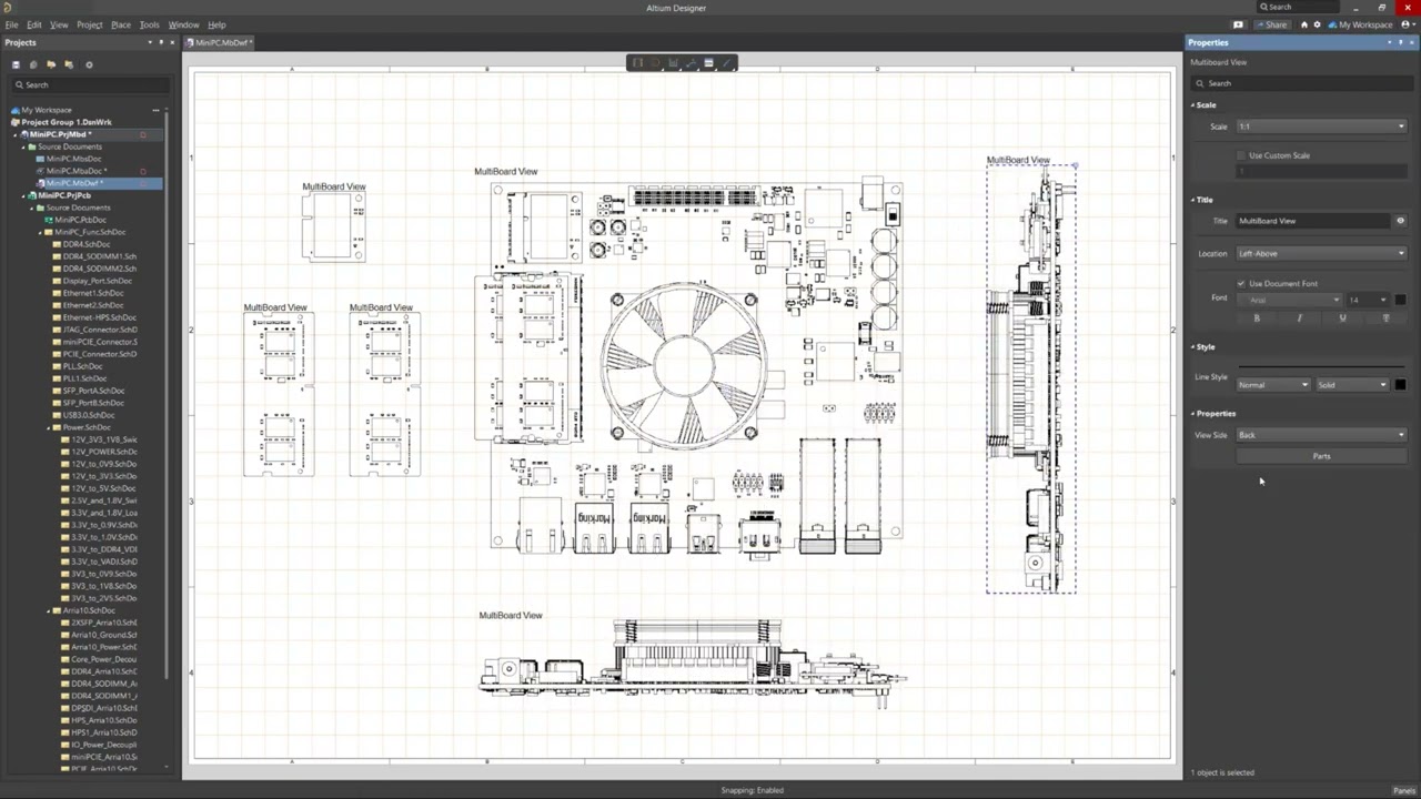
Multi-Board Improvements
Create a Clear Visual Representation of your Multi-Board Project
Altium Designer's Multi-board Draftsman tool integrates manufacturing drawings into Multi-board design projects. The multi-board view displays combined graphics of PCB outlines and 3D models with various viewing options. Enjoy standard Draftsman features like annotation, dimensioning, and BOM, and say goodbye to managing different documentation sets or relying solely on MCAD software. Draftsman for Multi-board offers a clear visual representation of board connections in larger systems, ensuring design integrity and consistency.
Simulation Improvements
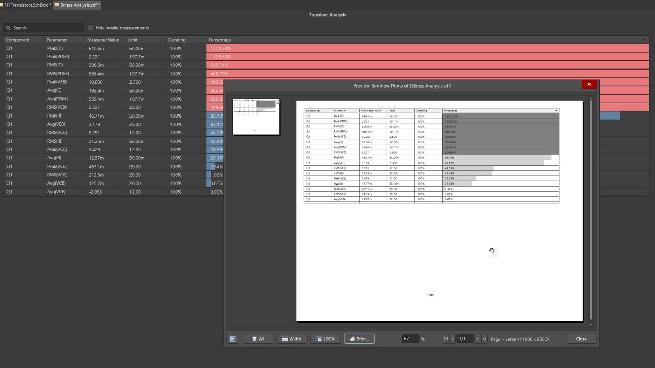
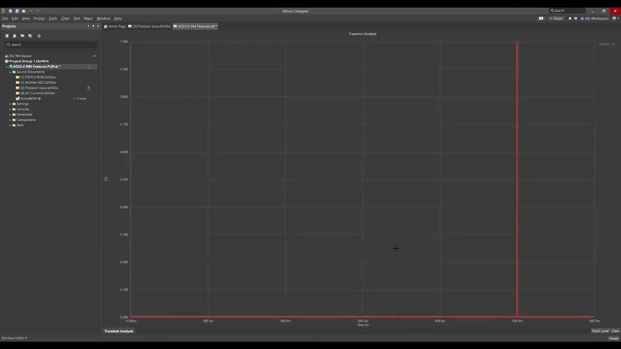
Make Informed Component Decisions with Stress Analysis
Altium Designer introduces the Simulation Stress Analysis tool, which enhances the design process by incorporating stress analysis within transient analysis. This tool calculates and checks component operating conditions against defined limits, simplifies stress model creation, and allows for reliability derating. With a comprehensive stress chart in the simulation viewer, it provides precision and control for informed decisions on component reliability and performance.
Simplify Complex Design Rules with the Constraint Manager
Altium Designer's Constraint Manager, available for pro and enterprise subscriptions, simplifies meeting complex standards and PCB design requirements. This tool allows easy browsing, creation, modification, and reuse of verified constraint sets through a tabular, object-based user interface. Enhancing clarity and comprehension, it seamlessly integrates rules between schematics and PCB layout, streamlining the design process with a consistent format for rule addition in both areas.
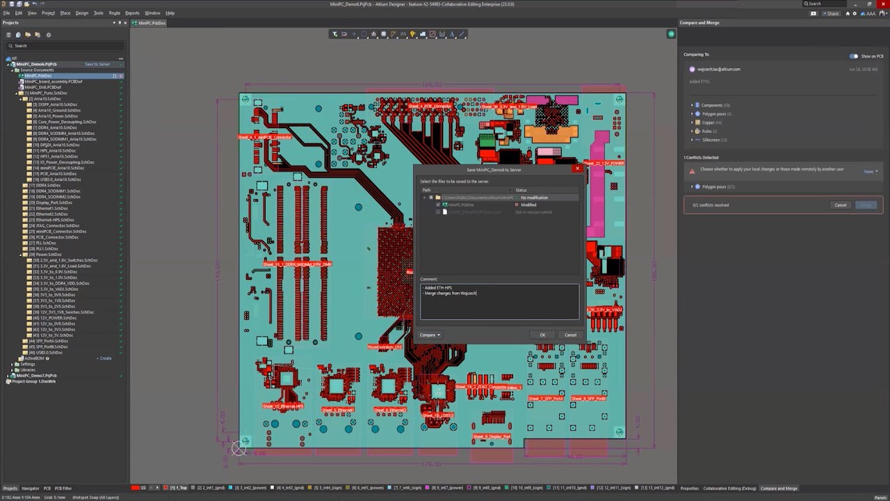
Work Together and Design Faster with PCB CoDesign
Altium Designer's PCB CoDesign simplifies collaboration, ensuring design integrity for engineering teams. With pro and enterprise subscriptions, this tool streamlines cooperation within your workspace, eliminating manual change tracking. Visualize alterations, compare layouts, and merge updates effortlessly in a unified environment. Say goodbye to cumbersome revision histories and embrace a more efficient PCB design approach with PCB CoDesign.
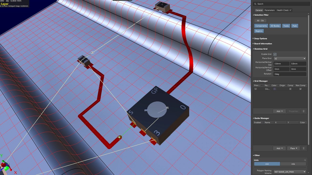
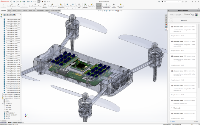
Elevate Your Projects with the 3D Mechatronic Integrated Device Tool
Altium Designer introduces the groundbreaking 3D Mechatronic Integrated Device design tool, simplifying the integration of non-planar electronic designs. It seamlessly aligns with existing components, synchronizes with schematic documents, and eliminates the need for time-consuming M-CAD hacks. This tool meets electrical specifications while enabling aesthetically pleasing designs. With pro or enterprise subscriptions, it facilitates easy adoption in your product development workflow.
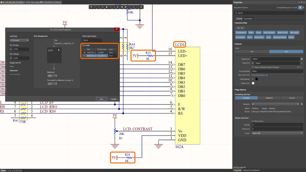
Assign Currents to Multiple Nets with the Power Analyzer by Keysight
Altium Designer's enhanced Power Analyzer by Keysight Tool addresses power network analysis challenges efficiently. With new support for assigning currents to multiple nets on the same component across different series elements. This enhancement ensures a seamless and efficient power analysis experience, allowing you to maximize benefits from your design in Altium Designer.
Altium Designer 23
Tackle Any Design Complexity With the Constraint Manager
Speed Up Your Workflow With the Power of PCB Layout Replication
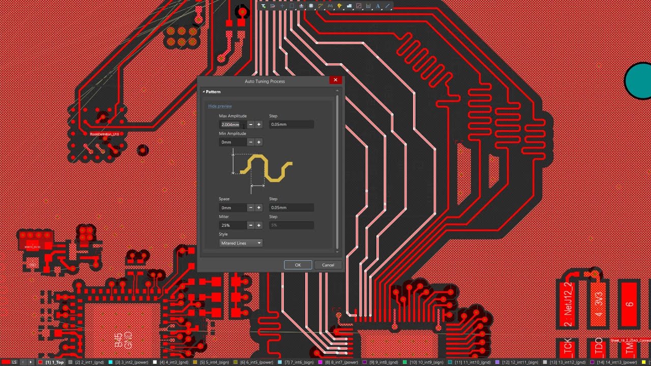
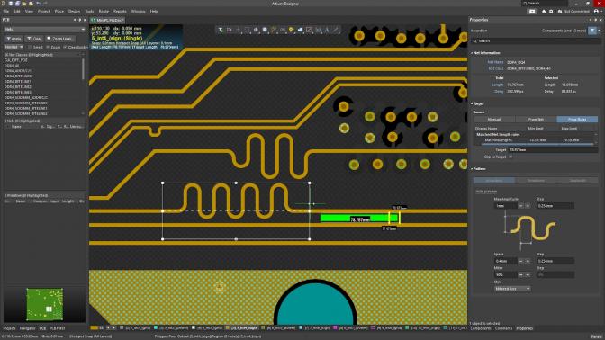
Minimize Manual Effort With Automatic Length Tuning
PCB Improvements
Easily Edit Paste and Solder Mask Shapes
PCB Improvements
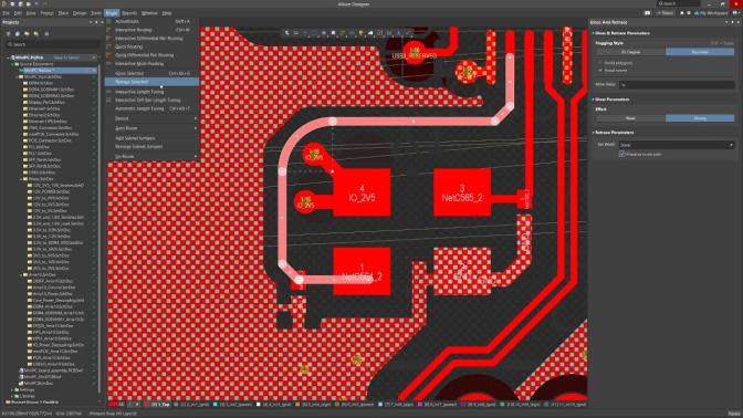
Retrace Single-Ended Traces at any Angle
We've added a new "Retrace Parameters" feature to the Gloss and Retrace panel, offering enhanced flexibility for retracing single-ended traces at any angle using the Rounded hugging style. You can also set rule-based width modes or input custom values to ensure compliance with design rules. Furthermore, you have the option to "Preserve Route Path," allowing you to maintain precise trace geometry during retracing, providing greater control and design accuracy.
Component Management Improvements
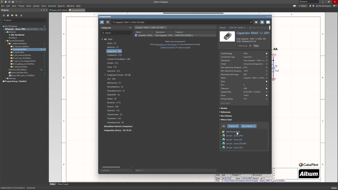
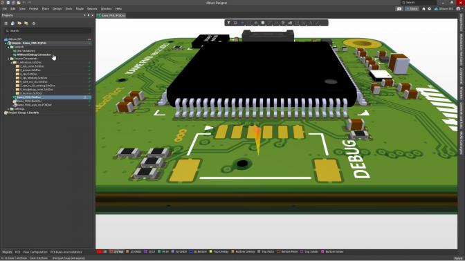
Track Components in Reuse Blocks with the “Where Used” Panel
Altium Designer's "Where Used" component panel streamlines component management in your PCB designs. It offers a comprehensive list of where each component is used, making conflict resolution and maintaining design accuracy a breeze. The latest enhancement features a redesigned panel and integration of Reuse Blocks from the connected Workspace's library, with tabs displayed only when relevant to reduce clutter.
Collaborative Improvements
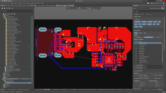
Efficient Concurrent Design with PCB CoDesign
For Pro and Enterprise subscriptions, PCB CoDesign in Altium Designer revolutionizes collaborative design by enabling multiple team members to work simultaneously on a project, ensuring streamlined development, efficient testing, and faster iteration to meet project deadlines. This feature includes Git-like version control, allowing collaborators to access the same project concurrently, commit changes to a master branch, and use Commenting and Tasks features to allocate work on the board. Notifications alert team members of commits, and the Compare and Merge panel displays differences in design, offering color-coded feedback. When conflicts arise, such as overlapping changes by multiple designers, you can confidently decide to keep local changes or accept remote changes from the latest commit, ensuring a smooth collaborative design process.
Importer Enhancements
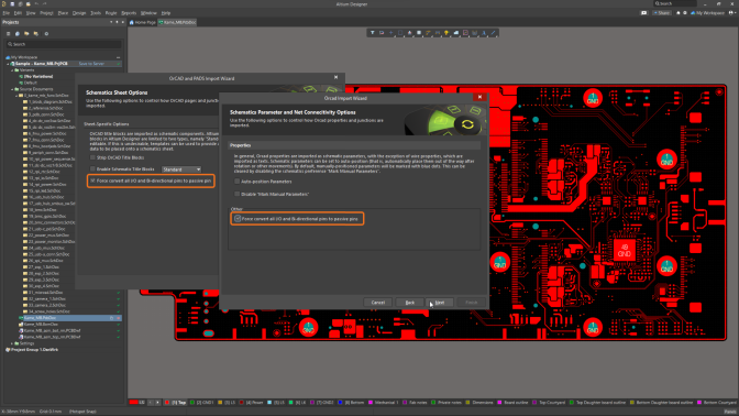
Seamlessly Import OrCAD and Allegro Design Files
There are key improvements and fixes in relation to the import of OrCAD and Allegro design files into Altium Designer. This includes support for customized port connectors, accurate title block parameter handling, component fill coloring preservation, and precise design file imports, ensuring your design process is seamless.
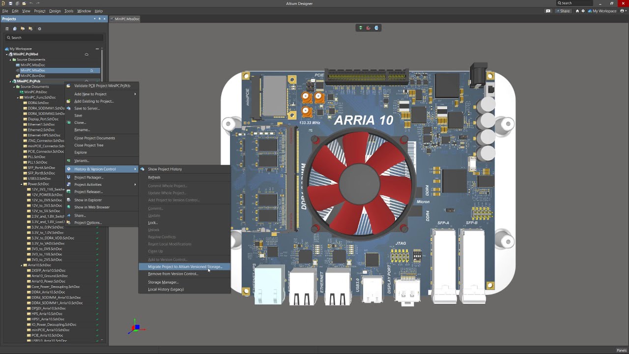
SVN-to-Git Migration
Migrate Projects from SVN to Git in Your Enterprise Server Workspace
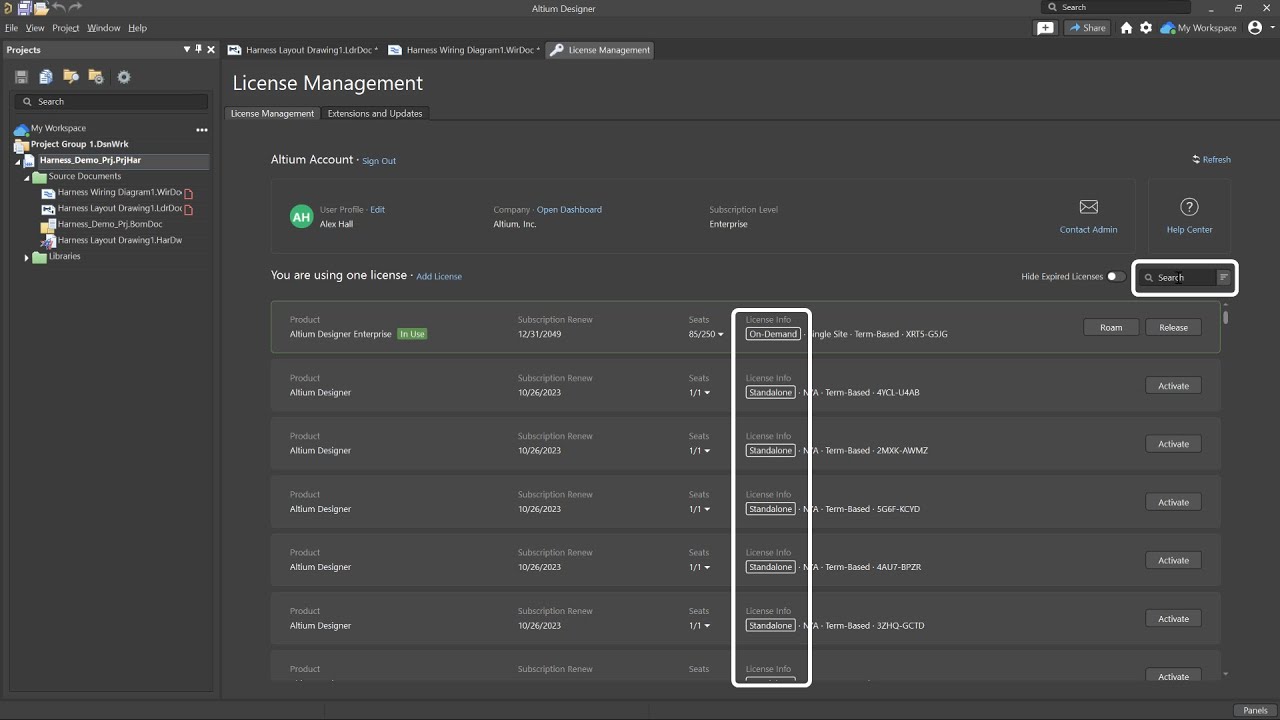
License Management Improvements
Optimize License Management with Enhanced Navigation and Labels
Harness Design Improvements
Unlock More Efficient Harness Design Features and Easily Validate Projects
For Harness Design, the zoom level now sets the size of the model view's green box automatically. No need for manual adjustments. We've also added quick keyboard shortcuts for adding wires and placing bundles to streamline your workflow. Plus, you can easily validate your active harness project with the new validate button.
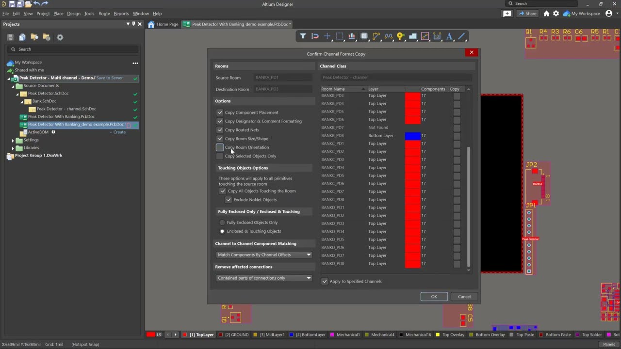
PCB Design Improvements
Simply Copy Room Format with Rotation
PCB Design Improvements
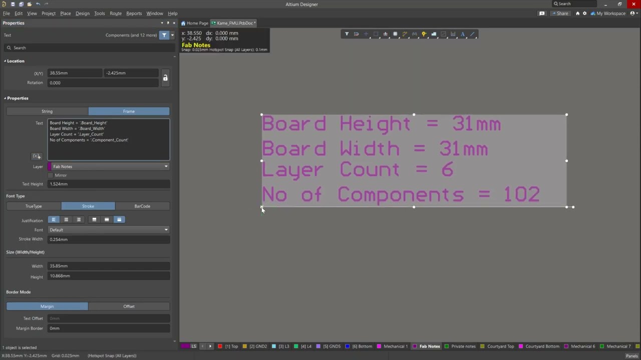
Add New Special Strings for Fabrication and Assembly Notes
You can now include a wider range of manufacturing and assembly parameters, such as layer counts, board dimensions, and object quantities directly into your fabrication and assembly notes. These additions are conveniently auto-calculated directly from the PCB, ensuring that your notes align with any design updates.
PCB Design Improvements
Freely Customize Paste Mask and Solder Mask
PCB Design Improvements
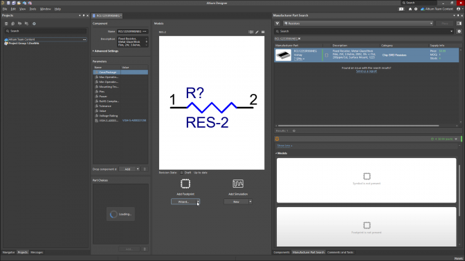
Conveniently Manage Part Choices for Each Component in Your Design
Circuit Simulation Improvements
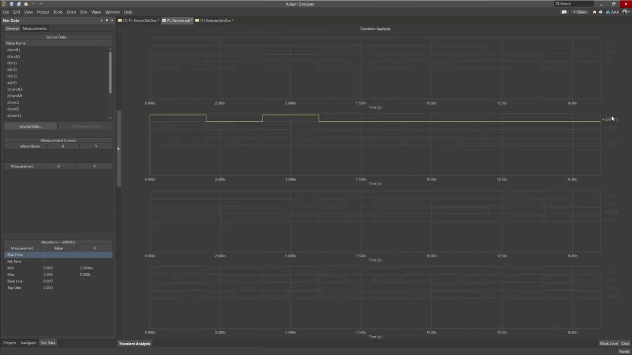
Precisely Measure your Results with the New Simulation Data Viewer
The new Mixed-Simulation Data Viewer introduces higher waveform accuracy and measurement precision. This extended precision significantly reduces the likelihood of round-off errors, ensuring more accurate results when viewing simulation waveforms to improve the overall reliability of the simulation process.
Harness Design Improvements
Easily Keep Track of your Harness Wiring Diagrams
Altium has expanded support for additional multi-board features, which allows you to navigate to your wiring diagrams seamlessly from your multi-board schematic. You are now able to cross-probe directly from the corresponding harness object on the multi-board schematic to the Wiring Diagram of that harness design, minimizing the risk of mismatch and giving you more control over your multi-board design.
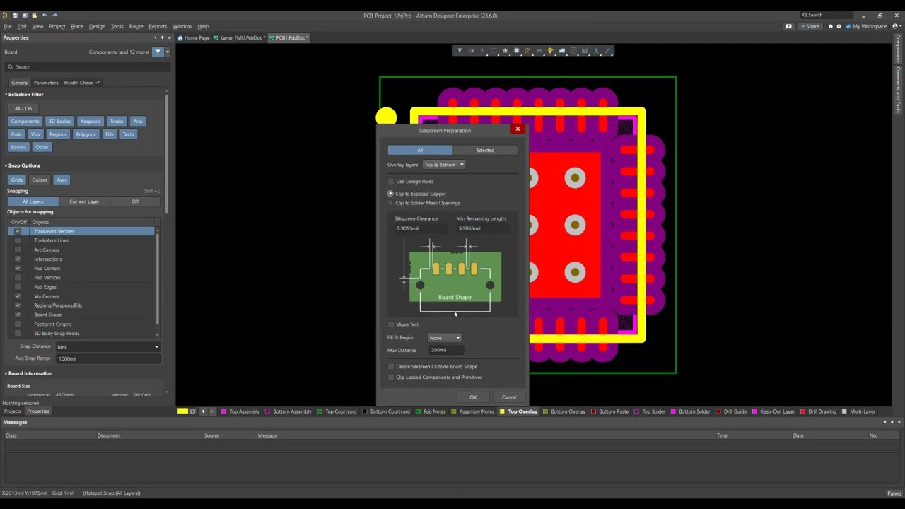
PCB Design Improvements
Precisely Position Silkscreen for Footprint Creation and PCB Manufacturing Preparation
The latest release simplifies the management of the silkscreen preparation process, offering the ability to effortlessly move or clip silkscreen objects at specific distances from exposed copper or solder mask openings. This eliminates the need for manual silkscreen work while creating footprints and PCB manufacturing preparation.
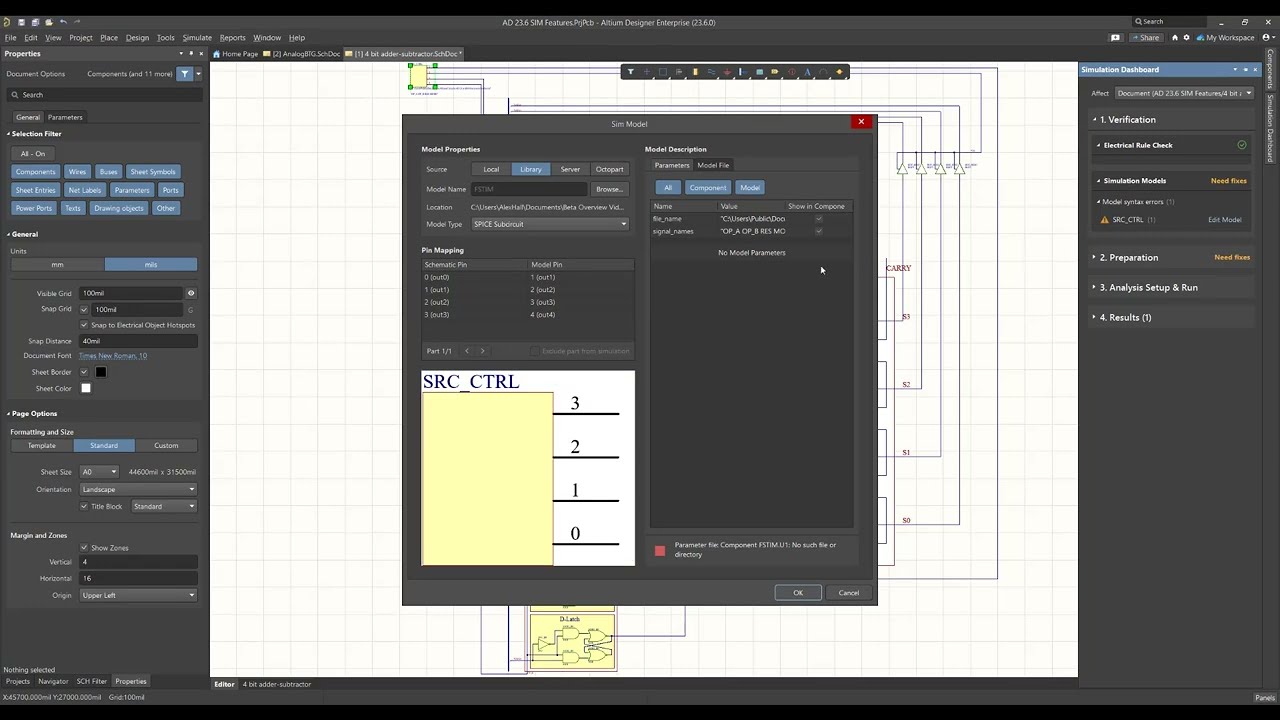
Circuit Simulation Improvements
Utilize the FSTIM Stimulus Model During Simulation
Altium's latest release adds simulation capabilities by providing expanded support for additional components. You are now able to add your digital file stimulus device (FSTIM) model primitives from PSpice for simulation in Altium to achieve high accuracy and efficiency in generating transient signals. This addition aligns with Altium's ongoing commitment to have a best-in-class SPICE simulator fully integrated within the Altium Designer environment.
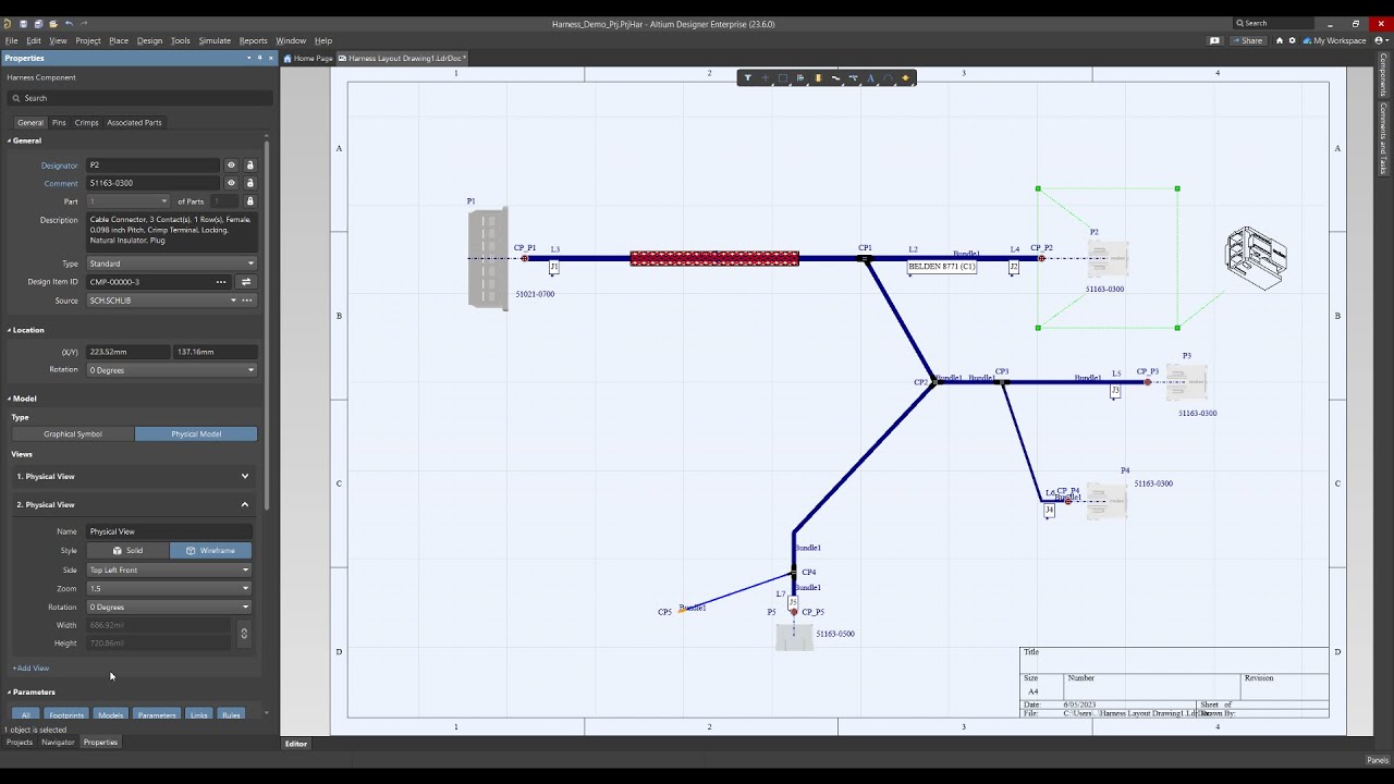
Harness Design Improvements
Create Your Harness Cable Assembly Drawing Even More Precisely
This release introduces new tools for precise harness cable design, helping to reduce errors during assembly. You can now define the size of the harness covering relative to the enclosed bundle and choose between solid-style and patterned fills. Additionally, isometric views in the Layout Drawing give assemblers an additional viewpoint to enhance the presentation of harness components, enabling comprehensive communication of design intent and minimizing assembly errors.
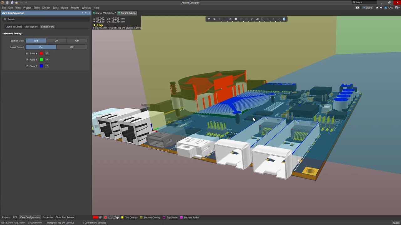
Discover the hidden parts of your board with the pcb section view
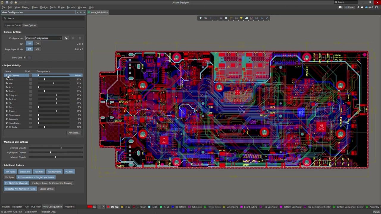
The PCB section view provides precise insight into the layout and structure of your designs, like never before. when working with dense and complex PCBs the section view reveals the details within a PCB that are typically not visible. With full control over plane placement and color you can easily see all components, even smaller SMD components hiding under larger components or mechanical parts.
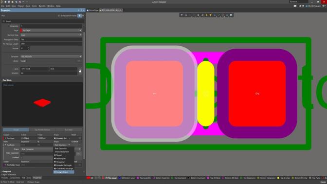
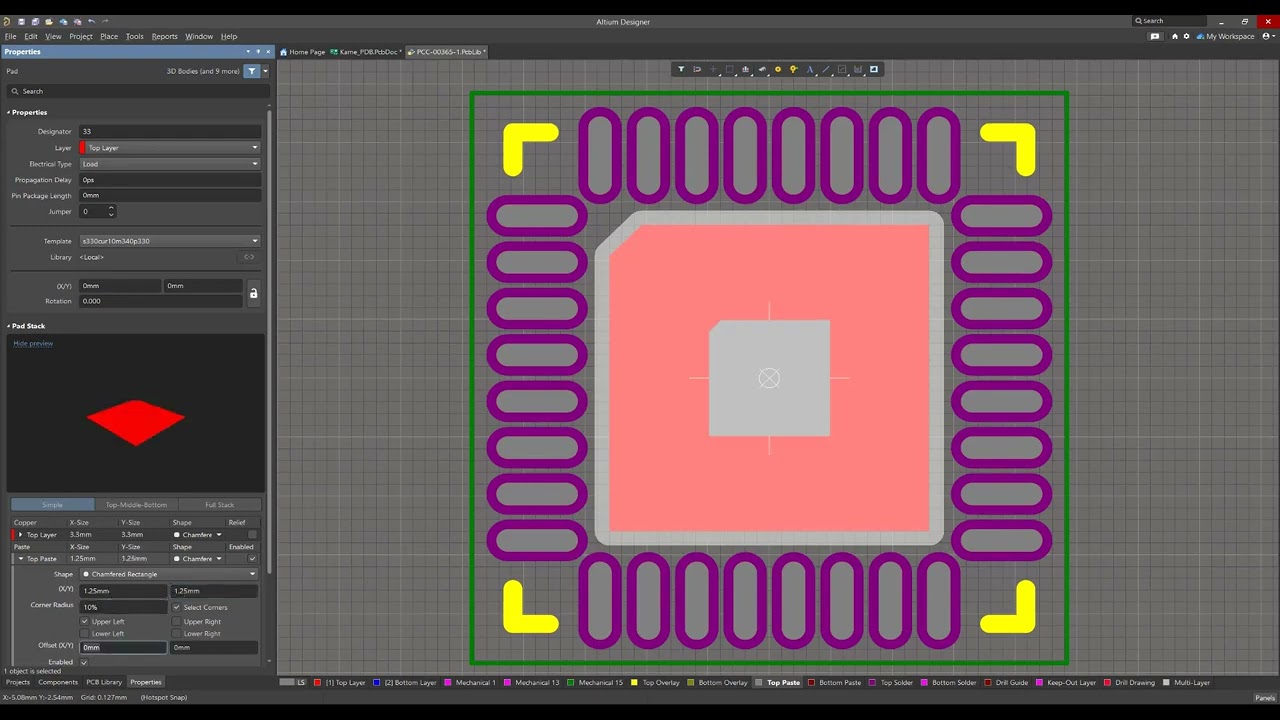
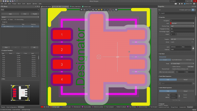
Custom Thermal Reliefs for Pads
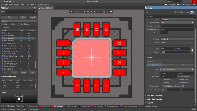
As a continuation of our custom pad shape capabilities, it is now possible to add, remove, and edit, thermal relief spikes to anywhere on a pad, regardless of shape. This helps with soldering and avoids possible manufacturing problems like tombstoning.
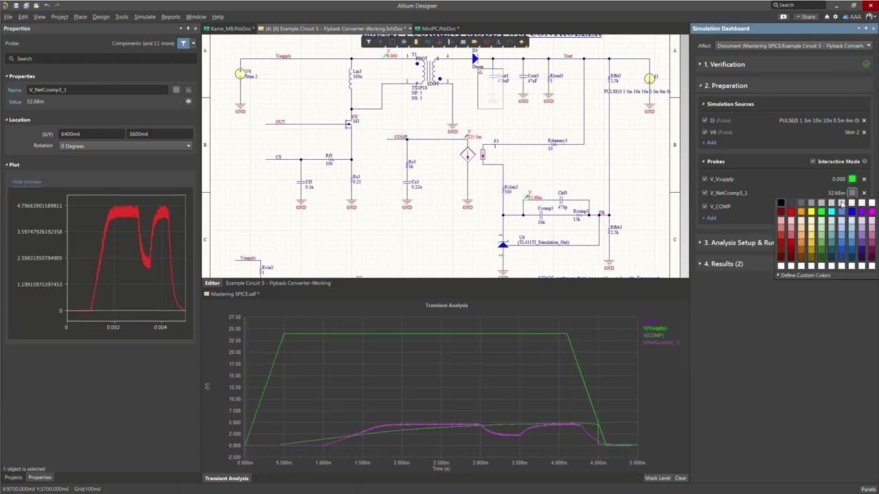
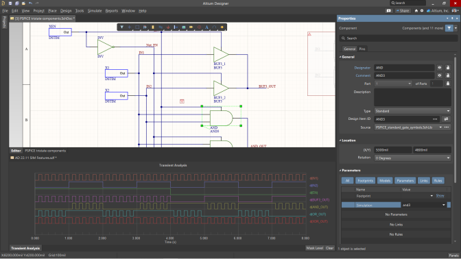
Test Your Circuits With Real-Time Simulation Probes
The interactive probes feature is like using an oscilloscope right within Altium Designer. When this feature is enabled, any changes to probe placement, color, or other settings, are immediately reflected in the simulation results document.
Circuit Simulation support for Output Values in AC Analysis for Controlled Sources and Variable Passives
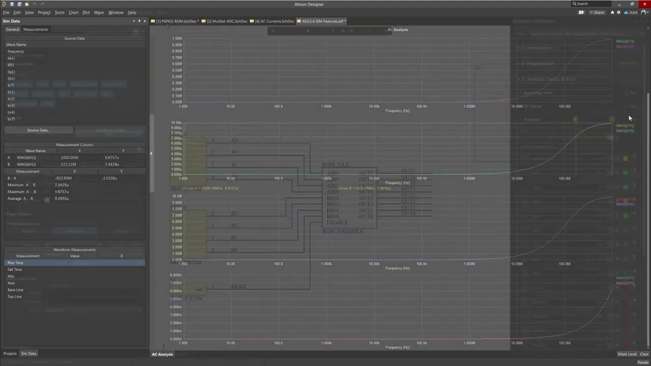
We’ve now added support for voltage and current controlled sources, functional sources and variable passive components for voltage, power and current output variables in the AC analysis. Great for audio projects, communication designs, and other design types. Plus we’ve added support for multi-bit ADC and ROM PSPICE digital model primitives as well as their timing models.
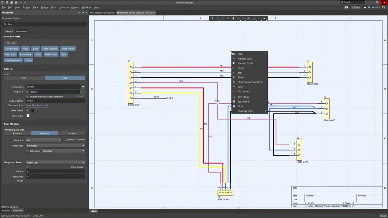
Live Traces & Fixed Aspect Ratios for Harness Wiring Diagram Objects
Live traces actively follow your cursor, showing you the way to your final wire destination. Allowing you to move more efficiently in the wiring diagram. Wiring diagram objects are now synced with the documents snap grid, bringing a new level of uniformity to the diagram.
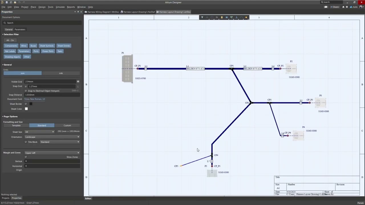
New in Harness Design: 3D wireframe View And Ability to Add Models to Connection Points
In the Layout Drawing, it is now possible to show the Physical (3D) model for a connector as a wireframe view and also, for a connection point, display the Physical (3D) model of one of its associated parts.
Support For Workspace Defined Parameters & Bulk Edits For Components
For this release we have added support for workspace defined project parameters, bulk creation and edits of components, and enhanced side-by-side component revision comparison.
Added Support for Variable Passives & Global Nodes
This release of Altium Designer we’ve added support for more programmable logic array PSPICE digital primitives as well as support for digital models that use global nodes ($D_HI, $D_LO, $D_X), and variable passives.
Harness Design Improvements
The wiring diagram and layout drawing for harness projects has been given several new features to boost usability. We’ve added additional crimping capabilities, scaling options for documentation, visual connection lines for components and more.
PCB IMPROVEMENTS
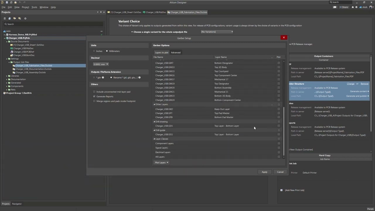
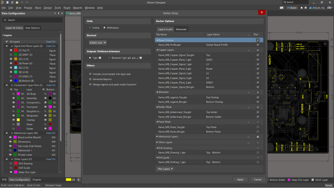
Gerber Setup Layer Class Support
The Gerber Setup dialog now includes a Layer Classes section in its Layers to plot list. Using the checkbox for layer classes, you can quickly enable plotting for all the layers that belong to a specific layer class.
Circuit Simulation Improvements
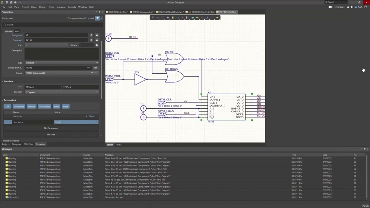
Added Support for PSpice Digital models
This release of Altium Designer supports even more PSPICE digital model primitives. We’ve added support for the PINDLY, and CONSTRAINT Pspice digital behavioral model primitives as well as support for the DIGRRGEFAULT option.
Harness Design Improvements
Harness Design Improvements
In this release of Altium Designer we’ve added several new features to boost the usability of the harness wiring diagram and layout drawing. Including additional features for crimping, splices, and efficiency
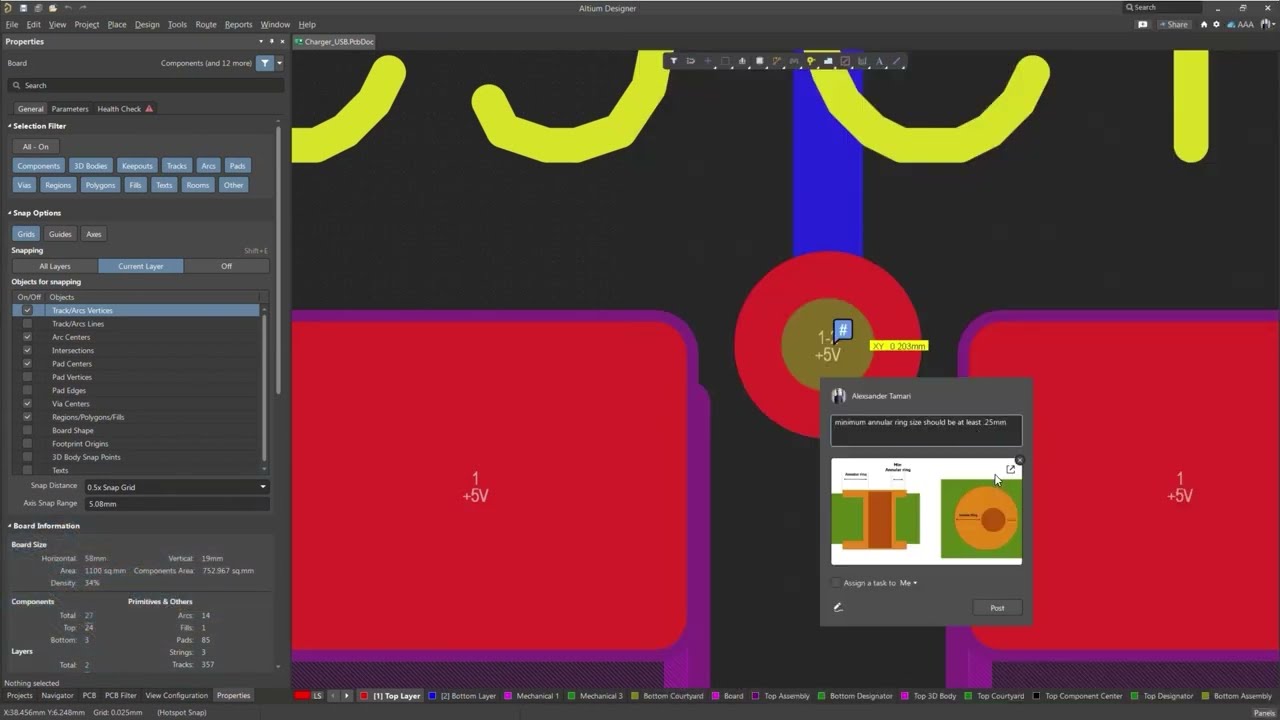
DATA MANAGEMENT IMPROVEMENTS
Update to Collaboration and Reporting
To better convey a message to other project stakeholders, you now have the capability to copy and paste pictures into your comments. Also, exporting a project history report can now be easily done through the Reports menu.
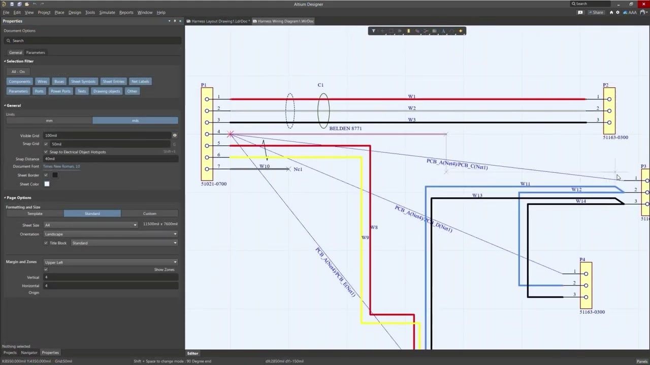
HARNESS DESIGN IMPROVEMENTS
Additional Harness Design Capabilities
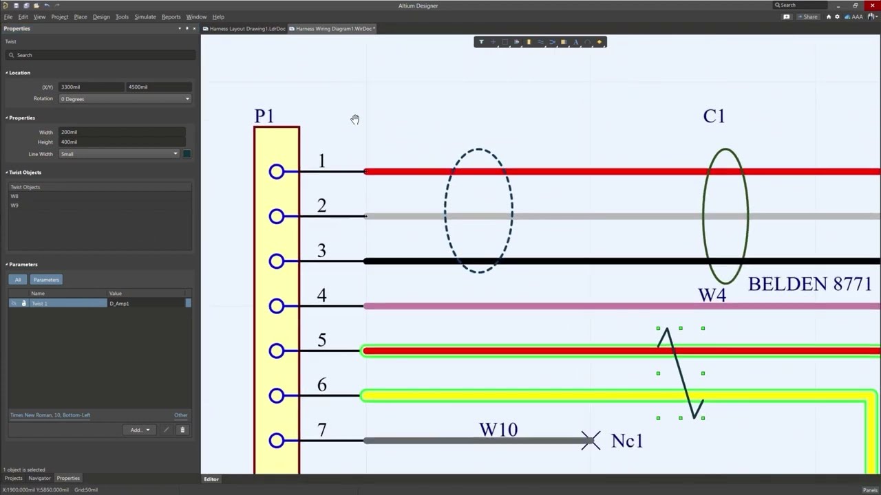
This release has added several improvements for both the harness wiring diagram and the Harness layout drawing. Some new capabilities include: parameters for twist and shield objects, crimping, additional 3D views, multiple connections from a single point and more…
PCB IMPROVEMENTS
New PCB Capabilities for Gerber and View Configuration
New PCB features allow you to load a stored view configuration file from the View Configuration Panel. Also, it is now possible to change the name for the Gerber Board Profile layer when using the new, unified Gerber/Gerber X2 dialog.
SIMULATION IMPROVEMENTS
New Extension For Power Integrity Analysis
Quickly assess the integrity of your power distribution network without the need for any specialized training with Power Analyzer by Keysight.
PRODUCT DESIGN IMPROVEMENTS
Multi-board support In MCAD CoDesigner
You are now able to transfer and sync your muli-board designs with your mechanical team using the MCAD CoDesigner.
PRODUCT DESIGN IMPROVEMENTS
New Harness Design Capabilities
Harness Design functionality allows you to create a full wiring harness design, from the individual pin-to-pin connections right through to manufacturing documentation.
Altium Designer 22
PCB Improvements
Custom Pad Shapes with Rounded/Chamfered Corners
Shape your pads the way you need in a matter of clicks. Extending the versatility of pad shapes, you can now customize the rounding of selected corners of pads that use either the Rounded Rectangle shape or the new Chamfered Rectangle shape.
PCB Improvements
Enhanced Gerber Setup Interface
Efficiency, simplicity and convenience are all delivered with the new UI for Gerber setup. Everything you need to prepare for Gerber generation is now at your fingertips in an intuitive setting.
SPICE SIMULATION IMPROVEMENTS
Additional Digital Models & Variant Support
Expanding the functionality available to you in the simulation arena, this release adds further support for PSPICE digital gates, timing and I/O models. Support for variants is also now available.
Data Management Improvements
Improved Manufacturer Part Search UI
The Manufacturer Part Search panel has long been a source of components for many users. Improvements have been made in this release that make it easier to use components in their libraries. This allows you to spend more time on development than on the process!
PCB Improvements
Additional Net Information for Tuning Objects
Detailed net information about tuning objects has been added in this release. Information about the maximum current and active resistance of accordion, sawtooth, and trombone objects is now available. More detail means it is less likely mistake will be made!
Schematic Capture Improvements
Quickly View Multi-function Pin Names
A large number of microcircuits have multi-functional pins. Working with them in Altium Designer has become even easier. This release introduces the ability to display the alternative pin names with just one click.
Schematic Capture Improvements
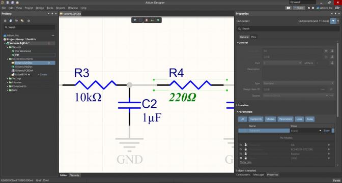
Improved Variant Management
Variant management is taken to the next level with this release. Time spent creating and editing variants is greatly reduced. Now you can design with large numbers of variants with streamlined ease and efficiency.
Data management improvements
BOM Commenting
Support for commenting has arrived in the BOM arena with this release. All stakeholders can actively discuss the BOM with ease and convenience, as enjoyed already with schematic and PCB documents.
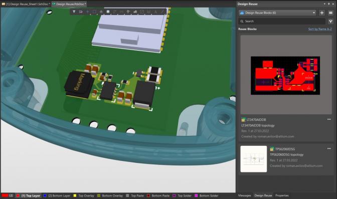
Data Management Improvements
Alternative PCB Layouts in a Reuse Block
Reuse Blocks are enhanced further in this release. You can now define multiple, alternate PCB layouts for use with a single block. When placing a block, quickly switch layouts to suit your physical and performance needs.
Data Management Improvements
Design Reuse Functionality
Take the enhanced functionality of Reuse Blocks for a spin in this release, with the ability to place a block (or schematic snippet) as a sheet symbol. Your proven circuitry is placed on an auto-generated child sheet.
Schematic Capture Improvements
Mark Multiple Components as Fitted/Not Fitted
With this release it becomes even easier to work with multi-variant design projects. Now you can select multiple components for the active variant and mark them as Fitted/Not Fitted in a single action.
PCB Improvements
Custom Pad Shapes
Modern components often contain pads that are complex in shape. This release of Altium Designer gives you the ability to create custom pad shapes quickly and easily, with management similar to that of standard pads.
PCB Improvments
Ability to Change Tuning Object Layer Properties
Design of high-speed PCBs becomes easier with this latest release. Now, when you need to quickly move tuning elements to a different layer, you can do so from the Properties panel with a single click.
SPICE Simulation Improvements
Auto-assign Simulation Models for Components without Models
This latest version of Altium Designer makes schematic simulation even easier. System intelligence automatically recognizes SPICE models and assigns them to components from available sources.
Output Improvements
Control of Paste Mask Output for Variants
Output data needs to be as accurate as possible. For multi-variant designs you can now ensure that the paste mask is only displayed where it is really needed.
PCB Improvements
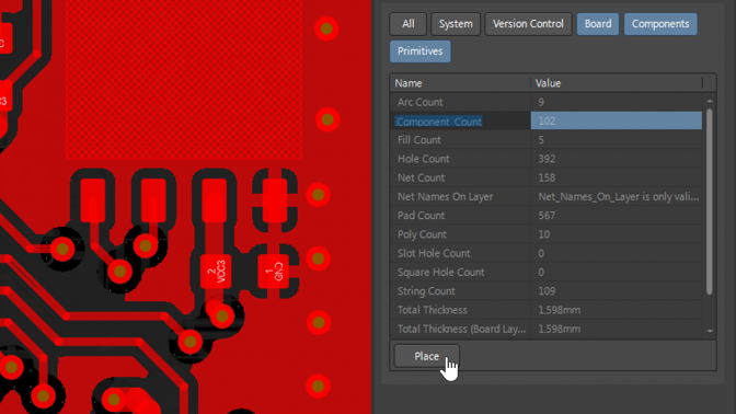
Quick Browsing of Parameters for a Board
Parametric information for your board is now conveniently available from the Properties panel. A single, convenient location with which to browse system, calculated and user-defined parameters, and place as needed in the form of special strings.
Schematic Capture Improvements
Active Links in Text
You can now specify active links to components and nets within a text frame object on a schematic. This handy navigation aid makes it much easier not only to read the document, but also to work with it.
Schematic Capture Improvements
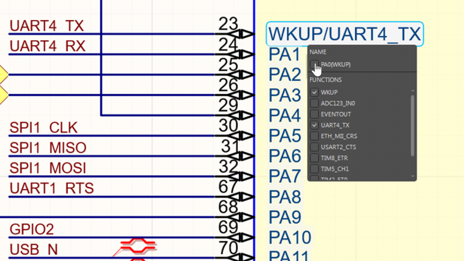
Multifunctional pins
You will often see that modern ICs consist of multi-functional pins. In this latest version of Altium Designer it has become far easier and much more convenient to work with such components.
Schematic Capture Improvements
Custom Diff Pair Suffixes
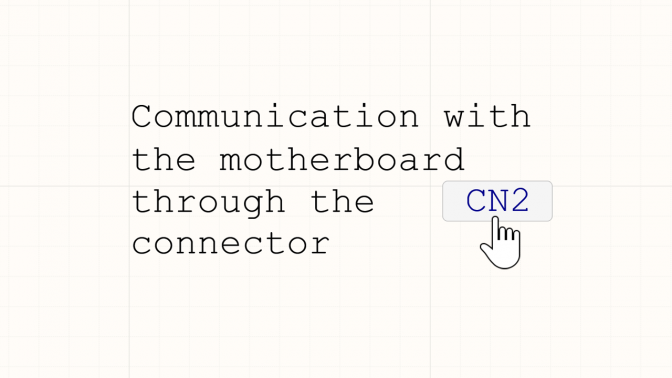
Even more possibilities for creating differential pairs. Now you can use any postfixes to designate positive and negative net of a differential pair.
PCB Improvements
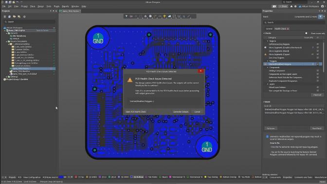
PCB Health Check Monitor
The condition of the PCB is under your control. A new intelligent feature that gives you confidence that your PCB is okay and complies with design rules.
Schematic Capture Improvements
Display of Alternate Component Parameters
Many schematic solutions are created as multivariant. With the new release, the schematic of multivariant project have become even more detailed and informative.
MultiBoard Improvements
Components from Altium 365
Working with multiboards has become easier and more convenient. Now you have more component sources at your disposal.
Data Мanagement Improvements
New Design Reuse Functionality
A reuse bloks help reduce development time and avoid errors. The new Design Reuse Panel and new functionality expands the possibilities for reuse blocks and snippets.
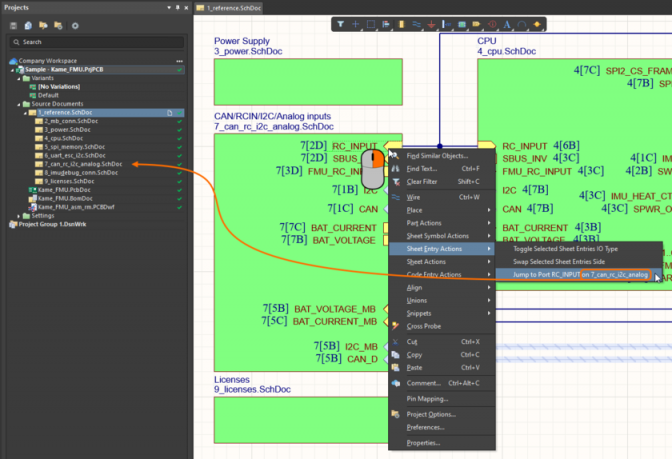
Further Enhancements to Sheet Cross-referencing
Schematic Capture Improvement
Adding cross-references to the project allows you to easily follow the connective flow of nets between the schematic sheets in a project.
High-Speed Design Improvements
Relative Length Tuning
Designing high-speed PCB just got easier. The Length Tuning tools is now even more functionality. Complex tasks can now be solved even faster.
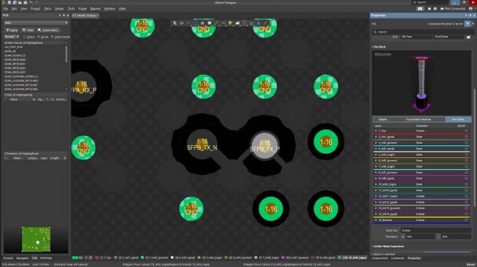
PCB Design Improvements
Enhanced UI for Via Stack Editing
The via editing mode is now even more convenient. Information about the via, editing its parameters and connections to polygons are now all in a new and simple, but familiar form.
Data Мanagement Improvements
Generic Components
The way from idea to real devices has become shorter. The new feature will reduce the time it takes to design a schematic.