A variety of objects are available for use in designing a PCB. Most objects placed in a PCB document will define copper areas or voids. This applies to both electrical objects, such as tracks and pads, and non-electrical objects, such as text and dimensioning. It is, therefore, important to keep in mind the width of the lines used to define each object and the layer on which the object is placed.
There are two types of objects in the PCB editor – primitive objects and group objects:
-
Primitive objects are the fundamental elements of design and include tracks, pads, vias, fills, arcs, and text objects. They are called 'primitive' due to their raw or most basic nature.
-
Anything that is made up of primitives and identified as a design object is a group object. Examples of group objects include components, dimensions, and polygon pours. A group object can be manipulated as a single object within the design space. For example, it can be placed, selected, copied, changed, moved, and deleted.
Object Placement and Editing Commonality
In Altium Designer, the process of placing an object is roughly the same regardless of the object being placed. At its simplest level, the process is as follows:
-
Select the object to be placed from one of the toolbars or the Place menu.
-
Use the mouse to define the location of the placed object in the PCB editor design space and its size (where applicable).
-
Right-click (or press Esc) to terminate the command and exit placement mode.
Objects are placed on the current layer. Ensure the correct layer has been made the current layer before effecting placement. The layer on which an object resides can be changed after placement.
Editing Prior to Placement
The default properties for an object can be changed at any time on the PCB Editor – Defaults page of the Preferences dialog. These properties will be applied when placing subsequent objects.

Use the Primitives column to access properties for objects and edit default values as required.
Default values for the objects are saved, by default, in the file ADVPCB.dft. Optionally, values can be saved in a .dft file with a different name. Controls are available to save and load .dft files, enabling you to create favorite default object value 'sets'. All settings saved in and loaded from .dft files are user-defined defaults. Should it be necessary, original default values can be brought back at any time using the Set To Defaults or Reset All options. The original default values are hard-coded.
Editing During Placement
A number of attributes are available for editing at the time an object is first placed. To access these attributes, press the Tab key while in placement mode to open the associated Properties panel. Pressing the Tab key pauses placement in order for you to make any required edits for the object.

Example properties dialog for a Pad object.
After edits have been made, click the design space pause button overlay (  ) to resume placement.
Attributes that are set in this manner will become the default settings for further object placement unless the
Permanent option on the
PCB Editor – Defaults page of the
Preferences dialog is enabled. When this option is enabled, changes made will affect only the object being placed and subsequent objects placed during the same placement session.
Editing After Placement
Once an object has been placed, there are a number of ways in which it can be edited. These are described below.
The Associated Properties Panel or Dialog
This method of editing uses the associated Properties panel mode and dialog to modify the properties of a placed object.
After placement, the associated dialog can be accessed by:
-
Double-clicking on the placed object.
-
Placing the cursor over the object, right-clicking then choosing Properties from the context menu.
After placement, the associated mode of the Properties panel can be accessed in one of the following ways:
-
If the Properties panel is already active, select the object.
-
After selecting the object, select the Properties panel from the Panels button at the bottom right of the design space or select View » Panels » Properties from the main menus.
If the
Double Click Runs Interactive Properties option is disabled (default) on the
PCB Editor – General page of the
Preferences dialog, when the primitive is double-clicked or you right-click on a selected primitive then choose
Properties, the dialog will open. When the
Double Click Runs Interactive Properties option is enabled, the
Properties panel will open.
While the options are the same in the dialog and the panel, the order and placement of the options may differ slightly.
Press Ctrl+Q to toggle the units of measurement currently used in the panel/dialog between metric (mm) and imperial (mil). This only affects the display of measurements in the panel/dialog; it does not change the measurement unit specified for the board, which is configured in the Units setting in the Properties panel when there are no objects selected in the design space.
PCB Object Selection Commands
Besides the standard object selection/deselection commands, the PCB editor includes a number of special commands facilitating object selection/deselection operations. These commands are accessed from the Edit » Select and Edit » DeSelect sub-menus of the main menus. The selection commands can also be accessed from the  button menu in the Active Bar.
-
Select overlapped - use to single select the next design object in a set of co-located (overlapping) objects without utilizing a selection pop-up window. Selection obeys the following fixed order priority, cycled through successive use of the command:
-
Pad
-
Via
-
Track/Arc
-
Component
-
Polygon
-
Region/Fill
-
Text
Additionally, while using the Shift key to add additional objects to a current selection, you can use Shift+Tab to cycle through selection of the overlapping objects without losing your original selection.
-
To use this command, ensure that the Display popup selection dialog option is disabled on the PCB Editor - General page of the Preferences dialog.
-
Selection order also takes into account the current layer first before progressing to those objects on other layers.
-
Double-clicking on an area of co-located objects will always provide access to the pop-up selection window.
-
Select next (shortcut: Tab) - with an initial object selected in the design, this command is used to extend the selection to include the next higher-level object (or objects) based on logical hierarchy. The following cyclic logical selection 'flows' are supported:
-
Track Segment ---> All Connected (Contiguous) Track on the Same Layer ---> All Connected Copper ---> All Electrical Objects in the Associated Net
-
Connected Pad ---> All Connected (Contiguous) Track on the Same Layer ---> All Connected Copper ---> All Electrical Objects in the Associated Net
-
Unconnected Pad ---> All Electrical Objects in the Associated Net
-
Via ---> All Connected (Contiguous) Track on Layers Associated with Via ---> All Connected Copper ---> All Electrical Objects in the Associated Net
-
Copper (Region/Polygon Pour/Fill) ---> All Connected Copper ---> All Electrical Objects in the Associated Net
-
Free Pad/Via ---> All Connected (Contiguous) Track on the Same Layer as Pad, or on Layers Associated with Via ---> All Connected Copper ---> All Electrical Objects in the Associated Net.
-
Component ---> Via Fanouts, Escapes, Interconnect
Via Fanouts - if a short enough trace connects a pad to a via and there is no other pad connected to this via by a shorter trace, then this trace and the via are considered this pad's Fanout.
Escapes - a short enough antenna connected to a pad is considered this pad's Escape.
Interconnect - a trace connecting two objects already picked up (for example, pads or fanout vias) is considered Interconnect.
In addition, the feature caters for selection extension across multiple objects, selected across different nets in the design.

Example selection across multiple nets, extending from the initially selected track segments, up the higher-order logical hierarchy.
This command is particularly useful when selecting routed nets. Learn more about Strategies for Selecting the Routing.
-
Board - use to select all objects that reside within the boundary of the defined board shape.
-
Net - use to select all electrical objects associated with a particular net.
After launching the command, you can click an electrical object or connection to select all electrical objects in the associated net, or, if you know the name of the net you want to select, click on an area of the design away from any objects; the Net Name dialog will open. From there, you can enter the desired net name; that net will become selected when you close the dialog. If you are unsure of the net name, type ? then click OK to open the Nets Loaded dialog, which lists all currently loaded nets for the design.

-
Connected Copper - use to select all electrical objects that are connected to the same piece of copper.
-
Physical Connection - use to select all physically routed track between pad objects. Click on a track, pad or via; all contiguous track up to another pad will become selected, including any vias (the pads themselves will not be included in the selection).
-
Physical Connection Single Layer - use to select all physically routed track between pad objects on a single layer. Click on a track or via; all contiguous track on the same layer and up to another pad will become selected (the pads and vias themselves will not be included in the selection).
-
Component Connections - use to select all routed connections emanating from the pads of a chosen component (including tracks and vias) up to the next encountered pad in each case. The pads themselves will not be included in the selection.
The command can also be accessed by right-clicking over a placed component then choosing the Component Actions » Select Component Connections command from the context menu.
-
Component Nets - use to select all nets (and member net objects therein) attached to a chosen component in the current document.
The command can also be accessed by right-clicking over a placed component then choosing the Component Actions » Select Component Nets command from the context menu.
-
Room Connections - use to select all pad-to-pad routed connections that lie completely within the boundaries of the chosen room on the current document.
The command can also be accessed by right-clicking over a placed room then choosing the Room Actions » Select Room Connections command from the context menu.
-
All on Layer - use to select/deselect all objects on the current layer.
A component may be placed on a certain layer, but may not be deselected using the DeSelect » All on Layer command. This is because not all of the primitives that compose the component are placed on the same layer. For example, designator and comment text might be placed on the Top Overlay layer, while constituent pads are Multi-Layer.
-
Free Objects - use to select all free primitive objects within the design. Component objects, coordinate objects, dimension objects, length tuning objects, OLE objects, and polygon pour objects are all group objects, and will therefore not be affected by this command.
-
All Locked - use to select all design objects that have their Locked property enabled.
-
Off Grid Pads - use to select all pads that are not placed on the current snap grid.
Note that in the PCB editor, the Lasso Select / Lasso Deselect command provides two modes of operation:
-
Free-form - like a true lasso, you can draw a free-hand selection area to incorporate the design objects required.
-
Polyline - providing a polygonal 'lasso', this mode may be preferable to the free-form mode when there is a need to deselect objects more precisely. This mode is quite useful on designs that have components rotated at 45 degrees or when working on flex when the design isn’t always orthogonal.
You could even use a combination of both modes to get the deselection area exactly the way you want it. The current mode is reflected in the Status Bar. Press the Spacebar to change between Free-form and Polyline modes.
Hold the Ctrl key while using the Lasso Select, Inside Area, Outside Area, Touching Line or Touching Rectangle command to target the primitives of a component object.
Graphical Editing
This method of editing allows you to select a placed object directly in the design space and change its size, shape, or location graphically. Modification of shape and/or size (where applicable) is performed through the use of editing 'handles' that appear once the object is selected.
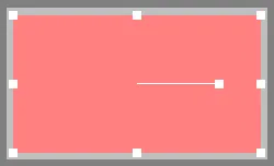
Example editing handles for a selected Fill object.
Click anywhere on an object away from editing handles (where they exist) to drag the object to reposition it. Depending on the type of object, it may be rotated and/or flipped while dragging.
-
Press Spacebar to rotate the object counterclockwise or Shift+Spacebar for clockwise rotation. Rotation is in accordance with the value for the Rotation Step defined on the PCB Editor – General page of the Preferences dialog.
-
Press the L key to flip the object to the other side of the board (where applicable).
-
Press the X or Y keys to flip the object along the X-axis or Y-axis where applicable.
-
Press the Alt key to constrain the direction of movement to the horizontal or vertical axis depending on the initial direction of movement.
-
Nudge the object by small amounts (according to the current snap grid value) by pressing the arrow keys while holding down the Ctrl key. Nudge by larger amounts (10 x snap grid value) pressing the arrow keys while holding down the Ctrl+Shift keys.
The number of primitives displayed when dragging multiple selected objects is controlled by the PCB.Rendering.MultiselectionDrag option in the Advanced Settings dialog (the default value is 500).
Movement Commands
Object position can be changed using commands of the Edit » Move sub-menu of the main menus or the movement sub-menu in the Active Bar.

-
Move - this command is used to move any object in the current document. Any nets associated to an object will remain connected and the connection lines will follow the object when it is moved (displayed or not in accordance with the connect mode in force). Any routed track connected to the object will not be moved.
-
Drag - this command is used to move any object in the current document. If the object has connected tracks and/or arcs (for example, a component, pad or via), these will remain connected as the object is moved.
-
For connected track to move with a component, the Comp Drag mode must be set to Connected Tracks on the PCB Editor - General page of the Preferences dialog. If this mode is set to None, the command behaves just like the basic move command.
-
When using this command to drag a component with the Comp Drag mode set to Connected Tracks, the rotate and flip key commands become unavailable. Also note that smart movement actions (dynamic alignment and pushing) also are not available.
-
Component - this command enables you to move components in the current document. After launching the command, click the component in the design that you want to move and move it to the required position then click. Alternatively, click within the design space away from any objects to open the Choose Component dialog. Use this dialog to locate the component you want to move (either by jumping to the component or having the component brought to the cursor) and then reposition in the same way as described above. Note that this feature will work only if the target component is not locked.
The command can also be accessed by right-clicking over a component in the design space then choosing the Component Actions » Move Component command from the context menu.
-
Move Selection - this command enables you to manually reposition selected objects on the current document. Any nets associated to an object in the selection will remain connected and the connection lines follow the object when it is moved (displayed or not in accordance with the connect mode in force). Any routed track connected to the object will not be moved.
-
Move Selection by X, Y - this command is used to offset the current selection of objects by a precise amount in X and/or Y directions. After launching the command, the Get X/Y Offsets dialog will open. Use this dialog to specify delta X and/or delta Y increment values by which to move the selection.
The command will only be available when at least one object is selected in the design space.

The Get X/Y Offsets dialog
Options and Controls of the Get X/Y Offsets Dialog
-
X Offset - use this field to specify the distance by which the selection should be moved along the horizontal axis. Positive and negative values can be specifed depending on the direction of movement required. Use the button to the right of this field to quickly toggle the entered value between positive or negative.
-
Y Offset - use this field to specify the distance by which the selection should be moved along the vertical axis. Positive and negative values can be specifed depending on the direction of movement required. Use the button to the right of this field to quickly toggle the entered value between positive or negative.
-
Toggle X/Y Offsets - click this button to quickly swap the offset values. The X Offset value will be used as the Y Offset value and vice versa.
-
Reset X/Y Offsets - click this button to quickly reset both offset values to zero.
-
Define X/Y Offsets Interactively - click this button to have the offsets calculated interactively. You will be taken to the workspace and prompted, in turn, to choose a start and end point. Click at the desired locations; the dX and dY values will be entered into the X Offset and Y Offset fields, respectively.
To switch the dialog units between imperial and metric, press the Ctrl+Q shortcut.
-
Rotate Selection - this command is used to rotate selected objects in the design space counterclockwise or clockwise and by a specified angle of rotation. After launching the command, the Rotation Angle (Degrees) dialog will open. Enter the required angle of rotation from 0.001° to 360.00° (resolution 0.001°). Enter a positive value for counterclockwise rotation or a negative value for clockwise rotation. Click OK to close the dialog then position the cursor and click to define the reference point for rotation. The selected objects will be rotated about the reference point by the entered angle.

The Rotation Angle dialog
-
Flip Selection - flip the selected object(s) horizontally (around the Y-axis) to the corresponding layer on the opposite side of the board. For example, objects on the Top Layer will be flipped to the Bottom Layer, objects on the Top Overlay will be flipped to the Bottom Overlay, etc.
-
The Designator and Comment text becomes mirrored after a flip action.
-
For a pad that exists on the Multi-Layer, flipping will essentially reverse the order of its XY size pairings and shapes. Therefore, if a style of Top-Middle-Bottom has been used and the shapes are initially Round-Rectangle-Octagonal, flipping will reverse the stack and thus the shapes from the top will become Octagonal-Rectangle-Round.
-
If there are multiple objects selected, the set of objects is flipped about the geometric center of the selection set.
Note that all selected objects are flipped without warning, unless one or more of the objects has its location locked. In that situation, a Confirm dialog will appear, requiring verification before the objects are flipped.
Alignment Commands
Objects can also be moved by changing their alignment. To align objects with other objects, right-click on a selected object, then select Align. Alternatively, use the Edit » Align sub-menu of the main menus or the alignment sub-menu in the Active Bar. The alignment sub-menu contains a number of options for distributing selected objects.
The alignment commands will only move selected objects that are free to move - locked objects will not be moved.

The Align command is used to access the Align Objects dialog, which provides controls for quickly aligning the set of currently selected design objects as required. Use the dialog to set options for both the Vertical and/or Horizontal alignment of the selected objects, as required, then click OK to effect alignment.

The Align Objects dialog
-
Enabling both Horizontal and Vertical options at the same time may result in a conflict with the selected objects becoming stacked on top of one another.
-
Using the Space equally options can result in the moving objects being off-grid.
Options and Controls of the Align Objects Dialog
-
Horizontal - choose from one of the following options to determine the horizontal alignment of the selected objects:
-
No Change - leave the horizontal alignment of the objects unchanged.
-
Left - align objects so the outer edge of their left-most primitives has the same X location. The object with the left-most primitive is used as the reference.
-
Center - move objects horizontally so their centers are aligned. After clicking OK, you are prompted to click to choose the reference object.
-
Right - align objects so the outer edge of their right-most primitives has the same X location. The object with the right-most primitive is used as the reference.
-
Space equally - objects are equally spaced in the horizontal direction, between the left-most and right-most objects (which do not move).
-
Vertical - choose from one of the following options to determine the vertical alignment of the selected objects:
-
No Change - leave the vertical alignment of the selected objects unchanged.
-
Top - align objects so the outer edge of their upper-most primitives has the same Y location. The object with the upper-most primitive is used as the reference.
-
Center - move objects vertically so their centers are aligned. After clicking OK, you are prompted to click to choose the reference object.
-
Bottom - align objects so the outer edge of their lower-most primitives has the same Y location. The object with the lower-most primitive is used as the reference.
-
Space equally - objects are equally spaced apart in the vertical direction, between the upper-most and lower-most objects (which do not move).
The Position Component Text command is used to run the Component Text Position dialog from where you can change the position of the designator and/or comment text for one or more selected components in the current document.

The Component Text Position dialog
The dialog is essentially divided into two regions - the Designator and Comment text. For both designator and comment, a graphical representation of a component is used as an aid to show where the text will appear based on the position selected. The following nine positional styles are available for the text, all of which are classed as 'automatic positions', meaning the text remains in the chosen position as the component is moved and rotated:
-
Left-Above
-
Left-Center
-
Left-Below
-
Center-Above
-
Center
-
Center-Below
-
Right-Above
-
Right-Center
-
Right-Below
To leave text in its current position with no modification, leave the No Change option enabled.
-
The designator and comment text positions can also be changed through the Properties section of the Properties panel. Select the designator/comment or the parent component to have these properties displayed. Click the relevant control that textually summarizes the current layer, position and rotation for the designator/comment then use the Autoposition property available in the pop-up window, as required.
-
To freely position the designator/comment text and have it follow the parent component's movement/orientation, choose the Manual style for the Autoposition property (when configuring properties through the Properties panel). You also can freely click, hold and drag text to the required position directly in the workspace; this will automatically switch the Autoposition property to Manual.
The Align Left / Align Right / Align Top / Align Bottom command enables you to align selected design objects by their left/right/top/bottom edges, respectively. After launching the command, the left/right/top/bottom edge of the left/right/top/bottom-most object is used as a reference, and all other objects in the selection will be moved left/right/top/bottom, so that their left edges are aligned with this reference.
The Align Left (maintain spacing) / Align Right (maintain spacing) / Align Top (maintain spacing) / Align Bottom (maintain spacing) command enables you to align selected design objects by their left/right/top/bottom edges while maintaining adequate spacing in observance with applicable design rules. After launching the command, the left/right/top/bottom edge of the left/right/top/bottom-most object is used as a reference, and all other objects in the selection will be moved left/right/top/bottom, so that their left edges are aligned with this reference. An object will be moved left/right/top/bottom as close to the reference object as the applicable clearance rule allows:
The Align Horizontal Centers / Align Vertical Centers command enables you to place selected objects in a single column/row, aligned by their horizontal/vertical centers. After launching the command, the cursor will change to a cross-hair and you will be prompted to select one of the objects in the selection; click on it. This becomes the reference object. All other objects in the selection will be moved in relation to this reference object, aligned by their horizontal/vertical centers.
The Distribute Horizontally / Distribute Vertically command allows you to make the horizontal/vertical spacing of a selection of objects equal. After launching the command, the left-most and right-most / top-most and bottom-most objects in the selection will remain fixed in their positions with all other objects spaced equally between them. The vertical/horizontal position of the objects is not changed.
The Increase Horizontal Spacing / Increase Vertical Spacing command allows you to increase the horizontal/vertical spacing of a selection of objects. After launching the command, the left-most/bottom-most object will remain fixed while the other objects in the selection will be moved right/up. Movement is such that the horizontal/vertical distance between the reference points of consecutive objects is increased by the amount specified in the Step X / Step Y field for the default Global Board Snap Grid.
The Decrease Horizontal Spacing / Decrease Vertical Spacing command allows you to decrease the horizontal/vertical spacing of a selection of objects. After launching the command, the left-most/bottom-most object will remain fixed while the other objects in the selection will be moved left/down. Movement is such that the horizontal/vertical distance between the reference points of consecutive objects is decreased by the amount specified in the Step X / Step Y field for the default Global Board Snap Grid.
The Align To Grid command is used to move selected components to the nearest point on the applicable and modified snap grid. After launching the command, the reference points for each of the selected components will be moved to the nearest point on the applicable snap grid.
The Move All Components Origin To Grid command is used to move the reference point of all components onto the current Snap Grid. After launching the command, all components in the design space whose pads are on-grid will be moved so that their reference points are aligned to the current snap grid. By default, a report - Move Component(s) Origin To Grid - <PCBDocumentName>.html - will automatically be generated and opened as the active document detailing which components have and have not been moved.
-
Configure which format of report(s) to generate and show from the PCB Editor - Reports page of the Preferences dialog.
-
The applicable snap grid can be set up as required through the Grid Manager section of the Properties panel.
Note that components whose pads are currently off-grid are not moved.
Via the PCB List Panel
The PCB List panel allows you to display design objects in tabular format, enabling quick inspection and modification of object attributes. When used in conjunction with the PCB Filter panel, it enables you to display just those objects falling under the scope of the active filter – allowing the targeting and editing of multiple design objects with greater accuracy and efficiency.
Selecting the Active Layer
The active layer is the layer you will be placing objects on. The active layer can be selected from currently visible layers by clicking the tab for this layer at the bottom of the design space or using the Active Layer drop-down in the Layers region of the Layers & Colors tab of the View Configuration panel.
You can also use the following shortcuts to quickly select the active layer:
-
* (on numeric keypad) – switch to the next enabled signal layer.
-
Shift+* (on numeric keypad) – switch to the previous enabled signal layer.
Note that this command is only available with the editor in 2D viewing mode, since in 3D mode the Shift key is used to access the directional sphere.
-
+ (on numeric keypad) – switch to the next enabled layer.
-
- (on numeric keypad) – switch to the previous enabled layer.
Objects placed on the multi-layer automatically appear on all signal layers.
Using Cut/Copy and Paste
In the PCB editor, you can cut/copy and paste objects within or between PCB documents, e.g., component(s) from a PCB can be copied into another PCB document. You can cut/copy objects to the Windows clipboard and paste them into other documents.
When using 2D Layout Mode, select the object(s) you want to cut/copy, click Edit » Cut (Ctrl+X) / Edit » Copy (Ctrl+C) from the main menus or choose the Cut/Copy command from the right-click menu. The cursor will change to a crosshair and you will be prompted to select a reference point. This is a coordinate relative to the selected object(s) and is used to accurately position the selection when using the paste command.
When using the Copy command in 3D Layout Mode, the current view in the design space will be copied to the clipboard in bitmap format. You have control over the resolution of the copied image via the 3D Snapshot Resolution dialog that subsequently opens.
To copy the currently selected design object(s) to the clipboard in textual format, the Edit » Copy As Text command from the main menus can be used. This information can then be pasted into any text field or external text document. The details copied to the clipboard include:
-
The type of object it is.
-
The designator and comment (for a component object).
-
The object's location in the design space.
-
The layer upon which the object resides (or start and stop layers for a via).
An example of a component copied as text to the clipboard is:
Component Y1-25MHz (100.6mm,1.5mm) on Top Layer
An example of a track and via copied as text to the clipboard is:
Track (20mm,6mm)(80mm,6mm) Top Layer
Via (45mm,6mm) Top Layer to Bottom Layer
To place the last content cut/copied to the clipboard, into the active document, choose the Edit » Paste command from the main menus or right-click within the design space and choose the Paste command from the context menu (shortcut: Ctrl+V). The latest clipboard content will appear floating on the cursor. The cursor position relative to the content is determined by the reference point designated when Cut or Copy was used to add the selection to the clipboard.
When using the Paste command, objects are pasted onto the same layer that the source objects were copied from regardless of which layer is currently set as the active layer in the editor.
To place the text that has been copied from a supported OLE application into any open PCB document, the Edit » Paste Text command from the main menus can be used. The text is converted to, and pasted as, PCB string objects rather than a single OLE object. The supported file types include universal formats such as CSV and XLS format spreadsheets and DOC and RTF word documents.
To control what happens to certain object attributes when they are pasted back into the design space, the Edit » Paste Special command from the main menus can be used. After launching the command, the Paste Special dialog will open.

The Paste Special dialog
Options and Controls of the Paste Special Dialog
Paste Attributes
-
Paste on current layer - enable this option to paste objects onto the current layer.
-
Keep net name - enable this option to keep the original net names for the objects.
-
Duplicate designator - enable this option to paste a component with the same designator without auto-incrementing.
-
Add to component class - enable this option to have the pasted component added to the same component class as the source component.
The Duplicate designator and Add to component class options become available for use when the copied source component is available on the clipboard.
Buttons
-
Paste - click to paste the object with all specified attributes.
-
Paste Array - click to open the Setup Paste Array dialog in which you can set up options for array paste.
Depending on the specific content being pasted, the following attributes can be controlled:
Setup the options as required then click the Paste button to start the paste operation.
Clicking the Paste Array button in the Paste Special dialog will open the Setup Paste Array dialog, which allows you to paste multiple copies of the clipboard objects into the current document.

The Setup Paste Array dialog
Options and Controls of the Setup Paste Array Dialog
Placement Variables
-
Item Count - the number of repeat placements to be performed. For example, typing 4 will place 4 copies of the current clipboard contents.
-
Text Increment - enter the automatic increment for the display text (e.g., component or pad designator). Both alpha and numeric increments other than 1 are supported. For example, by setting the designator of a pad prior to copying it to the clipboard and setting the Text Increment field, the following types of pad designator sequences can be placed:
-
Numeric (1, 3, 5)
-
Alphabetic (A, B, C)
-
Combination of alpha and numeric (A1, A2, or 1A, 1B, or A1, B1 or 1A, 2A, etc)
-
To increment numerically, set the Text Increment field to the amount you wish to increment by.
-
To increment alphabetically, set the Text Increment field to the letter in the alphabet that represents the number of letters you wish to skip. For example, if the initial pad had a designator of 1A and the Text Increment field was set to C (the third letter of the alphabet), the pads would have the designators 1A, 1D (three letters after A), 1G (three letters after D), and so on.
-
Note that the last-used incremental value is remembered after pasting an array, the next value in that sequence will be used as the base value of the next array that you paste, unless you perform a new Copy action.
Array Type
-
Circular- enable this option to paste a circular array, using the current Circular Array settings.
-
Linear - enable this option to paste the array in a straight line, using the current Linear Array settings.
Circular Array
-
Rotate Item to Match - if enabled, array items will be rotated by the same angular amount as their Spacing.
-
Spacing (degrees) - the angular space between two adjacent pasted items.
Linear Array
-
X-Spacing - enter the desired X space between two adjacent items.
-
Y- Spacing - enter the desired Y space between two adjacent items.
When you paste the array, it will be held by the same reference location that was used when the Copy action was performed.
Enter the appropriate values in this dialog then click OK to place the array.
-
If placing a linear array, you will be prompted to select the starting point for the array. Position the cursor then click or press Enter to place the array.
-
If placing a circular array, you will be prompted to select the center point for the array, followed by the starting point for the array. Position the cursor in each case then click or press Enter to place the array. The objects will be placed in counterclockwise fashion around the nominated center point.
The starting point for the array will be where the reference point - designated when Cut or Copy was used to add the selection to the clipboard - will be located. It is therefore advisable to ensure the reference point is properly designated at the time of cut/copy, otherwise unexpected results may occur when pasting the array.
To copy one or more selected objects and then paste multiple instances of the selection wherever required in the current document, you can also use the Edit » Duplicate command from the main menus (shortcut: Ctrl+R). After launching the command, the cursor will change to a cross-hair and you will enter duplicate mode. The process involves the following sequence of steps:
-
You will first be prompted to select a reference point. This is the point by which the selection will be pasted. Move the cursor to the required position near to the selection then click or press Enter. A copy of the selection will appear floating on the cursor.
-
Move the cursor to the desired location in the design space then click or press Enter to place the copy.
-
Another copy of the selection will appear floating on the cursor ready for placement.
-
Continue placing further instances of the copied selection (rather like using a rubber stamp) or right-click or press Esc to exit.
Note that this command is used to copy and paste objects. As such, you cannot use the command for duplicating the children of group objects.
Priorities When Pasting Objects
When an object is being pasted on a copper layer and it overlaps a set of objects of different types when pasted, a net of the highest priority object will be assigned to the pasted object. The priorities are as follows (1 is the highest priority):
-
Pad
-
Fill
-
Region
-
Track
-
Arc
-
Via
-
Polygon Pour
 pasted over a set of objects of different types with different nets assigned. Since the pad is the object of highest priority in this set, its net (Pad_Net) will be assigned to the pasted object. Hover the cursor over the image to see the result.")
A net of the highest priority object is assigned to a pasted object. Here is shown an object (track) pasted over a set of objects of different types with different nets assigned. Since the pad is the object of highest priority in this set, its net (Pad_Net) will be assigned to the pasted object. Hover the cursor over the image to see the result.
When an object is being pasted on a copper layer, and it overlaps a set of objects of the same type when pasted, a net of the object that is under the cursor when clicking to paste the object will be assigned.
 pasted over a set of objects of the same type (pads). Since pad 2 is the object that is under the cursor when clicking to paste the object, the net of this pad (Pad2_Net) will be assigned to the pasted object. Hover the cursor over the image to see the result.")
A net of the object under the cursor is assigned to a pasted object. Here is shown an object (track) pasted over a set of objects of the same type (pads). Since pad 2 is the object that is under the cursor when clicking to paste the object, the net of this pad (Pad2_Net) will be assigned to the pasted object. Hover the cursor over the image to see the result.
When a set of physically connected objects is being pasted on a copper layer, and objects of different types in this set overlap existing objects with different nets, a net of the highest priority object in this set will be assigned to all pasted objects. The above priorities are applied in this case.
 pasted over objects (vias) with different nets assigned. Since the fill is the object of highest priority in this pasted set, the net assigned to it (Via1_Net) will be assigned to each object in this set. Hover the cursor over the image to see the result.")
The net assigned to the highest priority object is assigned to the set of physically connected objects. Here is shown a set of connected objects (from left to right: Fill, Region, Track, Arc, Via, Polygon Pour) pasted over objects (vias) with different nets assigned. Since the fill is the object of highest priority in this pasted set, the net assigned to it (Via1_Net) will be assigned to each object in this set. Hover the cursor over the image to see the result.
Locking Design Objects
Design objects can be locked from being moved or being edited on the PCB document by enabling their Locked attributes. For instance, if the position or size of specific objects is critical, lock them. Locking can be done in the Properties panel by clicking on the padlock icon ( ) for the desired object(s) as shown in the following examples.

Examples of the Lock icon in the Properties panel for a selected component and pad.
To toggle the state of the Locked property for a placed object that has the Locked property, you can also right-click over the object in the design space and choose the <ObjectType> Locked command from the context menu. When the object is already locked, the command entry on the menu will display a tick icon to the left.
If you attempt to move or rotate a design object that has its Locked property enabled, a dialog appears asking for confirmation to proceed with the edit.
If the Protect Locked Objects option is enabled in the PCB Editor – General page of the Preferences dialog and the design object is locked, the object cannot be selected or graphically edited. Use the Lock icon on the Properties panel to unlock the object or disable the Protect Locked Objects option to graphically edit this object.
If you attempt to select locked objects along with other objects, only those objects that are unlocked can be selected and moved as a group when the Protect Locked Objects option is enabled.
Component Primitive Locking
If a PCB component has its primitives locked (the Primitives option in the Component mode of the Properties panel is in its  state), all or the most properties of these primitives cannot be modified using graphical (e.g., using drag-and-drop) and non-graphical (e.g., using the Properties or List panel) editing methods. This will help to prevent occasional changes of component primitives that can result in incorrect assembly and fabrication outputs.
To enable/disable the preventing modification of PCB component primitives functionality, use the
Protect Locked Primitives In Component option on the
PCB Editor – General page of the
Preferences dialog.
By way of an example, the Pad mode of the Properties panel is shown in the image below for a pad that is a constituent part of a PCB component that has its primitives locked. Note that all properties of the pad (except for Net and Testpoint properties) are dimmed and not available for editing. Note also that the  icon is shown at the far right of the pad's Component field, which denotes that the parent component has its primitives locked, and pad properties cannot be modified.
 for a pad of a PCB component that has its primitives locked (on the right).")
The Pad mode of the Properties panel (on the left) for a pad of a PCB component that has its primitives locked (on the right).
Re-Entrant Editing
The PCB Editor includes a powerful feature called re-entrant editing. This allows a second operation to be executed using keyboard shortcuts without the current operation being terminated. Re-entrant editing allows you to work more flexibly and intuitively. For example, consider starting to place a track and then realizing that another track segment must be deleted. There is no need to drop out of Interactive Routing mode. Press the E, D shortcut keys, delete the required track segment then press the Esc key to return to interactively routing the design.
Setting the PCB Cursor Appearance
By default, the PCB cursor is set as a small green 90 degree cross. This can be configured using the Cursor Type and Cursor Color settings, on the PCB Editor – General page of the Preferences dialog. For example, a large 90 degree cross that extends to the edges of the design window (Large 90 option) can be useful when placing and aligning design objects. Alternatively, a cross at 45 degrees (Small 45 option) might be useful if the 90 degree options are hard to see against grid lines.
True Type Font Support
The PCB Editor offers the ability to use Stroke-based or TrueType fonts for text-related objects in a design (text strings/frames, dimensions, drill tables, and/or layer stack tables). Choice of font is made from within the associated Properties panel. Three Stroke-based font options are available - Default, Sans Serif, and Serif. The Default style is a simple vector font that supports pen plotting and vector photoplotting. The Sans Serif and Serif fonts are more complex and will slow down vector output generation, such as Gerber. The Stroke-based fonts are built into the software and cannot be changed. All three fonts have the full IBM extended ASCII character set that supports English and other European languages. When using TrueType fonts, TrueType and OpenType (a superset of TrueType) fonts found in the \Windows\Fonts folder are available for use. The feature also offers full Unicode support.
Note that only detected (and uniquely named) root fonts will be available for use. For example, Arial and Arial Black will be available but Arial Bold and Arial Bold Italic will not.
Geometries of text objects using TrueType fonts are automatically stored inside PCB documents. When objects in a PCB document use a TrueType font, these objects will be shown using the same font geometry when the PCB document is opened on another computer, even if that TrueType font is not installed.
When an object that uses a missing font is selected, a warning message appears at the top of the Properties panel. When changing object properties that affect its text (e.g., the text height or text itself), the Missing fonts dialog opens in which you can select a replacement font (Replacement). Enable the Apply to all text elements option to apply the replacement font to all objects in the PCB document using the missing font.

The dialog also appears when changing text-related properties from the PCB List panel.
When trying to edit multiple objects using different missing fonts, the dialog allows you to select a replacement for each missing font.

The ability to automatically store geometries of text objects that use TrueType fonts inside PCB documents is available when the PCB.Text.TTFontSaving option is enabled in the Advanced Settings dialog. When the option is disabled, you can configure Altium Designer to embed TrueType fonts. The PCB Editor – TrueType Fonts page of the Preferences dialog (available when the PCB.Text.TTFontSetting.Hide option is disabled in the Advanced Settings dialog) provides the Embed TrueType fonts inside PCB documents option for embedding TrueType fonts when saving a design and the Substitution font option for applying the chosen font substitution when loading a design.
Embedding fonts is useful when text is required to be displayed in a font that may or may not be available on a target computer upon which the design is loaded. Font substitution enables specification of a TrueType font to be used as a replacement when loading a design where fonts have not been embedded and fonts may not be available on the computer upon which the design is currently loaded.
Net Information
For copper objects on a PCB (track, via, polygon, etc.), the following information is presented in the Net Information region of the Properties panel when the object is selected:
-
The parent Net, Diff Pair and/or xSignal and associated class in each case. Note that the Diff Pair and xSignal entries are shown only if the object is a part of a differential pair or xSignal, respectively.
-
Delay – the delay of the selected object(s) and the delay of the routed segments of the entire net. Include the Propagation Delay values of pads and vias, if they have been defined for the pads and vias.
For vias, the propagation delay is calculated in proportion to the length of the via used. This feature is available when the PCB.Delay.Via option is enabled in the Advanced Settings dialog. When the PCB.Delay.Via option is disabled, the Propagation Delay value defined in via properties is used.
-
Length – the total length sum of the selected object(s) and the total Signal Length. The Signal Length is the accurate calculation of the total node-to-node distance. Placed objects are analyzed to: resolve stacked or overlapping objects and wandering paths within pads; and via lengths are included. The Pin Package Length is also included if it has been defined for the pad(s). If the net is not completely routed, the Manhattan (X + Y) length of the connection line is also included. For more information regarding Signal Length and its applications, see the information about the PCB - Nets panel.
-
The total length includes an estimate for the unrouted part of the net (the Manhattan (X + Y) length of the connection line), but for the total delay, it does not.
-
The Delay and Length for a net that is part of a defined Supply Nets design rule (or part of a net class used with such a rule) is not calculated.
-
Max Current - the maximum current that the selected Track, Arc or Via object(s) can carry, determined from the IPC-2221A formula (Section 6.2):
I = k * ΔT0.44 * A0.725
where:
I = current [amps]
A = cross-sectional area [sq mils] (trace width * layer stack copper thickness, or Abarrel, as shown below)
ΔT = allowable temperature rise above ambient [°C]
k = constant, such that:
k = 0.048 for outer layers
k = 0.024 for inner layers
When multiple objects are selected, for example an entire net, the Max Current for that net is the smallest individual Max Current value of the selected objects.
-
Resistance - the sum of the resistance of the selected Track, Arc and Via objects, determined from the derived formula:
R = (ρ * L / A)
where:
R = resistance [Ω]
ρ = resistivity of copper [Ω*mm2/m]
L = trace length [m] (or Via Length, as described below)
A = cross-sectional area = T * W [mm2] (or Abarrel, as shown below)
T = trace thickness (from layerstack) [mm]
W = Trace width [mm]
Assumptions:
-
Ambient temperature = 22 °C
-
Allowable temperature rise = 20 °C
-
Thruhole copper wall thickness = 0.018mm
-
Resistivity of copper = 0.017 Ω*mm2/m
The total Resistance of the selected objects is the sum of the resistance of the individual objects.
Via Barrel Cross-Sectional Area - determined as follows:

Abarrel = AViaHoleSize - AFinishedHoleSize
Abarrel = [ π * (ViaHoleSize/2)2 ] - [ π * ((ViaHoleSize - 2 * ViaWallThickness)/2)2 ]
Abarrel = π (ViaHoleSize * ViaWallThickness - ViaWallThickness2)
Via Length = distance from the center of entrance layer to the center of exit layer, as shown above
Notes - via length in these calculations is dependent on the via belonging to a net and the layers used by the connected tracks. A selected via with no net assigned will display the layer-edge to layer-edge length instead of the layer-center to layer-center length. Also, a via with a net assigned but no connected tracks will display a length of zero.

The Net Information region of the Properties panel. Shown here is an example for a selected track.
Click a link in the Net Information region to open the associated net/differential pair/xSignal in the PCB panel.
Assigning Nets to Objects
The PCB editor provides a number of ways to assign nets to primitive objects:
-
When one or more objects are selected, use the drop-down of the Nets field in the Properties panel. All nets for the active board design will be listed in the drop-down list. Select No Net to specify that the track is not connected to any net. Alternatively, you can click on the Assign Net icon (
 ) to choose an object in the design space - the net of that object will be assigned to selected objects.
-
Right-click over one or more selected objects, then choose Net Actions » Assign Net. After launching the command, a crosshair appears. Hover the cross-hair to the net to which you want to assign the object(s), then click to select that net.
-
To resynchronize the net name of the routing primitives to the net name on the pads to which they connect, select the Design » Netlist » Update Free Primitives From Component Pads command from the main menus. After launching the command, a confirmation dialog opens asking whether you want to update free primitive nets with the component-pad nets. After clicking Yes and starting from each pad, the connected copper is selected and the net name of each primitive is set to match that of the pad. This operation does not affect the internal PCB netlist.
To examine and confirm that the objects that are physically connected, have the correct net assigned to belong in that physical net (a physical net means connected copper in this instance), you can use the Configure Physical Nets dialog accessed by choosing the Design » Netlist » Configure Physical Nets command from the main menus. The software analyzes the design, checking that all pads and the objects that physically connect them together (tracks, arcs, fills, etc.,) have the same net name assigned. When all net objects are correct, the net is shown in green. If any objects are detected as touching but have a different net assigned, they are flagged in red. A common example of when this can occur is if a component footprint has extra copper objects within the footprint. When this footprint is loaded during synchronization, the pads have the assigned net name applied to each pad but not the extra copper. The dialog is interactive; click on a net or primitive to cross probe to that object. Right-click or click the Menu button to access the available commands. The Action region of the dialog provides controls for specifying the action needed to be taken to resolve issues with the connected copper. By default, actions will be set automatically but can be adjusted as required. Once the actions are set, click the Execute button to update the net assignments.
Note that the default state for this dialog is to Only Show Errors, which means that objects that are correctly assigned are not listed. Disable this option by disabling the Only Show Errors option (using the Menu button) in order to display all objects using the Menu button.
 and Only Show Errors option disabled (front)).")
The Configure Physical Nets dialog (displaying Only Show Errors option enable (back) and Only Show Errors option disabled (front)).
Options and Controls of the Configure Physical Nets Dialog
-
Electrically Connected Copper - this region lists distinct groupings of copper primitives that are electrically connected as detected in the wiring of the design. For each grouping, the following information is presented:
-
Primitive - at the top-level, this entry reflects how many primitives are in the connected copper. Primitives can be displayed in a flat listing or grouped by type of primitive. The latter is configured by enabling the Show Primitive Groups option of the Menu button options. If this is done, the primitives will be split into the following groupings:
-
Connected Component Primitives - lists all component pad primitives as its children. These can be further grouped by parent component by enabling the Menu button option Show Components.
-
Connected Free Primitives - lists all non-component copper primitives as its children, further grouped by primitive type (Fills, Polygons, Tracks, Vias).
Connected Component Primitives are only presented when the Show Component Pads option is enabled on the Menu button options. Similarly, Connected Free Primitives are only presented when the Show Non Component Pads option is enabled. If one of these options is disabled, the top-level entry will reflect how many primitives are currently hidden. If both of these options are disabled, the dialog will be empty! The Show All Primitives button will become available at the bottom of the dialog, which quickly reveals all primitives (essentially enabling one or both of these disabled options).
Clicking on a primitive entry will highlight that primitive in the design space. Selecting multiple primitive entries will select all primitives in that selection. Selecting a higher-level entry in the list will cause all descendent child primitives to be highlighted in the workspace.
-
Original Net Names - this field reflects the net name currently assigned to the primitive, i.e., the net to which the primitive currently connects. The entry will be one of the defined nets for the board. However, if a primitive is not connected to a net, it will have the entry <Unassigned>.
-
Status - this field provides a top-level status entry for the grouping, which can be one of four states:
-
Blank - net assignment for the connected copper grouping is all correct and no update is required. The top-level entry for the grouping is colored green.
-
1. Update Required - Unassigned Nets - in this state, none of the primitives in the grouping have been assigned to a net. The top-level entry for the grouping is colored yellow.
-
2. Update Required - Some Unassigned Nets - in this state, some of the primitives have been assigned to the same net, but others have not been assigned at all. The top-level entry for the grouping is colored orange.
-
3. Ambiguous - Multiple Net Names - in this state, there are primitives in the grouping that have been assigned to different nets. There may also be primitives not yet assigned. The top-level entry for the grouping is colored red.
-
Action - this region provides controls for specifying the action needed to be taken to resolve issues with the connected copper along with the result of executing the configured changes. For each grouping, the following is presented:
-
Proposed Action - this field is used to determine what action, if any, is to be taken. At the highest level for a grouping, this entry can be set to Update Net To, or Don't Update Net To. When updating, choose the new target net in the New Net Name field. Based on these two settings, the software calculates the actions that are to be performed at the child primitive level, arriving at one of the following proposals:
-
No Action Required - the primitive is already assigned/connected to the target net.
-
Update - include the primitive in the update so that it is assigned/connected to the new target net.
-
Don't Update - do not include the primitive in the update. It will remain connected to its current net.
-
New Net Name - use this field to set a new target net to which the primitives should be connected. The field's drop-down lists all nets detected among the primitives in the connected copper grouping. If you need to use a different net, right-click on the field and use the Change Copper Net To Board Net command from the context menu. This opens the Choose Net dialog which lists all nets currently defined for the board. Choose the net you require then click OK. That net will be entered into the field.
-
Done - this field reflects the success (
 ) or failure (
 ) of the update action once the Execute button is pressed and the changes applied.
Toggling the proposed action at a parent level quickly toggles the proposed action at the child level and for all children under that parent. Where individual children differ in their proposed actions - some included for update, some excluded - the parent level above in the hierarchy of grouped primitives will reflect this with the entry Some Updates.
-
Execute - once you are satisfied with the actions assigned to the netlist, click this button to update the net assignments.
-
Menu - click to access the following menu of commands that relate to the main list in general or to the currently selected primitive(s). The commands are identical to those available on the right-click menu for the main list region.
-
Update/Don't Update/No Action - use to quickly toggle the proposed action for the selected primitive(s). At a higher, parent level in the primitive hierarchy, use it to toggle the proposed action for all descendent children.
-
Select All - use to quickly select all connected copper groupings (the highest level entries in the list).
-
Select All With Same Status - with a top-level connected copper grouping entry selected, use this command to quickly select all other top level groupings with the same status.
-
Clear All Selected - use to deselect all entries in the list.
-
Expand All In Connected Copper - use to quickly expand all child groupings within the currently focused connected copper grouping.
-
Expand All - use to quickly expand all groupings for all connected copper groupings in the list.
-
Expand Children - use to quickly expand all descendent child groups below the currently selected grouping.
-
Collapse All In Connected Copper - use to quickly collapse all child groupings within the currently focused connected copper grouping.
-
Collapse All - use to quickly collapse all groupings for all connected copper groupings in the list.
-
Collapse Children - use to quickly collapse all descendent child groups below the currently selected grouping.
-
Only Show Errors - enable to only show errors in the dialog. The list will only present connected copper groupings whose Status is level 1, 2, or 3. Disable to also show connected copper that is correctly assigned.
-
Show Components - enable to have component pad primitives grouped by their parent components.
-
Show Primitive Groups - enable to have primitives grouped by their primitive type.
-
Animate Action Execution - enable to have the dialog scroll through the list as the execution proceeds, giving you an animated real-time progress of the execution of net changes. Disabling this option means execution of changes will be performed without such animation.
-
Warn On Netlist Change - enable to be warned when changes will affect the netlist for the board. The Netlist Change dialog will open, alerting you to how many primitives will have their nets changed and that this will affect the netlist. You can either click to Continue or click Filter Affected to more closely inspect the proposed changes.

The Netlist Change dialog
-
Show Component Pads - enable to show connected component primitives in the list.
-
Show Non Component Pads - enable to show connected free primitives in the list.
-
Show Changes That Affect Netlist - enable to only present a list of the proposed actions (changes) that will affect the netlist for the board.
-
Change Copper Net To - one or more menu entries of this type appear when there are not many nets currently assigned to primitives within the focused connected copper grouping. Use such an entry to quickly choose the target net for the New Net Name field.
-
Change Copper Net To Net - this menu entry appears when there are too many nets currently assigned to primitives within a connected copper grouping to display as individual menu entries. Using this command gives access to the Choose Net dialog, listing all nets currently assigned to primitives within the grouping. Choose the net you require then click OK; that net will be entered into the New Net Name field for the focused connected copper grouping.
-
Change Copper Net To Board Net - use this command if you need to use a different net to those currently assigned to primitives of the focused connected copper grouping. This opens the Choose Net dialog, listing all nets currently defined for the board. Choose the net you require then click OK; that net will be entered into the New Net Name field.
-
Show All Primitives - click this button to quickly reveal all primitives. This button becomes available if the Show Component Pads and/or Show Non Component Pads options are disabled on the menu.
You can also clear all nets from the current design document, essentially flushing the internal PCB netlist. This may be desirable if you have changed net information in the source schematic documents and you want to fully resynchronize your PCB with the source schematic netlist information. To do this, choose the Design » Netlist » Clear All Nets command from the main menus. After launching the command, a confirmation dialog will open alerting you to the fact that this operation will clear all net information from the PCB. After clicking Yes, all net information will be removed. Any routed track will remain routed but will have a No Net assignment. Any unrouted logical connections will be removed.
To create a netlist file based on the connectivity created by the routing in the current design, choose the Design » Netlist » Create Netlist From Connected Copper command from the main menus. After clicking Yes in the confirmation dialog that opens, a netlist (Generated <PCBDocumentName>.Net, added to the Projects panel as a free document under the Source Documents sub-folder) is created in the same folder as the PCB design document and automatically opened as the active document. Each net in the netlist gets its name from one of the pads to which the routed copper connects.
