UPCOMING HIGHLIGHT
Wire Bonding 3D Enhancements
The Wire Bonding 3D enhancements expand the ability to accurately model, visualize, and validate bond wires within advanced packages and assemblies. It introduces refined shaping controls, bonding type selection (Ball–Wedge and Wedge–Wedge), color overrides, expanded 3D body support, clearance checking inclusion, and improved filtering and documentation options. Together, these capabilities provide greater modeling precision, clearer manufacturing communication, earlier mechanical issue detection, and more controlled, professional documentation outputs. Available in Open Beta.
Explore additional upcoming features
See what we're working on, get an insight into what's going on below the
surface and which features you'll be able to take advantage of soon.
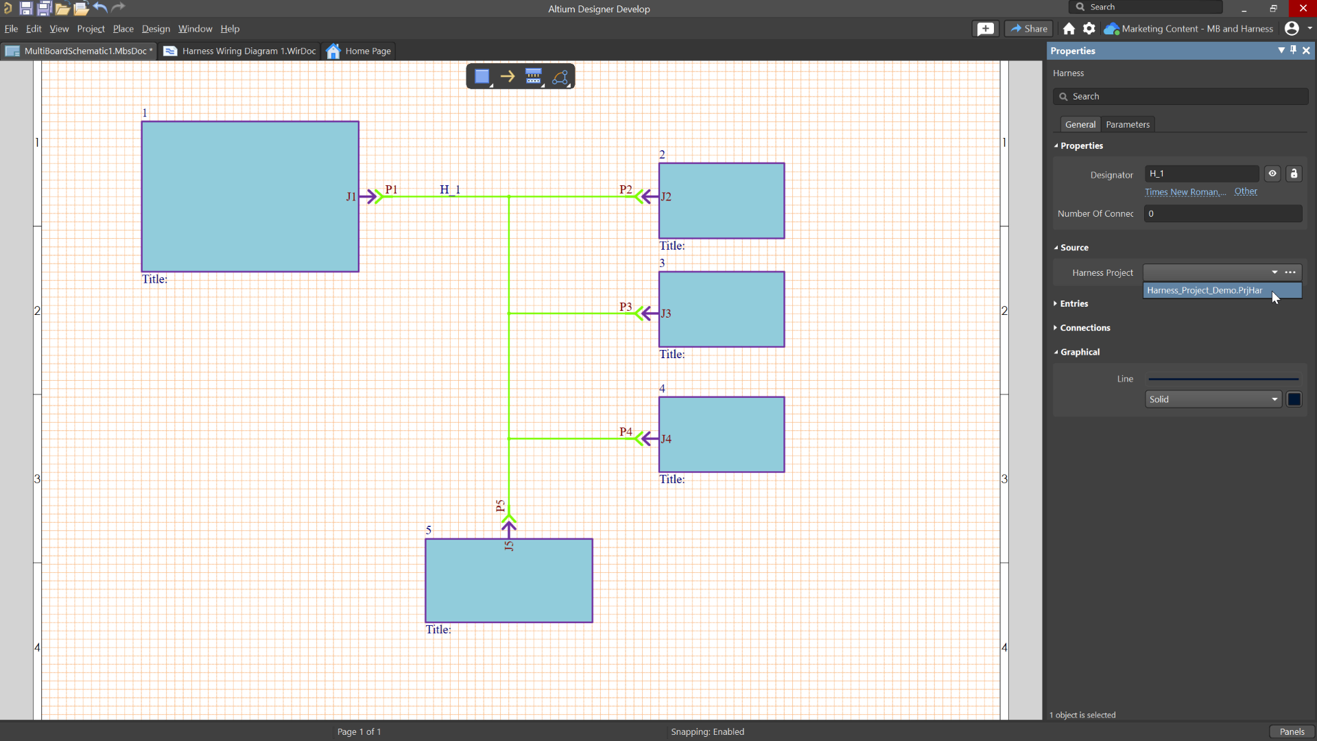
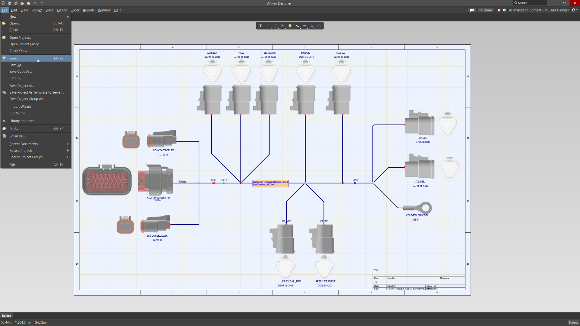
Selectable Harness Source Within Multi-board Design
 Available in Closed Beta

Selectable Harness Source Within Multi-board Design allows to select a harness design project as the source for a harness connection and supports bidirectional synchronization between the multi-board schematic and harness wiring diagram, making it easier to manage and maintain harness connectivity across a system.
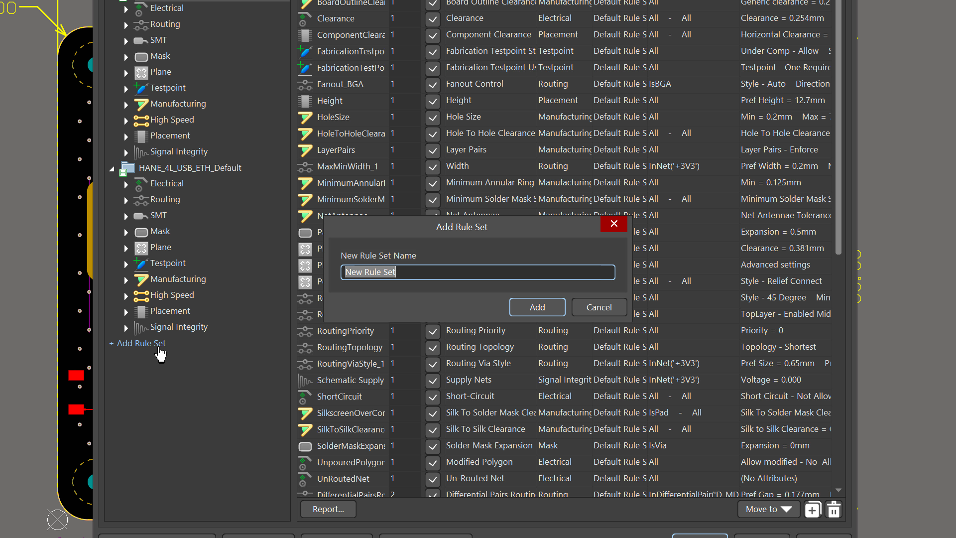
Design Rule Sets
Available in Closed Beta
PCB design rules can now be organized into reusable Rule Sets within the PCB Rules and Constraints Editor. Rule sets can be created, duplicated, enabled or disabled, renamed, deleted, imported, and exported, making it easier to manage rules for specific interfaces, manufacturers, or design requirements. Rule priority behavior remains unchanged, with the highest-priority applicable rule still taking precedence across all enabled rule sets. Batch DRC, rule violation panels, messages, and verification reports now include rule set information, with backward compatibility for older projects.
Interactive Dynamic Phase Tuning
Available in Closed Beta
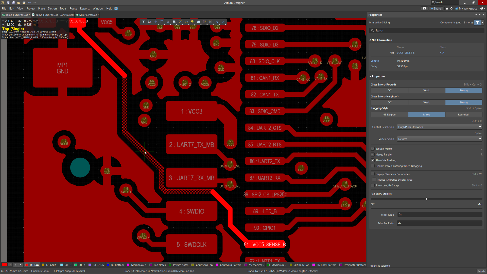
The Interactive Length Tuning tool lets you manually tune one net in a differential pair while equalizing pair length and maintaining phase alignment across the full route. This feature extends rule-driven interactive length tuning by using the applicable Matched Lengths rule, including Within Differential Pair Length and Dynamic Phase Matching settings, to guide pattern generation as you build the tuning pattern. The result is more efficient differential signal transmission, greater control during manual tuning, and faster creation of tuning patterns that stay within defined phase tolerance targets.
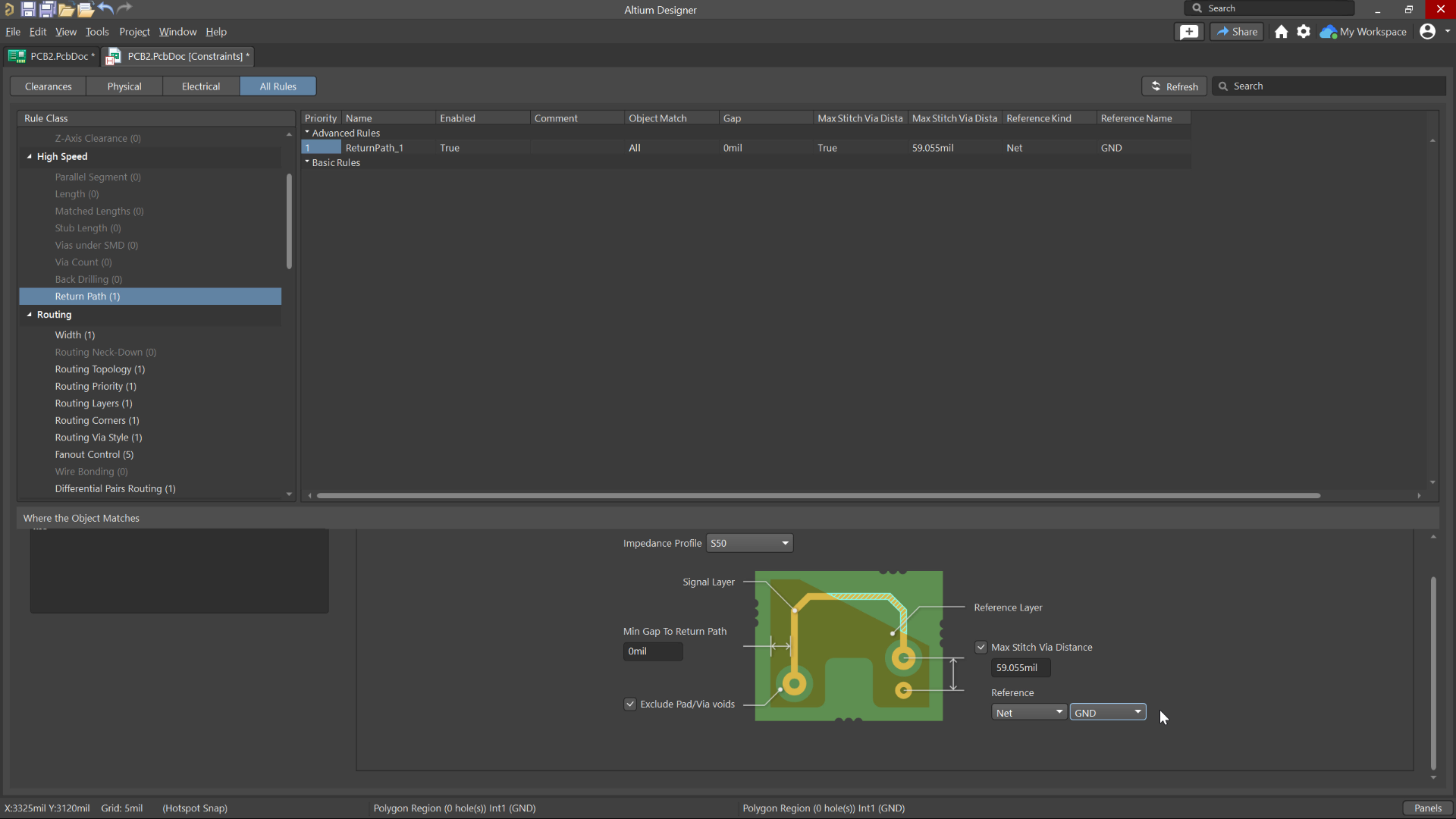
Enhanced Return Path Via Detection
Available in Closed Beta
The enhanced Return Path Via Detection feature improves how stacked and staggered vias are analyzed, enabling accurate validation of return current paths across signal and ground networks in modern HDI PCB designs. It introduces design-aware via recognition and expanded rule reference options that allow you to define exactly which nets or net classes participate in return path evaluation. This delivers more precise DRC results, prevents incorrect stitching assumptions, and helps you identify potential EMI and signal integrity risks earlier in the layout process.
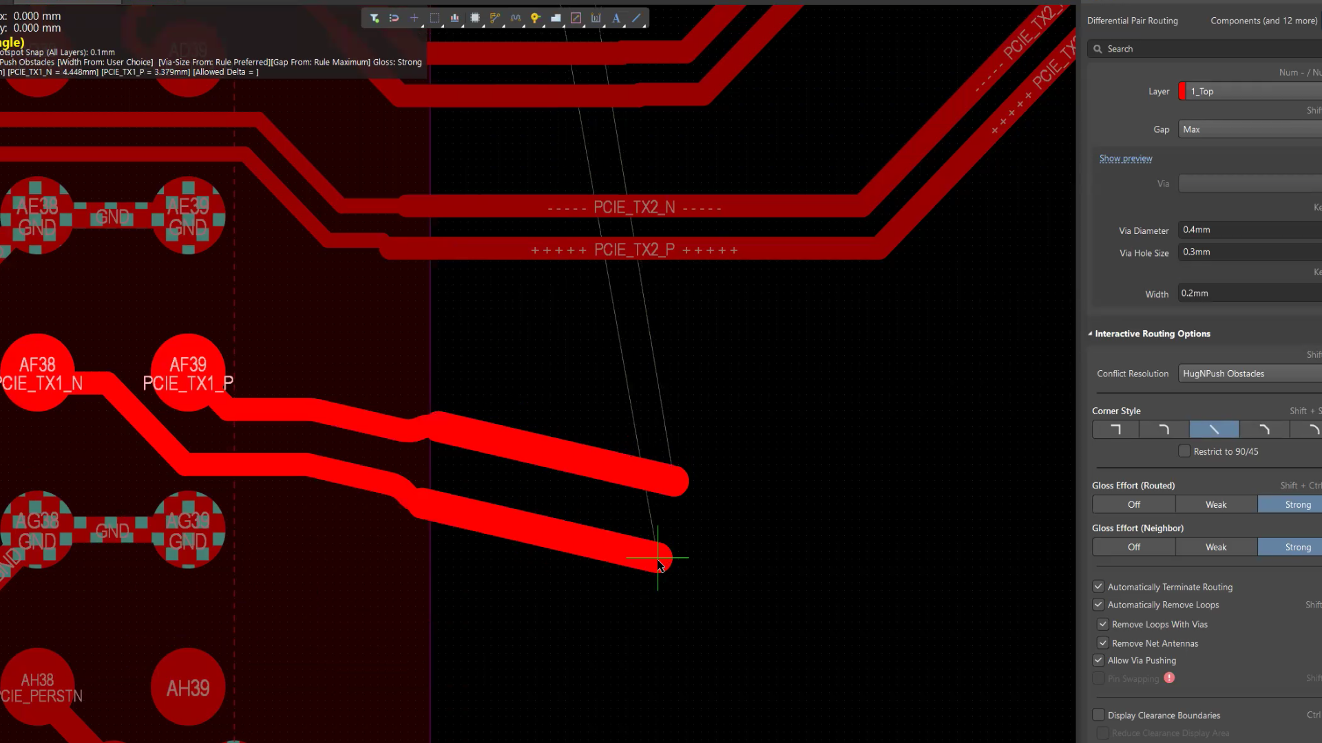
Rounding for Diff Pair Gap/Width Transitions
Available in Closed Beta
The Automatic Rounded Mitering improves any-angle differential pair routing by automatically applying smooth arc transitions at gap and width changes. It introduces intelligent rounded miters during routing, glossing, and retracing to create more natural geometry shifts across boundaries and impedance-controlled regions. This results in cleaner layouts, improved signal behavior, and more visually refined, professional routing outcomes.
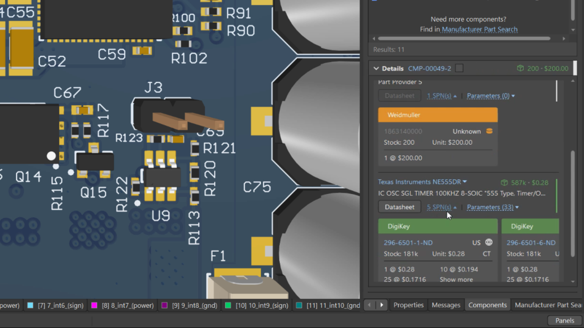
Supplier Data Merging
Available in Open Beta
The Supplier Data Merging feature consolidates supplier information from your custom parts database and the Altium Parts Provider into a single, unified view. It merges and displays this combined supplier data wherever supplier part numbers appear, including in ActiveBOM and during part selection. This provides more complete supply-chain visibility, simplifies sourcing decisions, and reduces the need to reference multiple systems during component selection.
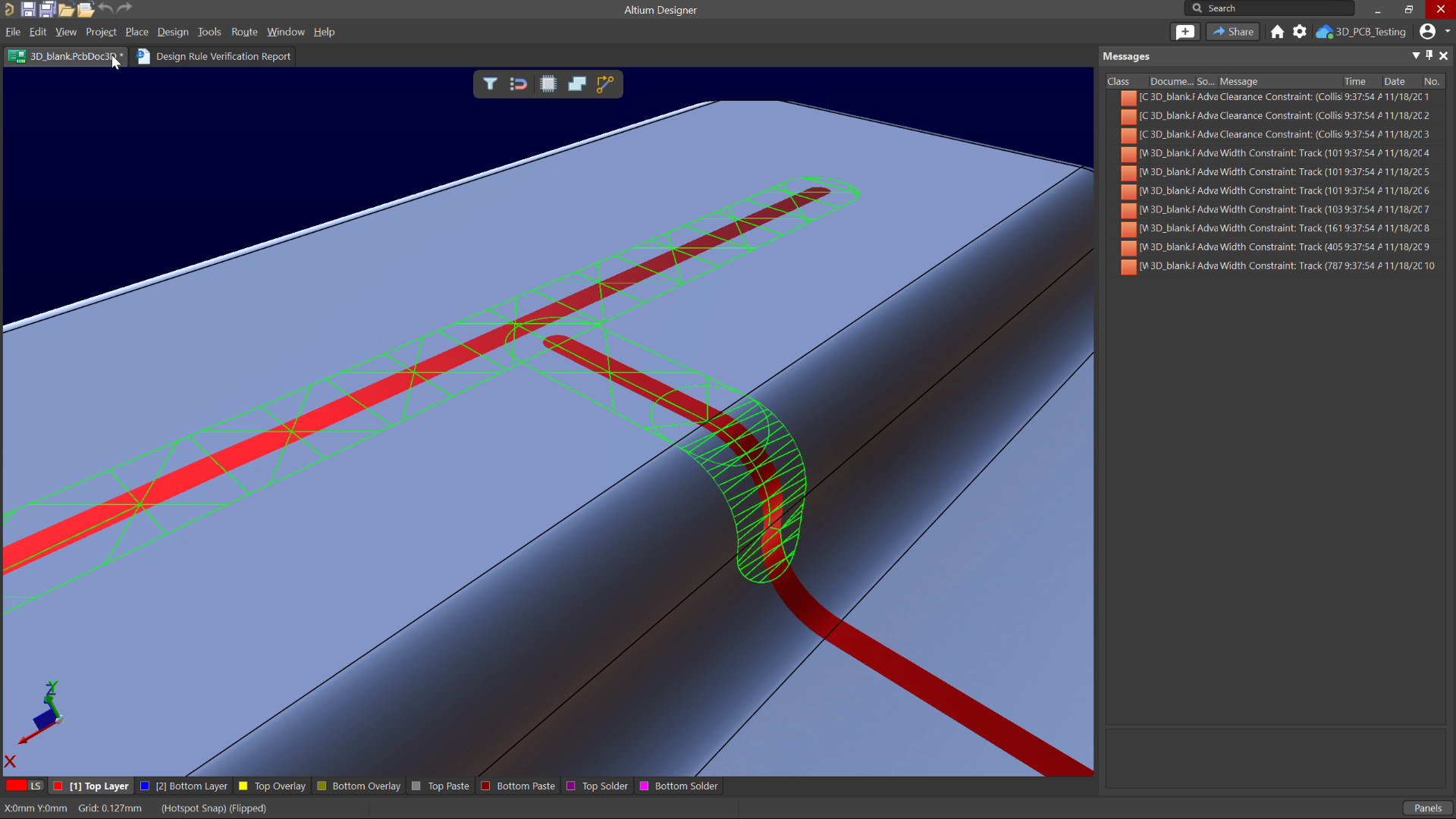
3D-MID DRC
Available in Open Beta
The 3D MID DRC Check feature provides batch design rule checking for routed tracks on 3D substrates, ensuring that Width, Clearance, Length, and Matched Length requirements are all validated against the design. By automatically identifying rule violations across the full 3D geometry, this capability helps to maintain accuracy, prevent manufacturing issues, and confirm that complex 3D routing meets all defined constraints before moving forward.
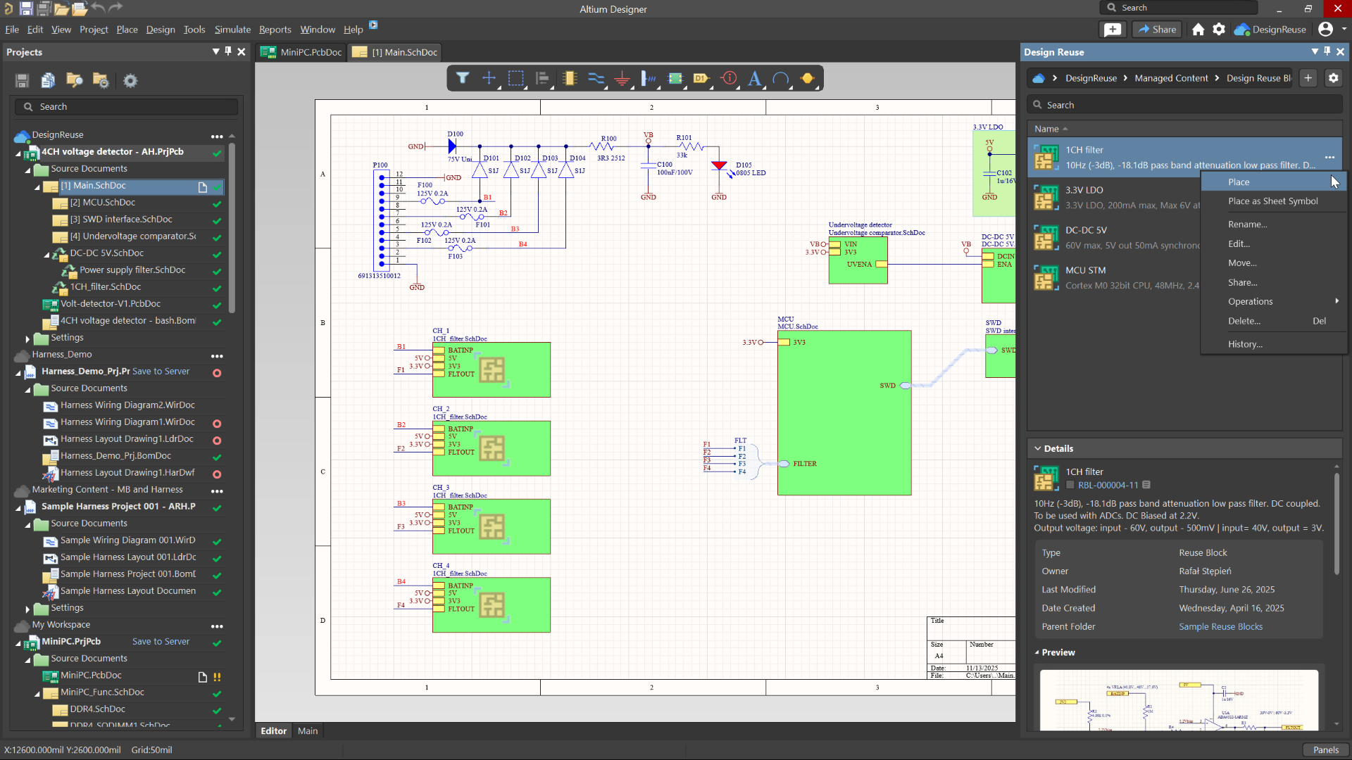
Enhanced Design Reuse Panel
Available in Open Beta
The enhanced Design Reuse panel provides a clearer, more intuitive way to work with reuse blocks and snippets, making it easier to incorporate proven design elements into new projects. The updated panel offers improved organization and navigation, giving faster access to reusable content and helping to maintain consistency, reduce repeated effort, and accelerate development by confidently reusing validated circuitry.
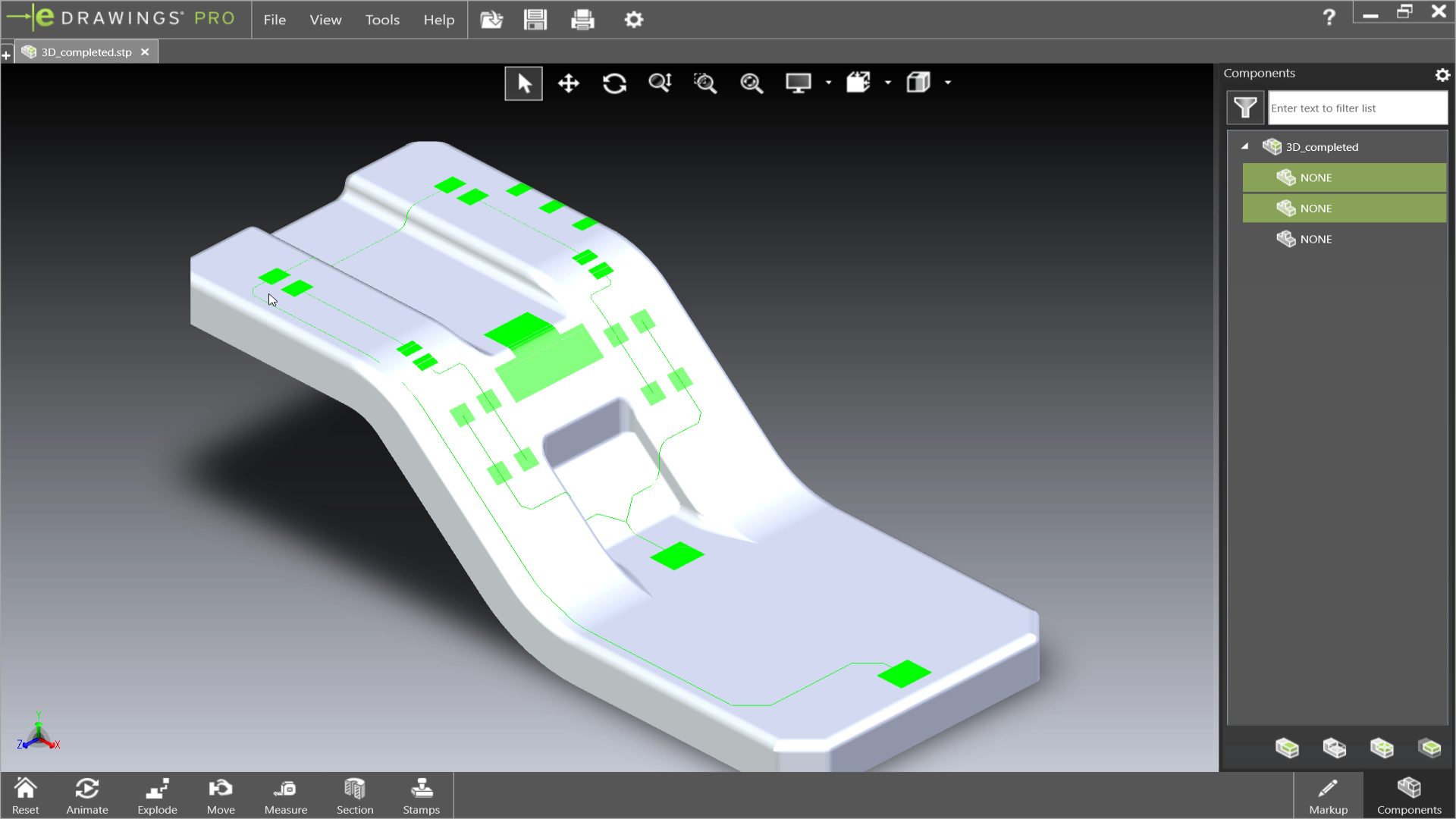
Embedded 3D Models for Harness Designs
Available in Open Beta
Embedded 3D Models for Harness Designs feature automatically embeds Parasolid-format 3D models into harness layout drawings. These models are generated when adding a Physical View for a harness component or connection point, and any existing but unembedded models are incorporated upon saving the layout drawing. This enhances integration with MCAD CoDesigner, facilitating seamless synchronization between electrical and mechanical design domains.
Export 3D-MID Tracks as Centerline Curves
Available in Closed Beta
3D-MID Export of Tracks to Centerline Curves enables the export of conductive tracks on a 3D substrate as precise centerline curves within STEP files, supporting advanced 5-axis manufacturing processes. This achieves more accurate representations of conductive pathways, facilitating seamless integration with mechanical CAD tools and enhancing the precision of manufacturing processes.
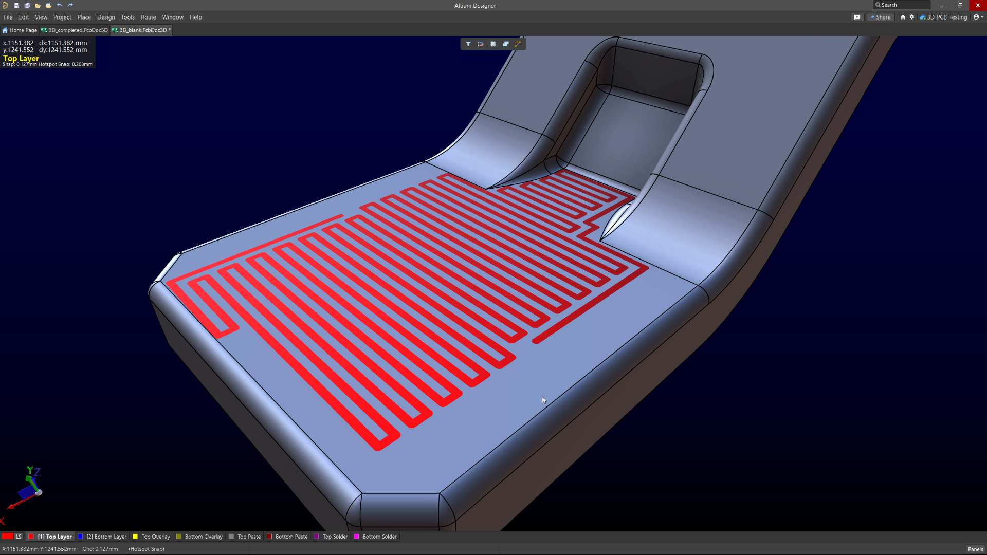
3D Automatic Face Filling
Available in Closed Beta
3D Automatic Face Filling automatically generates a geometric pattern to fill a face of a substrate in 3D-MID designs, based on selected tracks. It creates a patterned covering that extends perpendicular to the track, adapting to surface boundaries and avoiding obstacles. This provides a faster and more efficient way to create protective meshes for security purposes, such as in secure payment terminals, without the need for manual routing.
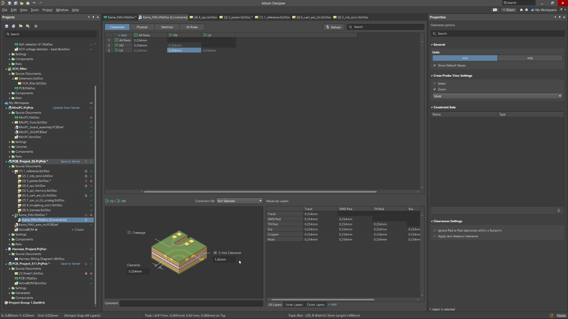
Z-Axis Clearance Rule
Available in Open Beta
The Z-Axis Clearance Rule checks the shortest distance between copper features across different layers in a PCB design. It is available in both the Constraint Manager and the legacy PCB Rules Editor. This rule enables precise layer-to-layer clearance checks for specific net classes, differential pairs, or through schematic parameter directives. It supports both Online and Batch Design Rule Checks (DRC), integrates with polygon pours and PCB CoDesign, and includes optional in-PCB violation overlays for clear visualization of rule breaches.
Advanced Polygon Pour Engine
Available in Closed Beta
Supports true arcs rather than relying on approximated curves during copper pours. This upgraded engine is a substantial improvement to the polygon pour process in Altium Designer. By rendering arcs natively, it delivers smoother and more precise copper shapes, significantly improving visual quality and ensuring cleaner, more professional PCB designs. Additionally, users benefit from faster repour times, streamlining design iterations and boosting overall performance during layout edits.
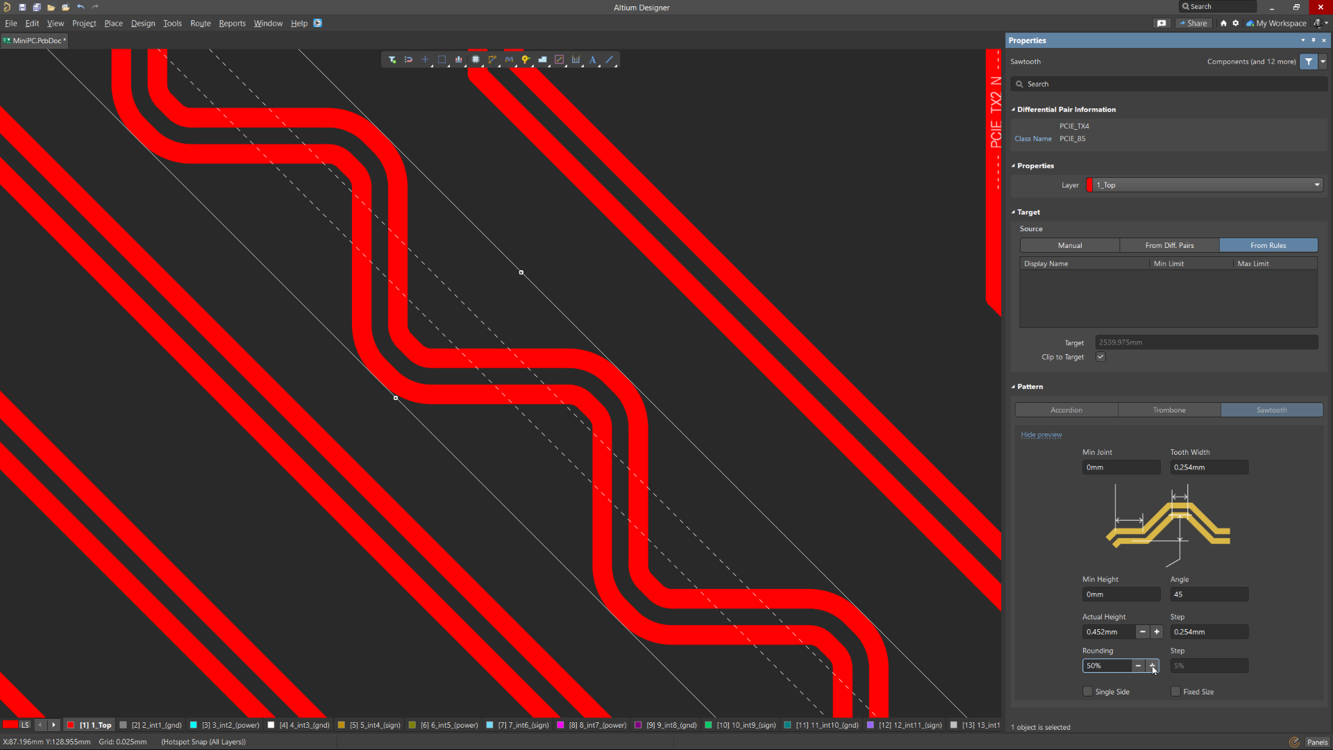
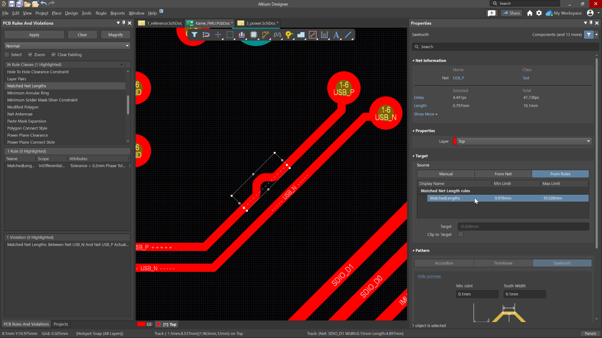
Sawtooth Rounding Support for Length Tuning
Available in Closed Beta
Sawtooth Rounding for Length Tuning enhances the precision of your signal routing by enabling corner rounding on sawtooth patterns during Interactive Length Tuning or within-pair matching in the Auto Tuning process. This feature introduces adjustable rounding levels from 0% to 50% in 5% increments. By smoothing sharp corners in tuned traces, it helps maintain consistent impedance and improve signal integrity—especially critical in high-speed digital designs.
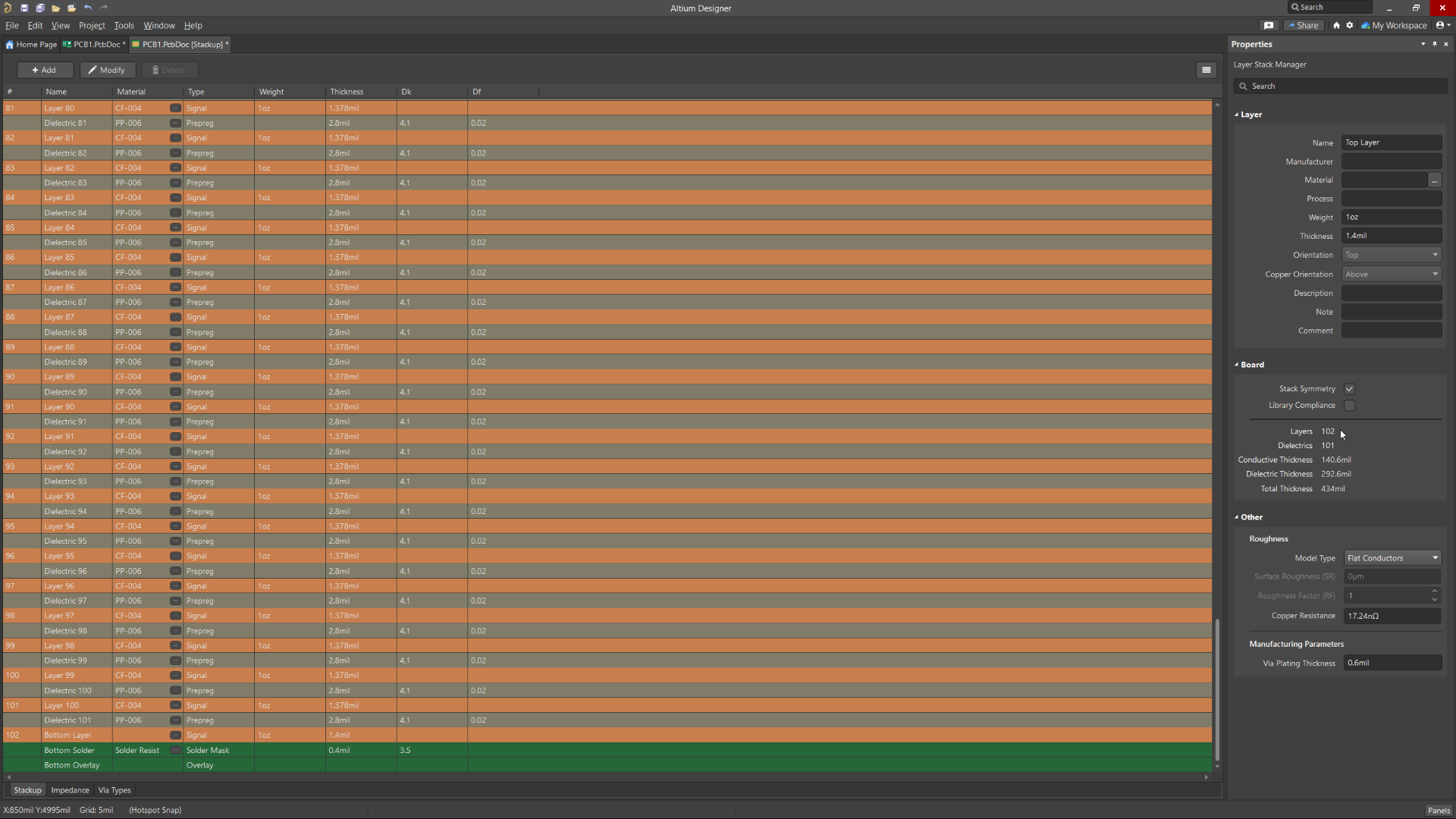
Support for Increased Signal Layers
Available in Open Beta
Increases the number of signal layers available in Altium Designer from the current limit of 32 up to 128. This allows the design of more complex, high-density PCBs, enhancing the ability to handle larger, more sophisticated projects with greater ease and flexibility. Additionally, this enhancement will extend to Allegro and Xpedition importers to enable smooth and accurate importing of PCB designs exceeding 32 signal layers.

Dynamic Re-route on Component Drag
Available in Closed Beta
Dynamic Re-route on Component Drag allows components to dynamically re-route during movement and placement, with configurable limits on the number of connections to optimize performance. This feature streamlines the design process, reduces manual rework, and minimizes errors, leading to faster development cycles and improved overall design quality.

3D Mechatronic Integrated Device Design
Available in Open Beta
The 3D layout tool for Mechatronic Integrated Device (MID) designs seamlessly merges electronic and mechanical elements, opening up possibilities in diverse fields like wearables, medical devices, and automotive components. The tool simplifies the 3D design process with easy integration, synchronized design, logic-driven layout, and precise placement. It also ensures production-ready data export. The tool is user-friendly, eliminating the need for complex workarounds and making it suitable for the entire 3D-MID design process.

Unified Login
Available in Open Beta
Unified Login allows signing in to an Altium Account through an external browser using various methods, including direct email credentials, linked Facebook or Google accounts, or Single Sign-On (SSO). This feature is a streamlined login mechanism integrated with Altium Designer for easy account access.

Static Phase Matching
Available in Open Beta
Static Phase Matching enables the static alignment of differential pair lengths as part of the automatic differential pair length tuning process. This feature is crucial for maintaining the integrity of high-speed signal transmissions across PCB layouts.

Simulation S-parameters Analysis
Available in Open Beta
The Simulation S-parameters (scattering parameters) tool facilitates an approach for describing networks based on the ratio of incident and reflected microwaves. These ratios can be subsequently used to calculate the properties of a circuit including input impedance, frequency response and isolation. While this type of analysis is primarily for RF circuits and components, it is equally useful for any circuit with at least two sources (ports). Using S-parameter data as a tool to optimize your design can lead to cost savings, improved product quality, and a competitive edge in the marketplace.

Simulation Stress Analysis
Available in Open Beta
The Stress Analysis simulation tool computes critical operating conditions like maximum voltages, currents, and power dissipation for components. It examines these conditions against predefined limits specified in a component's stress model, allowing for early identification of potential points of failure. This precision supports the selection of robust components, enhances design efficiency, and minimizes the risk of costly failures, contributing to improved overall design quality and reliability.

Subscribe to the newsletter and
we’ll let you know when the
new version is released.


Be at the forefront of innovative
PCB design technology
Join the Altium Beta Program
Get exclusive access to upcoming features and enhancements while making the tool you use every day even better.
Get Started with Altium Designer
Whether your designs are simple or complex, and you work solo or in a team, Altium has a solution for every engineer or enterprise.
