If the design is large and spread over many sheets, it can become difficult to follow a net and verify the connectivity in the design by simply looking at the schematics. Trying to locate those same objects on the PCB presents an even greater challenge. To help with this process, the Navigator panel is used.

Use the Navigator panel as your view into the entire design. Hold Alt as you click in the panel to also locate that item on the PCB.
The Navigator panel allows you to browse either the active source schematic document or all source schematic documents in the active project. The panel utilizes the connective model of the design, which is automatically created in the background, as its foundation for navigation. The panel can also be used to navigate to components, pads, buses and nets on the PCB.
Navigating the Design
Navigation can be performed in two ways – either by clicking in the Navigator panel to locate that object in the schematic, or by clicking on the object in the schematic to locate that object in the Navigator panel.
The panel retains a history of navigation events for the current editing session, use the buttons at the top of the panel ( ) to move backwards and forwards through the history.
From the Navigator Panel
To display the Navigator panel, use the Panels button at the bottom right of the software, or select View » Panels » Navigator from the menus.
Component and connective Information will load into the panel as soon as a schematic is opened, click on an icon in the Documents section to display it. The software automatically builds a Dynamic Data Model for the entire project, and maintains the model as edit actions are performed. Note that document tabs are not displayed (at the top of the graphical editing space) for all of the schematic sheets (they are opened in the background), a tab only appears when a user-action is performed on that sheet.
The Dynamic Data Model is available for each of the editors, and also the Navigator panel. If at any time you are not sure if the panel contents match the current state of the design, select the Validate Project command to force a refresh of the model (Project menu, or the right-click context menu in the Navigator panel).

Click on an object in the Navigator panel to locate all instances of that object, over the entire design.
Navigation Basics
Navigation Basics
|
| Sections |
The Documents section at the top of the panel gives you different views into the project – individual sheets, the flattened hierarchy (the entire project), and a full design hierarchy. These are discussed in detail later. Click once on an icon in this first section to load the data into the panel, double-click to also display the results in the graphical editing space. |
| Documents section |
In the Documents section, clicking on the entry for an individual document populates the lower sections of the panel with component Instance and Net/Bus information local to that document and where such information exists. Selecting the Flattened Hierarchy entry allows you to peruse all design objects across the entire compiled model of the design. |
| Click to... |
Click once on an Instance / Bus / Net / Pin to locate and highlight that object on all of the schematic sheets that it exists on. |
| Interactive sections |
Note that it is not just the section below that updates when you click on an object. Each section of the panel will jump to the corresponding item in its list when a navigated object related specifically to it. The workspace will also update. |
| What is highlighted |
As you click on an object in the panel, filtering will be applied, the visual result of which is controlled by the Highlight Methods specified on the System - Navigation page of the Preferences dialog (more below). |
| Clear the results |
Press Shift+C to clear the current highlighting across all affected sheets. Note that selection is not cleared using this shortcut, use the X, D shortcut key sequence to clear selections across all sheets. |
| Working in the panel |
Standard Windows grid editing behaviors are available in the panel:
-
Navigate within a section using the Up, Down, Left, Right arrow & Home & End keys
-
Click a column header to sort by that column
-
Click and drag on a column header to change the column order
-
Jump directly to an entry by typing the string, press Esc to clear
|
Interactive Navigation
As well as navigating from the lists of objects presented in the panel and clicking to locate that object in the graphical space, you can also navigate from the graphical space back into the list. Referred to as interactive navigation, you launch this mode by clicking the Interactive Navigation button at the top of the Navigator panel. The cursor changes to a cross-hair, indicating that you are in navigation mode, which it remains in until you right-click or press the Esc key.
As you navigate a design, the sheet display will update in accordance with the current highlighting options and the Navigator panel will update to show information related to your current selection in the graphical editing window.
, then click on an object on the sheet to locate that object in the panel, and across the rest of design.")
Invoke Interactive Navigation (button at the top of the Navigator panel), then click on an object on the sheet to locate that object in the panel, and across the rest of design.
Interactive Navigation Shortcut
As well as launching interactive navigation from the Navigator panel you can invoke navigation at any time in the schematic editor, hold Alt as you click on a design object. You can click on any object, including a wire, net label, port, sheet entry, sheet symbol or component.
Use the Alt+Click shortcut to navigate through your design.
Note that this technique does not support simultaneously navigating the PCB, to do that you will need to use the Interactive Navigation button.
How Objects are Highlighted During Navigation
When you click on an object in the Navigator panel, the object is displayed in the graphical editing space. How the object presents depends on the System - Navigation settings in the Preferences dialog. To access the settings directly from the Navigator panel, click the Navigation Options button ( ) at the top of the panel to open the dialog.
The Highlight Methods region of the Preferences dialog provides options to control the visual result of the temporary filtering that is applied to the document when navigation is performed, from both the panel and within the document itself. Any combination of these options can be enabled. For example, you might want to have all filtered objects zoomed and selected in the design editor window while applying dimming to take away the clutter of other design objects.
Navigation Highlight Methods
Highlight Methods ( ) )
|
| Selecting |
When enabled, the filtered objects will be selected in the workspace. |
| Connective Graph |
Enable this option to display the connective relationship between objects on the active document in the design editor window.
-
The connection lines will be green when navigating by components and red when navigating by nets.
-
When the option is enabled and you are browsing net objects on a schematic, a solid red line indicates a physical connection between net objects, and a dotted red line indicates a logical connection between objects in the net.
-
Enable the Include Power Parts sub-option if you want to also graph the connectivity of power objects.
|
| Zooming |
When enabled, the filtered objects will be zoomed and centered (where possible) in the design editor window. The zoom level (i.e. the extent of zooming applied when navigating from either the panel or interactively within the design document) is controlled using the Far / Close slider bar. A greater zoom level is achieved by moving the slider to the right. |
| Dimming |
When enabled, filtered objects will appear fully visible in the design editor window with all other objects becoming dimmed. Control over the contrast between filtered and masked objects is done using the None / Invisible slider bar. Greater dimming is achieved by moving the slider to the right. |
-
Use the checkboxes in the Objects To Display region to control which objects are included (in the Navigator panel and on the sheet) during browsing.
-
Most of the highlighting options can also be accessed by right-clicking in the Navigator panel to display the context menu ( ).
).
The Navigator Panel
The Navigator panel provides a view into the connective model of the design. The structure of the design is presented in the four sections of the panel, each section is described below.
 The Navigator panel presents a connective-centric view of the entire design.
Documents Section
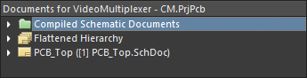
Located at the top of the panel, the Documents section gives you three different ways to view the design – the individual sheets, the flattened hierarchy (the entire project), or the ability to browse through the full design hierarchy. Click once on an icon in this first section to load the data into the panel, double-click to also display the results in the graphical editing space.
Features of the Documents Section
Documents Section
|
Individual Sheets ( ) ) |
Displays an icon for each of the captured schematic sheets, identified by the <Sheet_FileName>. If the project uses repeated sheets (multi-channel design), that sheet will only appear once.
Click once to display the results in the Navigator panel, double-click to also display the results in the graphical editing space.
|
Flattened Hierarchy
(entire project 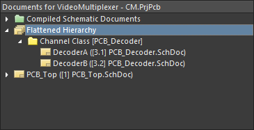 ) ) |
Displays all of the objects and connectivity across the entire project. If there are repeated sheets (channels) in the design, a child icon will display for each channel class, identified by the channel name (derived from the <Sheet_FileName> of the repeated sheet). Within that icon there will be an icon for each channel in that channel class, identified by the <Sheet_Symbol_Designator> ([<AutomaticSheetNumber>] <Sheet_FileName>).
Click once to display the results in the Navigator panel, double-click to also display the results in the graphical editing space.
|
Full Design Hierarchy (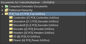 ) ) |
Displays an icon for every logical sheet in the project. If there are repeated sheets (channels) in the design, there is a sheet icon for every channel, identified by the <Sheet_Symbol_Designator> ([<AutomaticSheetNumber>] <Sheet_FileName>).
Click once to display the results in the Navigator panel, double-click to also display the results in the graphical editing space. If you double-click on the icon for a repeated channel, as well as displaying the sheet for that channel, the tab for the specific channel will be selected at the bottom of the schematic editing space.
|
-
The [<AutomaticSheetNumber>] <Sheet_FileName> is displayed as the document tab name at the top of the editing space ( ).
).
-
The channel name, <Sheet_Symbol_Designator>, is the tab name displayed at the bottom of a repeated sheet (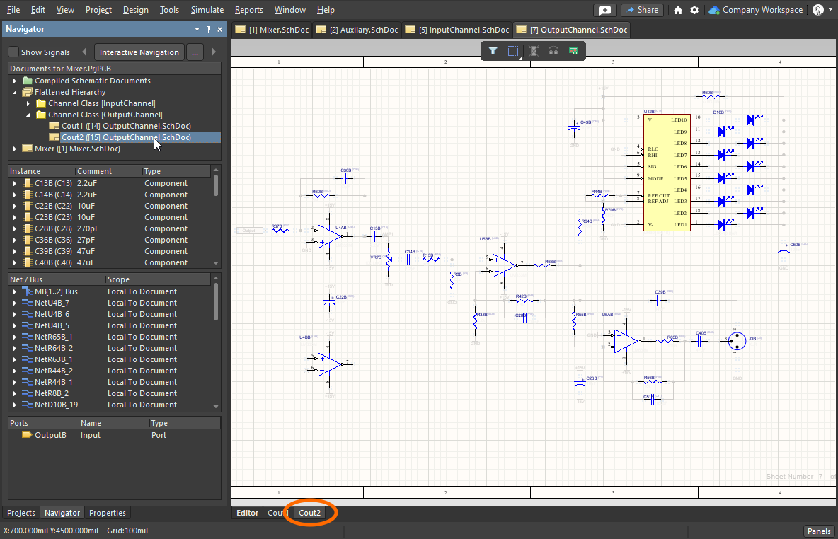 ).
).
Components Section
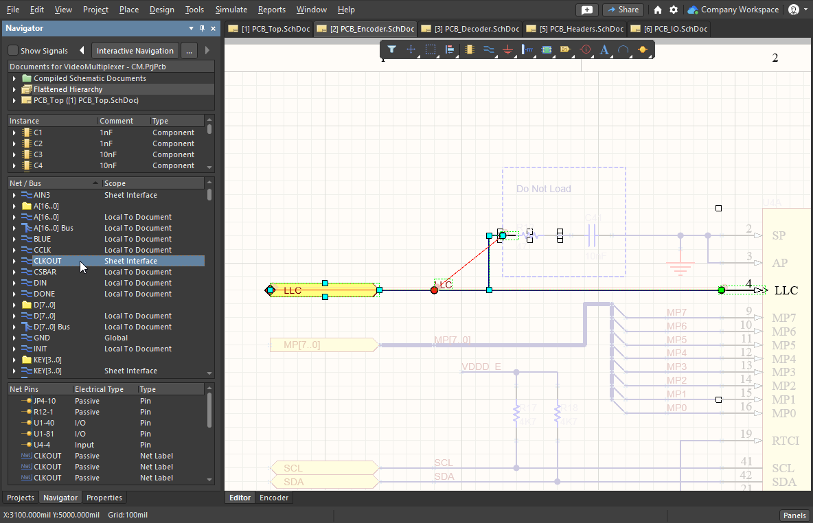
The second region in the panel contains all of the components that exist for the document currently selected in the first section. As you select a top-level component instance entry in the list, a filter will be applied based on that entry, the visual result of which is determined by the highlighting methods chosen. If the enabled Highlighting options includes the Connective Graph option, all other components that are connected to the component you have selected will be visible (the filter having been extended to include them). The connected components are visually highlighted by the green graph connection lines.
 Because the Connective Graph is enabled, a green line is drawn to each component that is connected to the component selected in the panel.
Features of the Components Section
Components Section
|
| Information available |
For each component entry, there are sub-folders for Parameters and Implementations (models). If the Pins option is enabled in the highlighting options, a Pins sub-folder will also be available (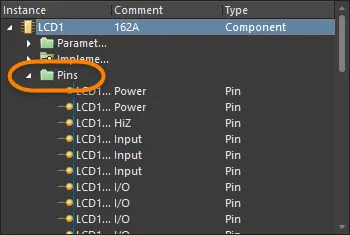 ). ). |
| When you click |
As you click on a pin entry in the Instance list, the corresponding entry for that pin will become selected in the Net / Bus section of the panel and all pins for that parent net will be listed in the bottom section of the panel. A filter also will be applied based on the pin entry you have chosen; the visual result being determined by the enabled highlighting methods. |
| Connective Graph |
If you have enabled the Connective Graph option, all other pins that are connected to the parent net of the pin selected will be visible (the filter having been extended to include them). The parent net for the connected pins is visually highlighted by the use of red graph connection lines (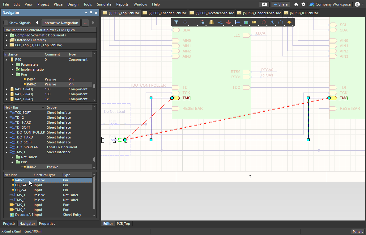 ). ). |
When the Connective Graph option is enabled in the highlighting options, you can also use the Alt+Click shortcut on a component or a pin in the design space to show the graph.
Net / Bus Section
The third section of the panel lists each of the nets and buses in the document (or flattened hierarchy) being browsed. As you click on an entry, all objects associated to the net/bus - Pins, Net Labels, Ports, Sheet Entries and Cross-Sheet Connectors - will be displayed in the design editor window in accordance with the enabled highlighting methods.
Features of the Net / Bus Section
Net / Bus Section
|
| Information available |
The various object types associated with the selected net/bus are listed in sub-folders, depending on the currently enabled highlighting options and the presence of that object-kind in the currently selected net/bus. For each net/bus, a further sub-folder can be included that lists any graphical lines used to connect associated pins/ports/net labels/sheet entries/cross-sheet connectors. Click on a line entry to filter just that line object and apply the visual control settings. |
| When you click |
All net objects that have been enabled for display in the panel (with the exception of graphical lines) will be displayed in the bottom section of the panel ( ). Again, clicking on any of these will apply filtering in accordance with the enabled highlighting methods. ). Again, clicking on any of these will apply filtering in accordance with the enabled highlighting methods. |
Bus Nets - Net Pins Section
The contents of the fourth section of the panel depends upon two things: the object you are navigating, and the objects you have set for display. If you click on a bus in the Net / Bus section, then the nets in that bus are listed in this section of the panel. If you click on a net in the Net / Bus section, then the pins in that net are listed. The net identifiers attached to that net are also listed, if they are enabled for display.

Signal Section
The Navigator panel supports viewing the design in a signal-centric fashion, instead of the object-centric approach that it normally presents the design. If a schematic document is selected in the Documents section of the panel, enabling the Show Signals option at the top of the panel switches the third section of the panel to Signal mode.
Click on a signal entry to apply a filter and the nodes for that signal (pins/ports/net labels/sheet entries/cross-sheet connectors) will be displayed in the design editor window, in accordance with the highlighting methods enabled. For each signal in the list, the node pins, sheet entries or cross-sheet connectors associated with that signal will be listed. These entries will be displayed regardless of whether the corresponding display option for that object type has been enabled or not.

Features of the Signal Section
Signal Section
|
| Signal |
Name of the signal (bus or net name).
|
| Width |
Number of discrete nets within this signal. |
| Click on a top-level signal entry |
Click on a top-level signal entry to populate the bottom section of the panel with all signal nodes associated with that signal. These can include Pins, Net Labels, Ports, Sheet Entries, and Cross-Sheet Connectors. Entries will only be displayed if the corresponding option to display that object type has been enabled. |
| Click on a sub-entry |
Click on a sub-entry in the main Signal list to populate the bottom section of the panel with all net objects associated with the parent net for that signal. |
| SignalName Driven By Pin X |
Displays when a node pin associated with a signal is an output pin or an I/O pin. X represents the component-pin designator that is driving the signal. |
| Driving Node Pin X |
Displays when a node pin associated with a signal is an input pin. X represents the component-pin designator that is being driven by the signal.
|
| Driven By Node Sheet Entry SignalName |
Displays when the electrical type of a sheet entry node is output or I/O, the entry is driving the signal. |
| Driving Node Sheet Entry X |
Displays when the electrical type of the sheet entry is Input, then the entry is being driven by the signal. |
Navigating the PCB
As well as navigating to objects in the schematic as you click in the Navigator panel, you can also navigate to those objects on the PCB at the same time. If you hold the Alt key as you click on an object in the Navigator panel, the target object(s) will highlight in both the schematic and the PCB.
Because navigation always occurs in the schematic, to navigate to objects on the PCB you need to display the schematic and PCB at the same time. You can do this by either displaying the PCB in a separate window, or by sharing the graphical space using the Split Vertical or Split Horizonal feature (vertical shown below). Commands for each of these are available in the context menu when you right-click on a document tab.
Hold the Alt key as you navigate through your design to also locate those objects on the PCB.
Altium Designer includes a number of features for working between the schematic and the PCB, including:
| Cross probe |
Cross probe - Right-click to launch, then click on an object (component, pin, net) in one editor, to jump to that object in the other editor. There are two modes, continuous (remain in the source editor), or jump-to (make the target editor/document the active document), Hold Ctrl as you cross probe to invoke the jump-to mode. Cross probe is supported from: the schematic, PCB and BOM editors; the Constraint Manager; and the Project, Navigator and Messages panels. |
| Cross select |
Click to select a component in one editor, and have it selected in the other editor. Supported between the schematic and PCB editors, enabled in the View menu. |
Learn more about Cross Probing and Cross Selection
Navigator Panel Context Menu

The Navigator panel right-click context menu includes the following commands:


 AI で翻訳