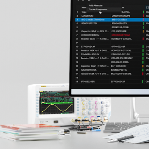
Your workspace is growing. Keep your skills up to date with the latest workflows, best practices & admin tips

Altium Designer Advanced
On-demand Series
Master Complex Boards from Routing to Release
35 Hours of Expert On-Demand Training
Trusted Each Year by Leading Tech & Electronics Companies To Develop Their Teams


Get the Training That's Right for Your Team
Save By Bundling or Choose an Individual Course

The Altium Designer Advanced Series
Master Complex Boards from Routing to Release
3 In-Depth Courses for One Great Price!
Includes All 3 Courses:
- PCB Design Workflows and Best Practices
- Advanced PCB Routing Techniques
- PCB Multi-Channel Design and Templates

PCB Design Workflows and Best Practices
- Master intelligent BOM control, dynamic part selection, and supplier management.
- Implement constraint management in schematic design for seamless PCB transfer.
- Define board shapes from 3D mechanical models and run 3D clearance checks.
- Apply advanced design rule queries, pin swapping, and design variants.
- Build and deploy reusable design blocks to accelerate future projects.
- Enforce creepage compliance for high-voltage and regulated applications.

Advanced PCB Routing Techniques
- Route differential pairs with correct impedance control, length tuning, and accordion/sawtooth patterns.
- Manage complete signal paths across net boundaries with xSignals for DDR, USB, and PCIe.
- Implement advanced via strategies: shielding, stitching, microvias, blind/buried, and via-in-pad.
- Use ActiveRoute and layout replication to accelerate repetitive routing tasks.
- Apply teardrops and back drill configuration for manufacturing-ready HDI designs.

PCB Multi-Channel Design and Templates
- Define multi-stackup rigid-flex boards with correct layer assignments, bending lines, and 3D validation.
- Build multi-board assemblies with synchronized connectivity and mechanical clearance checking.
- Structure repeating schematic channels and replicate placement and routing across rooms.
- Collaborate with multiple engineers on the same board using PCB CoDesign.
- Build reusable Draftsman templates that standardize fabrication documentation across all projects.
- Create project templates that enforce design standards and accelerate every new design start.
Take Your PCB Design Skills to the Professional Level
Now includes the complete advanced workflow, routing, and multi-channel design curriculum in one bundle!
The Altium Designer Advanced Series combines three on-demand courses into one structured learning programme for experienced PCB designers. Together they cover the full arc of professional board development: disciplined workflow and data management, high-speed and high-density routing, and rigid-flex, multi-board, and multi-channel design with company-wide templating. Follow the complete path or target the specific skills your current project demands - each module is a standalone unit you can revisit at any time.
Build Skills That Drive Real Results
• Accelerate complex design cycles with reuse blocks, multi-channel replication, and project templates.
• Route high-speed interfaces with confidence using differential pairs, xSignals, and ActiveRoute.
• Extend your designs into rigid-flex, multi-board assemblies, and collaborative PCB CoDesign workflows.
• Standardize outputs with Draftsman templates and project templates that keep every project audit-ready.
• Practice complex workflows risk-free in interactive simulated environments before applying them to production designs.
• Self-paced access: complete modules in any order, at your own pace, with downloadable reference projects throughout.

Master Complex Boards from Routing to Release
Training Starts at USD 700
Is Altium Designer Advanced Training Right for You?
Whether you're an experienced designer looking to sharpen high-speed routing skills, a senior engineer tackling rigid-flex or multi-board products, or a team lead building reusable design standards - this bundle is built for you.
If you're ready to move beyond the fundamentals and work with the full power of Altium Designer's advanced feature set, the Advanced PCB Design Bundle is your next step.
Need More Training Options?
See All Available Training Courses

Certified Training
Increase your value with a globally recognized certificate from Altium

Job-Ready Skills
Build practical and relevant job skills that companies are looking for

Certified Industry Mentors
Learn from leading industry experts with years of experience to share

Flexible Scheduling
Plan your studies around your work and personal commitments
Requirements:
A stable internet connection
Access to an Altium Account
- Latest Altium Designer installation
This interactive, project-based course ensures attendees gain both the knowledge and practical skills needed to efficiently use Altium Designer and leverage Altium Platform capabilities in their electronic design workflows.
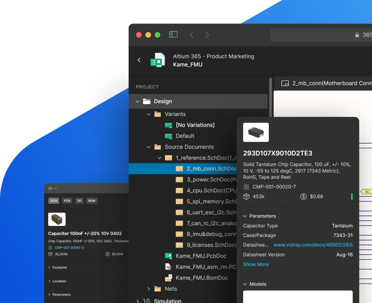
Course Agenda
Series 1: Advanced PCB Routing Techniques
9.5 HoursAdvanced workflow management and industry best practices for experienced designers: intelligent BOM control, constraint-driven design, 3D capabilities, and design reuse strategies.
Key Topics Covered:
- Simulated BOM Environment: Practice real-world BOM scenarios through interactive simulation, mastering part substitution, supplier chain management, and real-time conflict resolution for cost and availability.
- Constraint Manager Integration: Define net classes and rules directly in the schematic environment, propagate them automatically to PCB layout, and validate constraints before any layout work begins.
- 3D Model Import & Validation: Bring in mechanical models, align coordinate systems, extract accurate board outlines, and validate board shape against mechanical requirements prior to layout.
- Advanced Query Syntax: Build sophisticated object-based rule targeting, apply constraints automatically through queries, and reduce manual design rule management with query-driven workflows.
- 3D Constraint Configuration: Set up component-to-component and enclosure clearance rules, identify and resolve 3D clearance violations, and confirm designs meet assembly and manufacturing requirements.
- Pin Swap Configuration: Configure gate and part swapping to improve routing density while maintaining signal integrity, with support for both automated and manual swap strategies.
- Variant Management: Configure population and fitting options across product families, generate independent BOM and assembly outputs per variant, and validate each before release.
- Signal Harness: Simplify multi-signal connectivity in hierarchical designs by creating and configuring harness connectors, and resolving connectivity issues across multi-sheet schematics.
- Design Block Reuse: Capture proven circuitry into versioned, reusable blocks and deploy them consistently across projects with tracked change management.
- Creepage & Compliance: Apply IEC, UL, and other regulatory standards in layout, run automated creepage checks, generate compliance reports, and resolve safety-critical clearance violations.
Series 2: Advanced PCB Routing Techniques
9 HoursSpecialized routing techniques for high-speed and high-density boards: signal integrity strategies, advanced via structures, and manufacturing-aware, automation-assisted layout.
Key Topics Covered:
- Signal Integrity Routing Fundamentals: Covers differential pair routing with impedance control and precision placement, length tuning using accordion and sawtooth patterns, and back drill configuration to eliminate stubs in high-speed stackups.
- xSignals for High-Speed Design: Covers defining and managing complete signal paths across multiple nets and series components, applying matched-length constraints for DDR, USB, PCIe, and similar interfaces, and configuring design rules that govern full signal paths rather than individual nets.
- Advanced Via Techniques: Covers via shielding and stitching for signal isolation and ground plane integrity, implementing HDI via types including microvias, blind, buried, and via-in-pad, and configuring via rules that satisfy both signal integrity and manufacturing requirements.
- Routing Productivity and Design Optimization: Covers ActiveRoute for controlled auto-routing and re-routing workflows, teardrop configuration for improved manufacturing yield and pad reliability, and layout replication to carry proven placement and routing patterns across repeated design blocks.
Series 3: PCB Multi-Channel Design and Templates
16.5 HoursTechniques for rigid-flex and multi-board design, plus designing, managing, and documenting boards built from repeating circuitry and the templates that keep every project consistent and audit-ready.
Key Topics Covered:
- Rigid-Flex 1 - Creating Multiple Layer Stacks: Covers creating multiple stackups within a single board using Layer Stack Manager, assigning materials, coverlays, and impedance parameters to each substack, and validating layer stack definitions before layout begins.
- Rigid-Flex 2 - PCB Design: Covers assigning layer stacks to board regions and defining bending lines, applying correct design rules when routing across rigid-flex boundaries, and verifying the folded assembly in 3D before fabrication release.
- Multi-Board Design: Covers defining board-to-board connections in the multi-board schematic editor, assembling linked boards and verifying mechanical fit in 3D, and synchronizing connectivity updates across all linked projects.
- Multi-Channel Design 1 - Schematic Entry: Covers structuring repeating circuitry using sheet symbols and nested sheets, applying correct designator naming conventions for clean annotation, and confirming channel consistency before moving to PCB layout.
- Multi-Channel Design 2 - Rooms in the PCB: Covers generating and arranging rooms from schematic channels, replicating placement and routing efficiently across all rooms, and applying design rules scoped to individual rooms or the full channel set.
- Multi-Channel Design 3 - Board-Level Annotation: Covers configuring channel-aware annotation to keep designators unique and traceable, back-annotating final designators to the schematic after layout, and documenting annotation clearly for production and assembly handoff.
- PCB CoDesign: Covers configuring a single board for simultaneous multi-engineer work, reserving and releasing design areas to prevent conflicts during parallel editing, and merging contributions from multiple designers with clean conflict resolution.
- Template 1 - Draftsman Templates: Covers building Draftsman templates with standardized title blocks, views, and tables, configuring layer stack and drill drawing views for consistent fabrication output, and exporting templates for reuse across projects.
- Template 2 - Project Templates: Covers building project templates that bundle standard rules, layers, and default documents, managing and deploying consistent starting points across the team, and versioning templates as design standards evolve.
Showcase Your Skills with
Altium Course Certificates
Top Electronics Companies Worldwide Prefer
Working with Altium-Experienced Designers
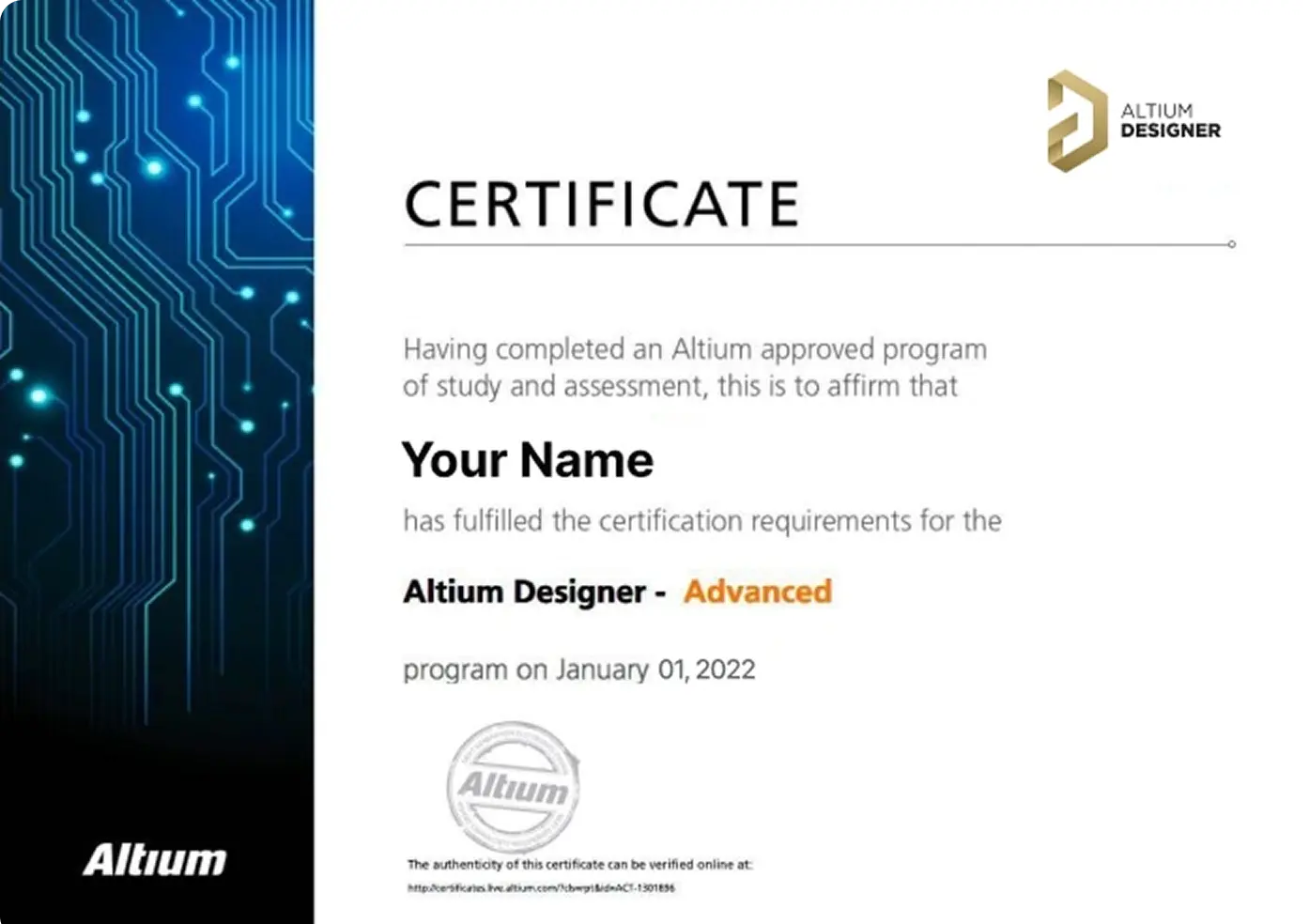
Earn Your Course Certificate
Validate your skills with an official Altium Designer certificate, recognized as a markof expertise in PCB design.
Ready to level up your career? Book your course <br> today and take your skills to new heights.


Skilled PCB Designers Refine Their Craft Through Altium Training
G2 users consistently rate Altium as their top choice for easy-to-use PCB design.
Ready to take the next step in your career? Book your training today!
Altium Training
Loved by Learners, Trusted by Pros
Join a growing community of successful PCB design students.

94% of clients report they are likely or extremely likely to recommend Altium’s Instructor-led training to a friend.

Careers in PCB Design are Growing! According to 2021 survey results published in Printed Circuit Design & Fab (PCD&F) magazine, nearly 78% of the electronic design workforce is projected to retire in the next 15 years
Are you ready to take your career to the next level?
Ready for More?