Chinese - Translation is available for Altium Designer 23:
Go to the pageWith modern digital designs featuring high-speed circuitry, densely populated boards, and multiple low-voltage supply rails, the demands placed on the design's DC Power Delivery Network require an analytical approach to its design. The DC analysis of a Power Delivery Network, or the results of its DC Power Integrity (PI-DC), aims at ensuring that adequate copper has been provided in the path from the voltage sources to the loads – in other words, that the planes, tracks, and vias on the board are of sufficient size (and characteristics) to meet the power consumption requirements of the devices on the board.
Fortunately, the guesswork can be removed from the assessment of a PCB's power delivery network through the use of a DC Power Integrity (PI-DC) simulation tool that analyzes a board design's DC performance based on its electrical and physical properties. Such a tool is available for Altium Designer, the Power Analyzer by Keysight.
Provided as a downloadable Altium Extension, the Power Analyzer integrates directly with Altium Designer to allow PI-DC simulation and analysis of the current PCB project. Since the Power Analyzer functions within Altium Designer, there are no manual data import/export requirements, data conversions, or separate applications to be run – start the Power Analyzer from the schematic or PCB editor, set the desired test parameters, then run the simulation. The results are primarily delivered through 2D/3D modeling of the circuit board copper layout, allowing a quick assessment of the results and the opportunity to perform exploratory 'what if' testing of the PCB layout design.
Accessing the Power Analyzer by Keysight Functionality
To access the Power Analyzer by Keysight functionality in Altium Designer, the Power Analyzer by Keysight software extension must be installed. This extension can be installed or removed manually.
For more information about managing extensions, refer to the Extending Your Installation page (Altium Designer Develop, Altium Designer Agile, Altium Designer).
When you click to download and install the extension, the End-User License Agreement opens (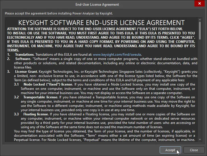 ). Clicking Accept indicates your acceptance of the EULA terms and conditions; when you do, the installation will continue. Clicking Close indicates that you do not accept the EULA terms and conditions, and the installation process will cease.
When the Power Analyzer by Keysight software extension is installed, it gives the ability to:
-
add a new or open an existing Power Analysis document;
-
 configure the Power Analyzer and the power nets;
-
 examine the tree structure of the nets;
-
 examine any existing power analysis results;
-
 view existing reports, and generate new reports from existing power analysis results.
However, in order to perform a new power analysis, you need to be validly subscribed to the Power Analyzer by Keysight. Otherwise, an attempt to start a power analysis will open the Analyze Your Power Nets dialog, where you can request a free trial ( ).
).
Launching the Power Analyzer
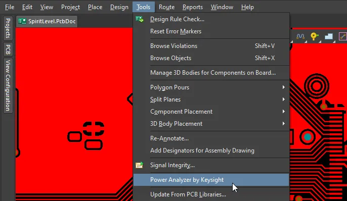
To start working with the Power Analyzer, open the project's PCB document or one of its schematics, and select Tools » Power Analyzer by Keysight from the main menus.
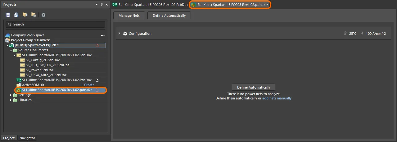
The Power Analyzer Keysight document (<ProjectName>.pdnaK) will open and be added to the Source Documents area for the project (in the Projects panel), as shown below.
Don't have the Power Analyzer by Keysight command available in the menu? Check that the extension is installed and you have a subscription for it (learn more).
The Power Analyzer can be launched from either the schematic editor or the PCB editor menus. However, because the Power Analyzer simulates the PCB structures, any design changes made to the schematic must be synchronized to the PCB before they can be detected from the analyzer document (*.pdnaK). If a design change has not been detected, save, close, and reopen the analyzer document.
Example Project used on this Page
The images on this page have been taken using a modified version of the SpiritLevel-SL1 example board design, the standard version of which is included as part of the Altium Designer installation (\Public Documents\Altium\AD<Solution>\Examples\SpiritLevel-SL1). The following changes to the project have been made:
-
Component
J1, added parameter Component Type, value Source
-
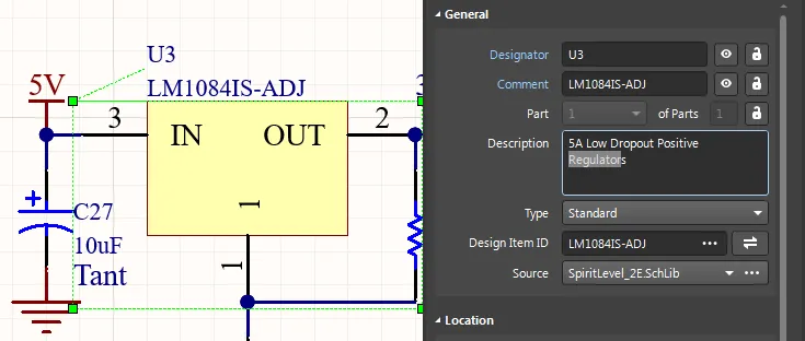
Component
U3, added parameter Component Type, value VRM
-
Component
U4, added parameter Component Type, value VRM
-
Component
LCD1, added parameter Current Consumption, value 0.018
-
Component
LED9, added parameter Current Consumption, value 0.005
-
Component
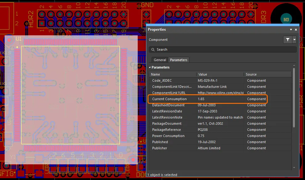
U1, added parameter Current Consumption, value 1.65, added parameter Power Consumption, value 0.75
-
Component
U2, added parameter Current Consumption, value 0.005
-
Component
U5, added parameter Current Consumption, value 0.1, added parameter Power Consumption, value 0.1
-
Component
U6, added parameter Current Consumption, value 0.005
-
Component
Y1, added parameter Current Consumption, value 0.012
-
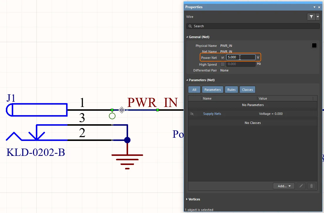
SL_Power.SchDoc, PWR_IN net, set Power Net property to value 5V (refer to this section for details on how to enable this property)
-
The net
1V8 was also named VCCINT (the net had multiple names), and the net 3V3 was also named VCCO. References to VCCINT and VCCO were removed to simplify the design, leaving the nets named as 1V8 and 3V3.
This modified example project also includes a pre-made Power Analyzer by Keysight document (SL1 Xilinx Spartan-IIE PQ208 Rev1.02.pdnaK), shown below, which you can use to run a power analysis for this design to see the feature in action.
Preparing for Analysis
Ready to perform an analysis, but when you click the Analyze button a dialog opens offering access to a Trial? Check that the extension is installed and you have a subscription for it (learn more).
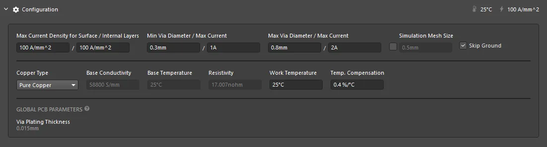
The Power Analyzer needs to know the physical properties of your board. These include maximum current densities for the surface/internal layers, minimum and maximum via diameters, the type of copper, the working temperature and so on. These properties are defined in the Configuration region of the analyzer document.
Configuration Options
-
The maximum current density and maximum via current values are the same for all nets because they depend on the copper geometry.
-
The Max Current Density for Surface / Internal Layers settings specify the allowable value for the corresponding layers of the PCB.
-
The maximum current in vias is specified for the minimum and maximum hole sizes used in the project. Hole diameter values are defined in the Min Via Diameter and Max Via Diameter fields, along with the Max Current allowed for that hole size.
-
The software divides the PCB layout into meshes during the simulation process. By default, dynamic mesh size is used. By enabling the Simulation Mesh Size checkbox, you can define the required mesh size.
-
The default setting is to exclude the Ground net from the Heatmap results. To include the Ground net, disable the Skip Ground checkbox, then select the GND net in the Network / Net dropdown at the top of the Power Analysis by Keysight panel to explore the Heatmap results. Note that the Heatmap supports polygon structures on signal layers, but the behavior of a power plane layer cannot be simulated.
-
The Copper Type field specifies the type of copper used, along with its associated parameters and the temperature parameters.
-
The Work Temperature is used to determine the resistivity of the conductors, and the Temperature Compensation is a criterion of the material itself related to its thermal conductivity. Different materials have different thermal conductivity coefficients and, accordingly, will affect the heating of the material depending on the load. This heating will affect the internal resistance of the material, which in turn will affect the Voltage Drop.
-
The Via Plating Thickness displayed in the Global PCB Parameters region is defined Properties panel of the Layer Stack Manager – learn more.
Change these from the defaults as needed to suit your design.
As well as the max current density and max via current, the allowable voltage drop value must be specified for each power net that is defined. Configure the DC Drop Limit for each net, either selecting a predefined percentage or entering a Custom value.

The Auto-Define Settings are used by the Power Analyzer when attempting to define the power nets from your design automatically. To do this, it needs to know how to identify circuit elements such as voltage regulators, connectors, and series components. As well as using clues such as component designator prefixes, you can also add parameters to certain components to enhance the automatic detection process. For more information, refer to the Auto-recognition Requirements section.
Adding a Power Net for Simulation
To add a power net for simulation, click the button in the upper left to open the Manage Nets dialog. Enable the check box for the required Power Net Name and configure the corresponding Reference Net. If a net has no power port object in the schematic design, it will not be presented in the Power Net Name list. Click Show Custom Nets to include all nets in the design. Multiple power nets can be enabled if required. Hierarchical relationships between power nets are resolved automatically once the power net is fully configured.
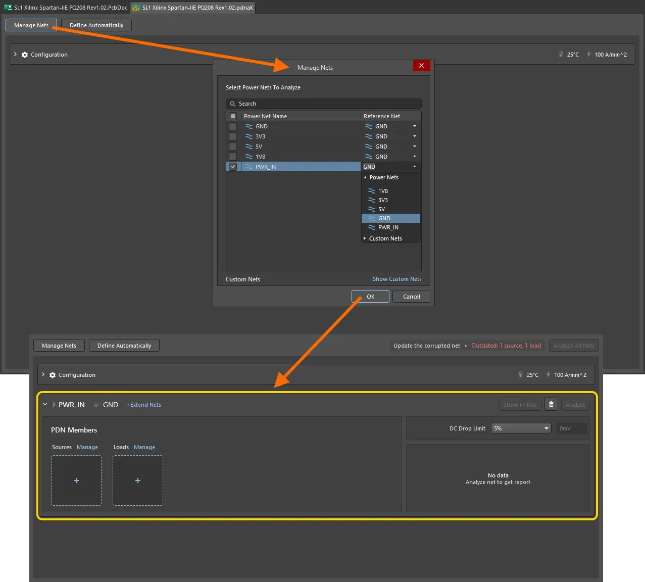
Each power net requires a power source, these will be configured next.
You can also click the
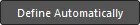
button to have the software create the power nets for you, which it attempts to do by automatically recognizing the topology of the project, based on the current settings in the
Auto-Define Settings region of the
Configuration section in the analyzer document (
*.pdnaK).
Adding a Power Source
To add a power source, click the + (or the associated Manage control) in the Sources section of the desired power circuit. If the circuit includes more than one power source, click Manage and select the remaining components.
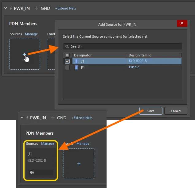
For a component to be available as a source, it must connect to the selected Power Net, but can connect to the selected Reference Net through any component that is connected to that Reference Net.
The Component Card
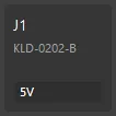
Each component that is included as a Source or Load is represented in the Power Analyzer document by a Component Card.
-
Hover
![]() over the Component Card to display the Edit and Delete buttons.
over the Component Card to display the Edit and Delete buttons.
-
Double-click on the Component Card to open the Properties dialog for that component.
-
Click on the Design Item Id
![]() value to cross-probe to that component on the schematic. The cross-probe zoom level is defined in the Highlight Methods section of the System - Navigation page of the Preferences dialog.
value to cross-probe to that component on the schematic. The cross-probe zoom level is defined in the Highlight Methods section of the System - Navigation page of the Preferences dialog.
-
Edit that component's main analysis value
![]() directly in the Card (or Edit the component to access all of the properties).
directly in the Card (or Edit the component to access all of the properties).
Extending a Net
Power nets on the board can pass through passive elements, such as fuses or resistors, which will have a different net on the other side of that component. In this situation, it is recommended to extend the net by including an intermediate component and its second net as part of the main net. The Extend Nets function is used for this purpose.
To extend a net, click on the +Extend Nets icon next to its name to open the <PowerNet> Extensions Manager dialog. Click the + to extend the target net. The Power Analyzer only displays nets that can be connected through a single extension component. Once you Add the net, a related component will be added automatically in the <PowerNet> Extensions Manager dialog, which can be changed if desired.
 Power nets can be extended through a series component.
You can then continue to extend the net by clicking the + symbol, as shown in the image below. When complete, click Save in the <PowerNet> Extensions Manager dialog.
 Continue to add series components and nets.
Notes on Extending a Net
-
For each series component, you can set its voltage drop, resistance, and maximum allowable current, which will be taken into account during analysis (show image![]() ).
).
-
If you define an incorrect net, you can delete it by hovering over its name and clicking the delete icon that appears.
-
Once the extended net has been saved, the components connected to the extended nets will appear in the list with loads, and you will be able to add them.
-
Next to the power net name, you can see the number of extensions that have been added, hover the cursor over the number to display the names of the extension nets (as shown in the image above).
-
Simulation support for parallel components in an extended net was added in PABK extension V1.0.6, and user-interface support was added in PABK extension V1.0.9. To define parallel components, select the net in the Extensions Manager dialog pop-up, then enable all of the parallel components, as shown in the image below. Hover over the image to show the dialog once net extending has been completed.
 Select all of the parallel components in the net.
Specifying a Load
To add a load component, click the + (or the associated Manage control) in the Loads section and then select the desired component. A component is listed in the dialog when it is connected to the main or an extended net.
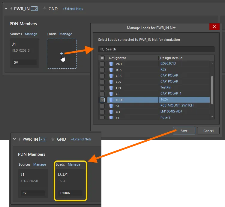
After adding a component, you can specify its consumption either directly in its Component Card, or by clicking the  button to open the <NetName>/<LoadName> Load Properties dialog.
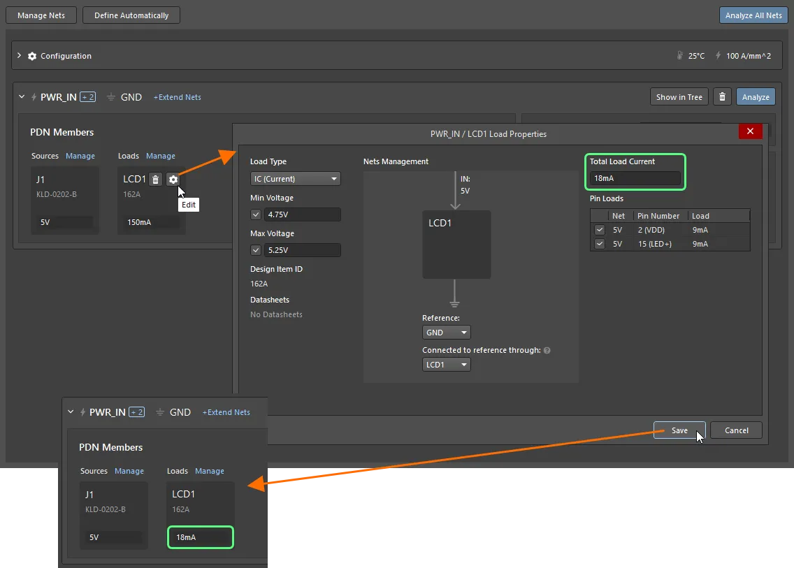
Notes on Configuring a Load
-
Define the load properties, including the Load Type, Total Load Current, and Min and Max Voltage.
-
Confirm that the supply net IN is configured correctly, as well as the Reference and Connected to reference through options.
-
The Load Current is automatically shared equally between all identified power pins; modify these values if required.
-
When configuring a load of the IC (Current) type, you can see all pins of the load component that connect it with the source through different serial components, with the ability to select the required pins.
When the Manage Loads (or Add Sources) dialog is open, it includes a Design Item Id column. Click on an entry in this column to cross-probe to that component on the schematic, making it easier to verify that you are selecting the correct component.
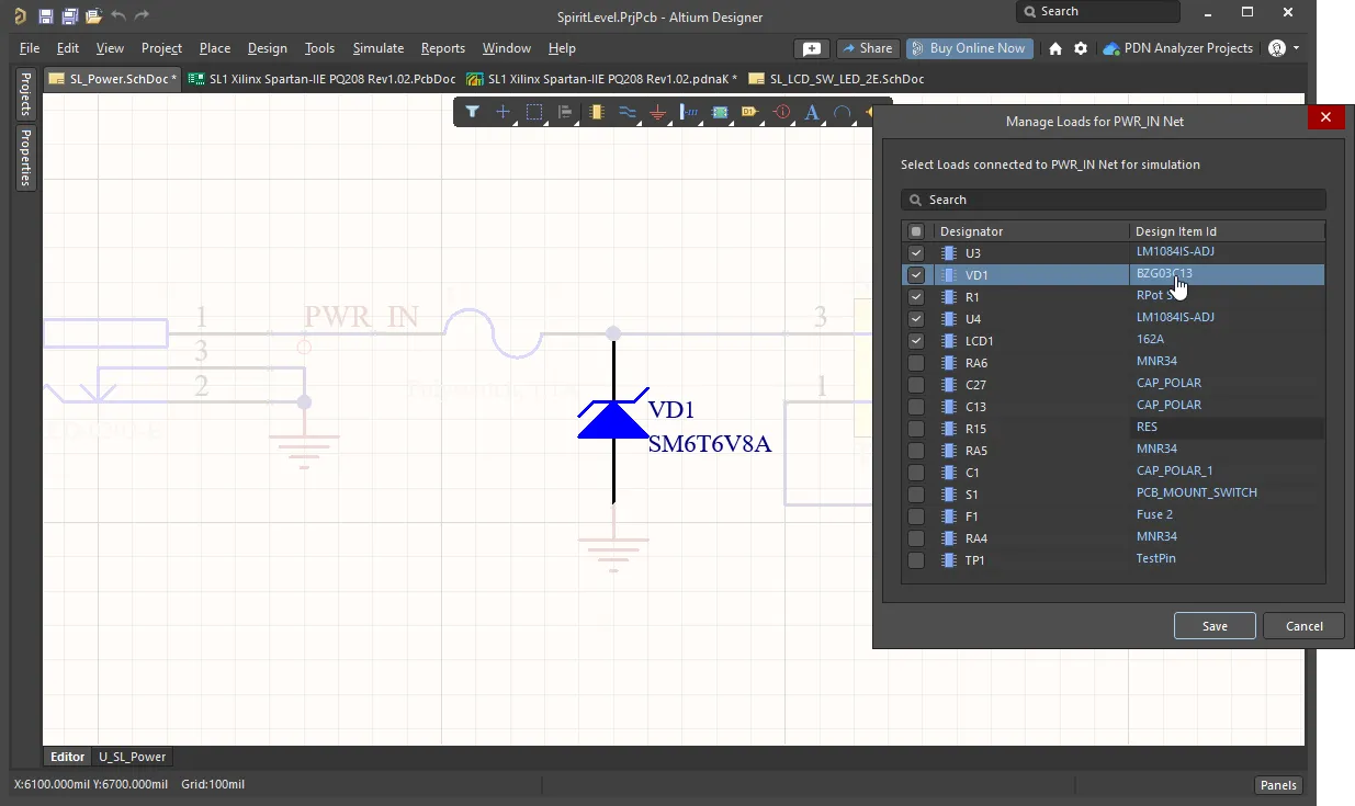
The cross-probe zoom level is defined in the Highlight Methods section of the System - Navigation page of the Preferences dialog.
Specifying a VRM
To define a Voltage Regulator Module (VRM) component, first, add it as a load. Then open the component Load Properties dialog (click the  button), to configure it.
 Once a load has been configured as a VRM, it will also appear as the source for the power net specified as its OUT net.
Notes on Configuring a VRM
-
Specify Load Type as the VRM of the desired type.
-
Specify the output voltage in the Vout field, along with the other regulator properties.
-
Configure the IN and OUT nets in the Nets Management region of the dialog.
-
If the VRM does not connect directly to the reference net or uses a different reference, configure the Reference and Connected to reference through options as required.
-
A child power network is automatically created in the hierarchy with that VRM as the source (as shown above).
-
If the VRM has more than one output net, add all necessary nets using the +Add Out Net link in the Load Properties dialog, and specify their output current in the corresponding fields that appear.
The Configured Power Net
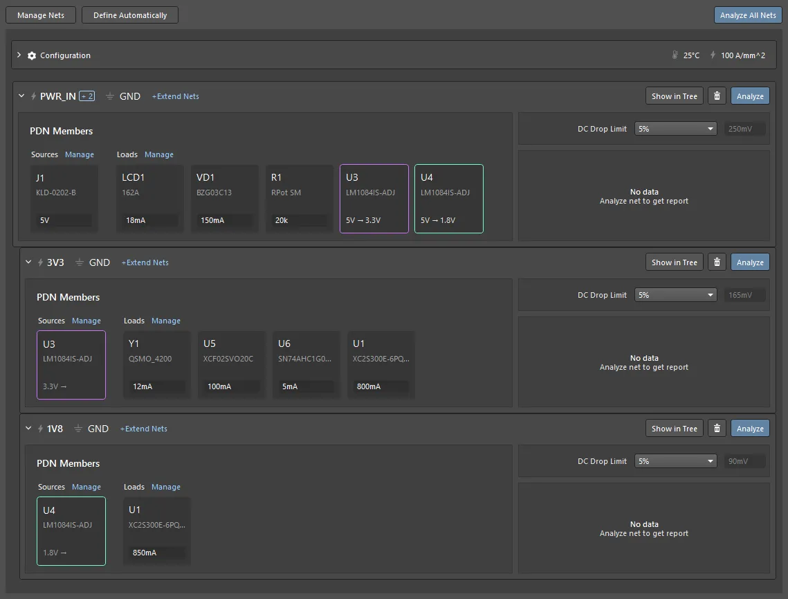
Each configured power net presents as a separate collapsible definition in the *.pdnaK document, the configured PWR_IN net is shown below, with its two child power nets, 3V3 and 1V8, indented slightly to indicate their child-net status.
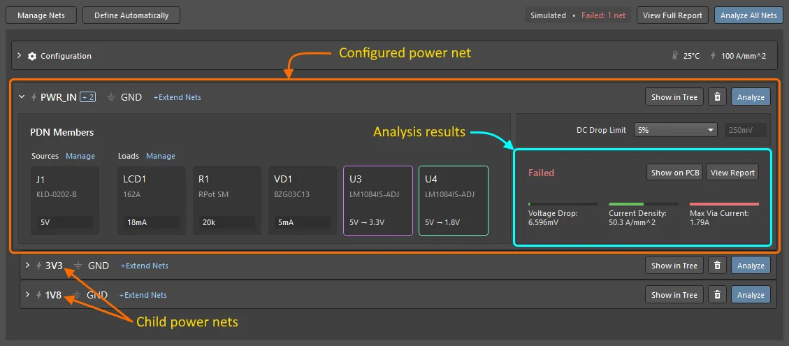
Understanding the Power Net Definition
-
Each power net presents as a separate collapsible Power Net Definition.
-
The banner of Power Net Definition includes:
-
The power net name

-
The reference net

-
An indicator showing the number of additional nets (
 ), if the net has been extended. Hover to show the names of the child net(s).
-
A button, click to show the connective structure of the components in this net, within the context of the entire power net hierarchy.
-
A
 button, click to delete this net from the analysis process, along with all child nets.
-
An
 button, click to analyze this net, along with any child nets.
-
Each component in the net is represented by a Component Card.
-
Once the net has been analyzed, the Voltage Drop, Current Density and Max Via Current results for that net are shown in the Power Net Definition, as shown in the image above.
-
Each gauge shows the simulated value relative to its specified limit. If the value is completely within the limit, the scale line is green. If it is close to the limit the line is yellow, and if the limit is exceeded, the line is red.
-
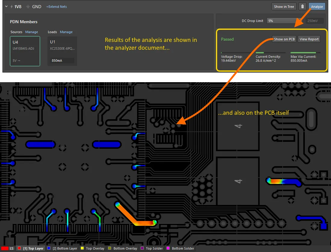
Click the button to switch the view to the PCB editor, showing the copper within this net on the PCB. In the PCB editor, use the Power Analyzer by Keysight panel to control the analysis process.
-
Click the button to generate and open a detailed report about that power net. Within the report, use the
 button to save an HTML copy.
The Tree View of Power Nets
Switch to viewing the configured power net (and any child-nets defined through VRMs) in a tree-like fashion by clicking the associated button. The whole structure will be shown, with the specific power net and associated components highlighted accordingly.
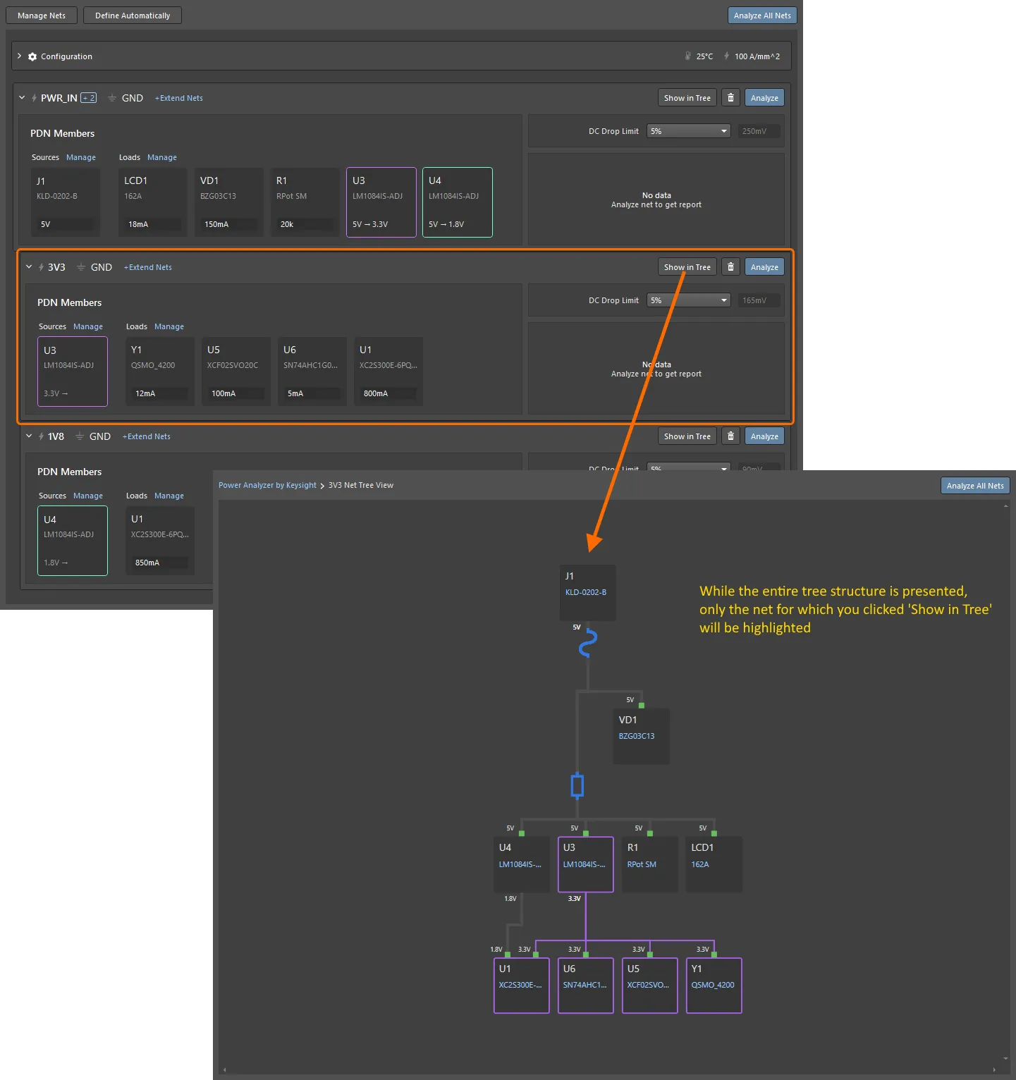
The Tree view lets you quickly assess whether the full power network has been defined as required and is ready to analyze. To return to the main window, click the Power Analyzer by Keysight link in the upper left corner of the .pdnaK document.
Running an Analysis
With the configuration complete, you can proceed to run an analysis for a specific net by clicking its associated button. A summary of the analysis results are presented in the Power Net Definition, as shown below. To see the results within the PCB, click the associated button.
To analyze all of the configured nets in a single action, click the

button (at the top-right of the analyzer document). If you choose to analyze the top-level power net in the tree structure, then all sub-nets (created through VRM components) will also be analyzed. If all nets have been analyzed, you can select which net is currently highlighted using the
Network/Net dropdown at the top of the
Power Analyzer by Keysight panel.
Layer Management
Switching layers of the simulation can be done in the same way as when working with PCB - via the layer tabs at the bottom of the PCB Editor window. You can also focus on the current layer with the Shift+S shortcut, use this shortcut to cycle through the Single Layer Mode visibility options.
 Use the PCB layer tabs to quickly switch the display of analysis results. Shown here are the results for the Top Layer. Hover over the image to see those for the Bottom Layer.
The Power Analyzer by Keysight Panel
In the PCB editor, the analysis process and results are controlled through the Power Analyzer by Keysight Panel. Note that the panel is added to the list of available panels (via the Panels button) after a power analysis has been performed and the button has been clicked.
Network / Net
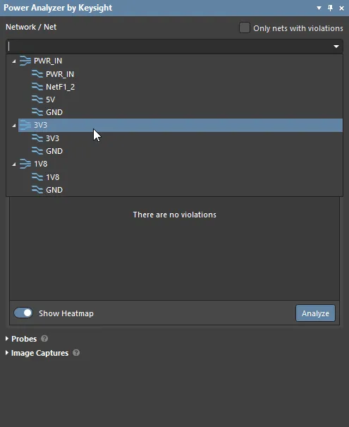
-
Network / Net - used to select the Network (
 ) or Net (
 ) you want to be displayed as a heatmap in the graphical workspace.
-
Only nets with violations - when this option is on (the default), only nets that currently have a violation are available in the dropdown. Clear this option to list all power nets.
-
Use the standard PCB editor techniques to pan and zoom around the workspace to examine the simulation results.
Below the Network / Net selector, the panel has two tabs, General and Heatmap. The options in these tabs apply to the Net currently selected in the Network / Net dropdown.
 Select the net to display, then configure the General or Heatmap options for that net.
Heatmap
The Heatmap Tab on the Power Analyzer by Keysight panel is used to control what data is presented as a heatmap, either the Current Density or the Voltage Drop, and how color is applied to the current density or voltage drop.
 Use the Heatmap tab of the Power Analyzer by Keysight panel to change simulation results presented on the PCB. Here, the Current Density results are displayed. Hover the cursor over the image to see the Voltage Drop results.
The options for each of these modes are described below.
Heatmap for Current Density
-
The entire net is colored to reflect the Current Density at every location along the net, where the higher the current density, the hotter (redder) the color.
-
Show Heatmap - use this control to quickly remove the heatmap and restore the standard display of the PCB.
-
Show Arrows of Current Direction - enable this option to display small arrows indicating the direction of current flow throughout the net.
-
Use Noise Suppression - As the calculated current approaches zero, current direction arrows give the impression that there is current flowing in that area, where there is essentially none. Enable this option to exclude these lighter-current, potentially-misleading values.
-
Scope Controller - how color is applied to the net to display intensity, or heat, is controlled by the Scope Controller. The Max value defaults to the maximum calculated current density in that net (show image
![]() ), and the Min defaults to 0 A/mm2. This scale is displayed as a colored bar below the PCB, reflecting: the current Min and Max settings, a scale determined by the selected Scale type, and the units. The Min and Max values can be adjusted by clicking and dragging on the slider, or by entering a new value in the Min or Max fields. Calculated values below Min are displayed in blue, and values above Max are displayed in red.
), and the Min defaults to 0 A/mm2. This scale is displayed as a colored bar below the PCB, reflecting: the current Min and Max settings, a scale determined by the selected Scale type, and the units. The Min and Max values can be adjusted by clicking and dragging on the slider, or by entering a new value in the Min or Max fields. Calculated values below Min are displayed in blue, and values above Max are displayed in red.
-
Use Logarithmic Scale - enable this option to switch the scale from linear to logarithmic. A logarithmic scale has the effect of concentrating higher values towards the hot end of the color scale. For example, you might enable the Logarithmic scale to quickly locate sections of routing carrying higher currents, then switch to the Linear scale to examine the spread of current densities within that section of routing.
 Logarithmic current density heatmap shows an area of concern, hover your cursor over the image to show that area displayed using the linear scale.
Heatmap for Voltage Drop
-
The entire net is colored to reflect the Voltage Drop at every location along the net, where the higher the voltage, the hotter (redder) the color. Using this approach, the colder the color, the lower the voltage (and the greater the voltage drop).
-
Show Heatmap - use this control to quickly remove the heatmap and restore the standard display of the PCB.
-
Show Arrows of Current Direction - enable to display small arrows indicating the direction of current flow throughout the net.
-
Use Noise Suppression - As the calculated current approaches zero, current direction arrows give the impression that there is current flowing in that area, where there is essentially none. Enable this option to exclude these lighter-current, potentially-misleading values.
-
Scope Controller - how color is applied to the net to display intensity, or heat, is controlled by the Scope Controller. The Max value defaults to just below the specified maximum voltage for that net, and the Min value is
Max - calculated voltage drop (show image![]() ). This scale is displayed as a colored bar below the PCB, reflecting: either the voltage drop as an absolute value or a percentage, the current Min and Max settings, and the units. The Min and Max values can be adjusted by clicking and dragging on the slider handles, or by entering a new value in the Min or Max fields. Calculated values below Min are displayed in blue, and values above Max are displayed in red.
). This scale is displayed as a colored bar below the PCB, reflecting: either the voltage drop as an absolute value or a percentage, the current Min and Max settings, and the units. The Min and Max values can be adjusted by clicking and dragging on the slider handles, or by entering a new value in the Min or Max fields. Calculated values below Min are displayed in blue, and values above Max are displayed in red.
-
Scale Type - the voltage drop scale can either be expressed in volts (click the
 button), or as a percentage (click the
  button).
-
Enable Visual Slider for Voltage Contour - when enabled, displays the location(s) on the heatmap where the voltage is equal to the specified Voltage Contour Points, allowing you to readily identify those locations. Contour Point values can be adjusted by dragging the sliders, or by typing values in the Voltage Contour Points fields below. Additional points can be added and existing points removed by clicking the corresponding icon.
 Contour Points can be configured to quickly identify the locations on the board where the voltage is at that value.
Violation Detection
If the simulation detects a: Voltage Drop, Current Density or Max Via Current violation, they are listed in the Violations section of the Power Analyzer by Keysight panel. Click on a violation in the panel to cross-probe to the specific location on the PCB where that error occurred. If you cannot read all of the violation description, hover the cursor over the Description section of the violation to display a tooltip showing all of the details.
 Violations are automatically detailed in the Violations section of the Power Analyzer by Keysight panel. Hover the cursor over the image to show a Via Current violation.
Note that the heatmap mode (Current Density or Voltage Drop) is automatically selected, based on the type of violation that you click on.
Probes
The Probes section of the Power Analyzer by Keysight Panel is used to place measurement probes directly on the PCB. Probes can either measure Current Density or Voltage Drop, the type of measurement is determined by the current heatmap mode of the board.
Probes can either be:
-
A Single Probe, to measure an absolute value at the probe site, or
-
A Difference Probe, to measure the difference between the two probe sites.
Both types of Probes are placed by clicking the  button in the Probes region of the panel. To place a Single Probe, click at the required location then right-mouse click (or press Esc). To place a Difference Probe, click once to define the first probe site, then click a second time to define the second probe site. Once a Probe has been defined, the measurement results will be displayed in the panel.
When placing a probe, the same snapping features apply as when placing other design objects in the PCB editor. For more information about the unified cursor-snap system, refer to the Working with the Cursor-Snap System page.
Click the  button to create an image of the PCB at the last-clicked Probe location. The image will display in the Image Captures region of the panel, identified by a Probe badge. Hover the cursor over the screenshot to display the Probe details (show image
![]() ).
).
 Probes can measure voltage or current, as either an absolute value or the difference between two locations. Hover the cursor over the image to show a current probe.
If the design is changed in any way, existing Probes must be cleared () and new Probes placed.
Image Captures
The image capture functionality in the Power Analyzer by Keysight panel can be used to capture a design-specific screenshot of the selected net, which can then be included in a report.
To take a picture of a specific area of the board, first arrange the view of the board in the main design space so that the elements you want to be included in the capture are visible. Once ready, click the button in the Image Captures region of the panel to capture the screenshot. You can continue to change your view of the board and Add more images. To delete an image, hover the cursor over the image to reveal the  button, then click once to delete.
Image Captures are not retained with the project. To save images, generate an Analysis Report.

Analysis Report
To generate a full analysis report, click the  button at the top of the analyzer document. The full report includes a section for each power net in the network, as shown in the image below.
Within the report, click on a power net to see a detailed report for it, including:
-
Global Configuration Settings
-
Layer Stackup for the board
-
Current Density heatmaps for each signal layer
-
Voltage Drop heatmaps for each signal layer
-
The power network tree view, highlighting the chosen net.
-
Details of analysis for the chosen net including: Power Consumption; details of Margins and Pass/Fail results; a detailed summary of the performance of all Vias in that net; all user-defined Screen Captures.
-
Click the button to save the report in HTML format. Use the subsequent Save Report Settings dialog to configure which networks and specific data are to be included in the report.
-
The report is stored in a sub-folder in the project folder, named
\PowerAnalyzerByKeysight_Output\HTMLReport\<ProjectName> [PDNA]_<CurrentDate>_<CurrentTime>.
-
All of the images in the report are stored in an
\Images sub-folder.
-
A number of log files are also generated during analysis, these are also stored in a sub-folder in the project folder, named
\PowerAnalyzerByKeysight_Output\<BoardName>\.
Auto-recognition Requirements
In addition to manually adding power nets, the Power Analyzer by Keysight has the ability to recognize and add power nets automatically, including sources and loads, reducing the time it takes to define a power structure.
Auto-Define Settings
Before you start auto-recognition, you must first configure the algorithm's parameters to suit your project. These parameters are configured in the Auto-Define Settings section of the Configuration section of the Power Analyzer by Keysight document window.
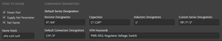
Components that do not fall under these auto-define criteria are treated as normal loads. You can also add named parameters to individual schematic components, defining the type and properties of that component in the power system. These parameters can be specified as part of the component when it is created, or added later in the schematic.
Parameter For Components
For proper recognition, all power-related components should comply with the following criteria:
-
To automatically detect a Source component, the component should have a parameter named Component Type, with the value
Source.
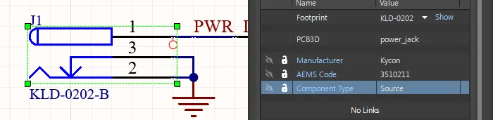
-
If the parameter is not found, the search will be based on Default Connectors Designators, which are defined in the Auto-Define Settings region of the Configuration section in the analyzer document (*.pdnaK). Note that only connectors with power connections will be defined, unless they are referenced as part of an extended net.
-
Voltage Regulator Modules (VRMs):
-
Linear regulators should have a parameter named Component Type, with the value
VRM.
-
For an SMPS-type VRM regulator, the Component Type parameter must have the value
SMPS.
-
If the VRM includes a Sense function, the Component Type parameter must have the value
Sense.
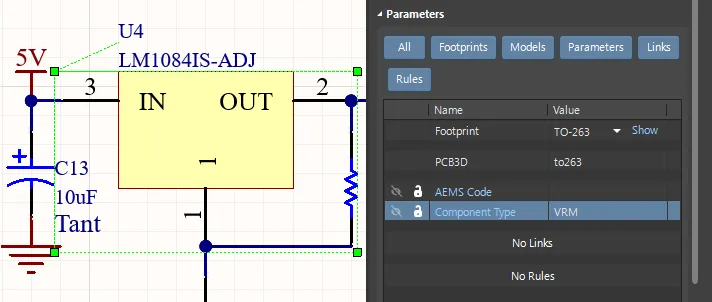
-
If the parameter is not defined, the search will be based on the VRM Keywords defined in the Auto-Define Settings region of the Configuration section in the analyzer document. By default, these keywords are:
PWR, REG, Regulator, Voltage, Switch.
-
The component (Load) consumption value should be defined with a parameter named Current Consumption. Pay attention to the decimal separator symbol used in the value, it could be . or , based on system preferences.
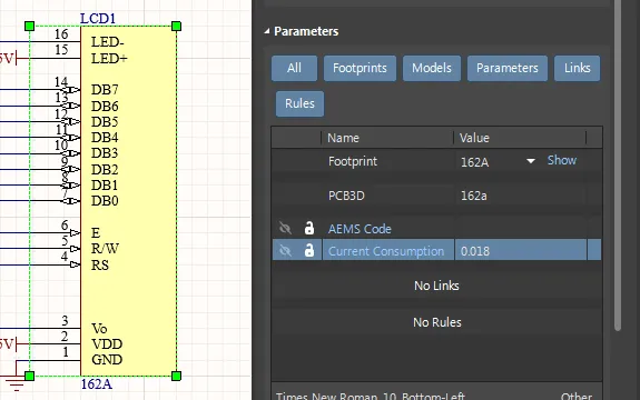
If a component has the Current Consumption parameter, the specified value is divided among all pins connected to the same circuit.
Parameter Synchronization
All parameters must be synchronized between the PCB and schematic. This can be checked by selecting a component on the PCB and confirming that the power analysis parameters are present in the Parameters tab of the Properties panel.
For Design
-
All power nets should be defined:
-
using a Power Port object,
-
have the Power Net property configured so that the net includes the Supply Net Parameter (as described below),
-
or named such that their name is detected by the Name Mask (defined in the Auto-Define Settings region of the Configuration section in the analyzer document).
-
To get a voltage value using the Name Mask, the power net name should comply with the format
*V* or *.*V, where * is a numeric value, as shown in the image below.

-
An alternative way to define the voltage value for the power net is to configure the Power Net property, defined in the Properties panel for any wire in the net. To enable the property, you first place a Parameter Set Directive (Place » Directives » Parameter Set) on the net (hover the cursor over the image below to display an image of this process). The Size, Color and Label are user-defined, it is the presence of the directive that enables the Power Net property of that net. Once the directive has been added, select a wire in that net, enable the Power Net property, and configure the net Voltage, as shown below.
-
Series components should comply with defined designators of resistors, inductors, and custom series components (as defined in the Auto-Define Settings region of the Configuration section in the analyzer document).
-
VRMs should be connected to at least two power nets.
Power Analyzer Commands
The following commands are available from the main menus of the Power Analyzer editor.
Command
|
Summary and Use
|
Tools » Define Automatically
|
Attempts to automatically recognize the topology of the project, based on the current settings in the Auto-Define Settings region of the Configuration section in the analyzer document (*.pdnaK). This command can also be accessed by clicking the Define Automatically button at the top left of the editor. |
File » Load from File
|
Load a saved Power Analyzer by Keysight document (*.pdnaK) into the Power Analyzer editor. |
Edit » Manage Nets
|
Open the Manage Nets dialog, where you select the Power Nets to be analyzed. Ticking a net adds that net to the analyzer document (*.pdnaK). Unchecking a net removes it (along with all child power nets) from the document. This command can also be accessed by clicking the Manage Nets button at the top left of the editor. Learn more about Managing Nets. |
File » Save
|
Save the current Power Analyzer configuration to a Power Analyzer by Keysight document (*.pdnaK) |
File » Save As
|
Save the current Power Analyzer configuration to a Power Analyzer by Keysight document (*.pdnaK) with a new, user-defined name. |
Tools » Measurement Units » mil
|
Configure the Power Analyzer to use Imperial (mils) measurement units. |
Tools » Measurement Units » mm
|
Configure the Power Analyzer to use metric (mm) measurement units. |
Power Analyzer Limitations
At this stage, the Power Analyzer by Keysight does not support:
-
Negative voltages.
-
Embedded components (components placed on an internal layer). Learn more about Designing a PCB with Embedded Components.
