
Direct ECAD-MCAD Design with CoDesigner
What is CoDesign?
Working between the electronic and mechanical design domains brings unique challenges. ECAD and MCAD tools have different design objectives and have evolved down different paths, as well as how they store and manage their data.
But today's designs demand that this challenge be solved - small and complex product enclosures that house multiple, irregular-shaped printed circuit boards - to successfully design these products, the designers must be able to collaborate as they pass design changes back and forth between the ECAD and MCAD domains.
Passing complex and detailed design changes between different design software is much more than just being able to save data in another format. The electronic and mechanical design teams work independently and must be able to transfer changes at any point in their design process. How do you manage the flow of changes back and forth between the teams, without impacting either team's day-to-day design work? The last thing the design teams need is for one team to have to stop work until the other team has accepted their latest change before both teams can proceed.
This collaborative design challenge is solved by CoDesigner, an interface for transferring printed circuit board designs between the ECAD and MCAD design domains.
How it Works
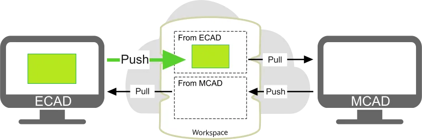
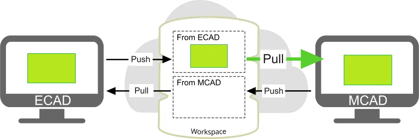
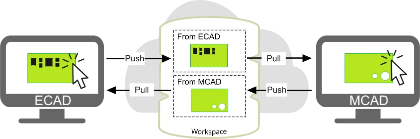
Once the CoDesigner plug-in has been added to the ECAD and MCAD software, CoDesigner can pass design changes back and forth through an Altium Workspace. The Workspace acts as a bridge between the ECAD and MCAD domains, as shown below.

The advantage of passing design changes through a Workspace is the update process becomes stateless. That means each side can continue to work independently, there is no need to worry about where the other team is up to in the design process.
For example, when the MCAD designer has defined the board shape, they can Push the assembly to the Workspace. The ECAD designer will automatically be notified that there is a change pending. When they click Pull, their board is compared to the MCAD board definition in the Workspace, and a list of changes required to synchronize their board with the Workspace version is generated. The ECAD designer can then enable the changes they want, and Apply them to their board. The ECAD designer might then configure the various copper and other fabrication layers required in the layer stack, define the board thickness, and Push the updated board back to the MCAD designer, ready for placement of any location-critical mechatronic components.
What is a Workspace?
An Altium Workspace is a dedicated server for hosting and managing all your design content, that couples directly into your design software. Altium's design software works seamlessly with the Workspace, providing an elegant answer to the question of handling design data with secured integrity.
Altium's design software can connect to the following Workspaces:
- Altium 365 Workspace - a Workspace hosted on the Altium 365 cloud-based infrastructure platform. The Workspace facilitates the seamless connectivity of, and the mechanics for moving data between, the design, manufacturing, and supply domains. A cloud-based Workspace is recommended since it opens up a variety of global sharing and collaborative features that can only be experienced and enjoyed through the cloud-based Altium 365 platform.
- Altium On-Prem Enterprise Server Workspace - if your design team cannot use a cloud-hosted Workspace, Altium also supports an On-Prem Enterprise Server that is installed on-site and managed by your own IT department.
Learn more about Designing with a Connected Workspace
What is a Personal Space?
Every designer who registers with Altium Live also gets access to their own Altium 365 Personal Space. The Personal Space is free, and offers some of the collaborative capabilities available in a Workspace. The Personal Space is also used as the ECAD-MCAD transfer interface for designers working between Altium CircuitMaker and Autodesk Fusion.
Learn more about the Altium 365 Personal Space
Learn more about Collaborating between Altium CircuitMaker and Autodesk Fusion
Transferring the Design Data
The Role of the Workspace
MCAD CoDesigner transfers the design between ECAD and MCAD by Pushing and Pulling design changes through an Altium Workspace. When you perform a Push from ECAD, you are not pushing the PCB file to the Altium Workspace, you are pushing a special ECAD-to-MCAD data package. This package includes: the board data, layer geometry, the component 3D models in Parasolid format (learn more about how the 3D models are named in MCAD), and if enabled, the copper geometry.
When a Push is performed in either ECAD or MCAD, CoDesigner first prepares the data package within a local sub-folder, <DesignName>-EDM. On the MCAD side, the EDM folder is also used to store the MCAD data. This data package is then transferred into a special folder in your Altium Workspace, called Mechatronic 3D Models. This folder is only used by MCAD CoDesigner for storing ECAD-to-MCAD data. If you are using MCAD CoDesigner, please do not delete or move this folder, and do not restrict access for electrical and mechanical engineers.
Learn more about Transferring Mechatronic 3D Models
ECAD-MCAD Object Translations
As the board design is transferred back and forth between ECAD and MCAD, objects in one design space must be translated to equivalent objects in the other design space. For some of the objects, the translation is straightforward; for example, an ECAD mounting hole becomes an MCAD hole, and the MCAD board part becomes the ECAD board shape.
For other objects, the process is not as direct. For example, an ECAD component includes footprint elements that become part of the fabricated board, including the silkscreen and the pads (which include layer-specific details such as copper and solder mask, as well as holes); as well as the 3D model of the component that is loaded onto that footprint during PCB assembly. In MCAD, all of the board-related elements in the ECAD component become part of the MCAD board part, and the 3D model becomes the MCAD component.
This translation of objects can initially result in confusion; for example, when you move a component in MCAD, the component pads and their holes get left behind. After Pushing the board back to ECAD and then Pulling into MCAD again, the location of those pads updates to match the new location of their component.
To help understand this, the collapsible sections below summarize how objects are translated in each direction.
ECAD Board (*.PrjPcb) to MCAD Board Assembly
| ECAD Object | becomes MCAD Object | Notes | |
|---|---|---|---|
| Board | Shape - rigid board region | Part with an extruded sketch of the board shape | |
| Shape - flex board region | Sheetmetal part with the sketch that corresponds to the flex region, with sketched bends for each ECAD bend | ||
| Cutout | Extruded cut feature | ||
Pad hole |
Circular hole | Hole in Board Part |
|
| Circular hole with countersink / counterbore | Hole with countersink / counterbore in Board Part | Uses the MCAD Revolve feature | |
| Slotted hole | Extruded cut feature in Board Part | ||
| Rectangular hole | Extruded cut feature in Board Part | ||
| 3D Object | Both true 3D models & extruded 3D body objects | Not transferred | It is assumed that 3D objects are part of the mechanical enclosure and already exist in MCAD. To transfer mechanical items from ECAD, include them as an ECAD component. |
| Room | Text Note Room extruded surface | Placed and graphically shaped in ECAD as a Room object, configured as a Placement Design Rule | |
| Keepout area | Keep out area extruded surface | Can apply to all layers (defined on ECAD Keep-out layer), or be layer-specific (defined on an ECAD signal layer) | |
| Rout tool path | Extruded cut | ||
| Component | 3D model | MCAD Part Model | Transferred as a Parasolid part, unless MCAD part referencing is enabled and suitable parameter detected, then MCAD part placed from PDM. (learn more) |
| Component Parameters | MCAD Part Properties | ||
| MCAD part reference (optional) | MCAD part from PDM | MCAD part referencing configured in Workspace, and MCAD part reference included in component, and MCAD part found in the MCAD PDM. (learn more) |
|
| With Copper Geometry options disabled (learn more) | |||
| Component | Component copper (pads & user-defined copper areas) (also Free Pad copper) |
Surface layer copper becomes part of the surface Decal | Learn more |
| Silkscreen / Soldermask | Surface Decal | Learn more | |
| Vias | Copper | Surface Decal | Learn more |
| Hole | Ignored | ||
| Barrel | Ignored | ||
| Other Copper, Soldermask & Silkscreen objects | Surface layer Decal for each side of the board | Each Decal combines: Silkscreen, soldermask, surface layer copper (learn more) |
|
With Copper geometry options enabled (learn more) |
|||
| Copper & Soldermask layers | Extruded sketch in <LayerName_ID> Assembly |
Build 3D Copper Geometry option enabled Each copper and soldermask layer becomes an MCAD assembly with an extruded sketch of the objects on that layer | |
| Pads (component and free pads) | Copper | Extruded sketch in <LayerName_ID> Assembly |
Build 3D Copper Geometry option enabled |
| Barrel | Extruded sketch inINTERLAYER<ID> Part |
Build 3D Copper Geometry option enabled (Part is a child of INTERLAYER<ID> Assembly) | |
| Vias | Copper | Extruded sketch in<LayerName_ID> Assembly |
Build Vias option enabled |
| Hole | Hole in Board Part | Build Vias option enabled | |
| Barrel | Extruded sketch inCOPPER_LAYER_VIA<ID> Part |
Build Vias option enabled (Part is a child of INTERLAYER<ID> Assembly) |
|
MCAD Board Assembly to ECAD Board (*.PrjPcb)
| MCAD Object | becomes ECAD Object | Notes | |
|---|---|---|---|
| Board | Extrude based on the board outline shape | Board shape | Circular fillets with a constant radius and symmetric distance-distance style chamfers are supported. (Learn more) |
| Extruded cut | Board cutout | ||
| Internal contour in the board outline sketch | Board cutout | SOLIDWORKS only | |
| Hole | Free pad | ||
| Board cutout | SOLIDWORKS only, when the Transfer board sketch holes option is enabled in the CoDesigner Settings dialog. (learn more) |
||
| Part Model | Component linkage enabled | ECAD Component | If MCAD-ECAD model linkage is configured and the referenced ECAD component is found in the Altium Workspace. (learn more) |
| Component linkage not enabled | 3D Body Object | MCAD part placed as an ECAD 3D Body object (referred to as a Freebody object during Pull into ECAD). Note that changes made to Freebody objects in ECAD (location, orientation, etc) are not transferred back to MCAD. (learn more) |
|
| Assy / Part | Located outside of the PCB Assembly and Defined in CoDesigner as part of the Enclosure, OR, located inside of the PCB Assembly | 3D Body Object | Location changes made in ECAD are not transferred back to MCAD. (learn more) |
| Not defined in MCAD as part of the Enclosure | Not transferred | ||
| Constraints | Board outline | Not modified unless board shape is edited in ECAD, then board is redrawn in MCAD (edge IDs are updated). Constraints applied to those edges will be lost. | Board will remain in location in MCAD, constraints can be restored if required. (learn more) |
| Component | ECAD component is locked | Learn more | |
| Unsupported Changes | Learn more | ||
Automatic CoDesigner Push when you Save to Server
When you perform a Save in ECAD, your design file is saved locally, into the project's working folder. When you perform a Save to Server, your file is saved locally, and then also saved to the project's Workspace folder.
These actions are independent of performing a Push in MCAD CoDesigner. This separation of MCAD Pushing and Saving to Server can be a source of confusion, where an electrical engineer might think that the Save to Server they performed at the end of the day meant that everyone else who needs access to that design data, is now up-to-date and ready-to-go.
To simplify the process of keeping files in sync, after the project has been Pulled at least once into MCAD the Workspace then performs an automatic Push, whenever a Save to Server is performed on the project in ECAD.
 An MCAD Push is automatically performed when the project is Saved to the Server.
When the MCAD engineer performs a Pull, they are alerted to the fact that the last MCAD Push was automatic, as shown in the slides below.
![]()
![]()
![]()
Where MCAD CoDesigner Logs its Operational Progress
MCAD CoDesigner logs extensive details about all aspects of ECAD and MCAD operations into log files. The log files are located in:
C:\Users\<>\AppData\Local\Altium\Altium CoDesigner\
In this location:
-
ECAD events are logged into:
AltiumDesignerExtension.log -
MCAD events are logged into:
<McadName>Addin.log
The Collaborative Design Interface
Both your Altium and your MCAD software interface to each other through a panel (tab) in the software. In your Altium software, it's called the MCAD CoDesigner panel; in your MCAD software, it's called the Altium CoDesigner panel, or tab.
MCAD CoDesigner / Altium CoDesigner Panel
![]()
![]()
-
In your Altium design software, the MCAD CoDesigner panel is used to Push and Pull design changes back and forth, and display messages.
-
In the MCAD software, the Altium CoDesigner panel is used to:
-
Create new collaboration projects
-
Open an existing collaboration project
-
Configure collaboration options
-
Push and Pull design changes back and forth
-
Display messages
-
Working in the CoDesigner Panel
The functionality available in the CoDesigner panel is essentially the same in both ECAD and MCAD. The panel always displays the last change made in ECAD and the last change made in MCAD.
![]() All CoDesign activity is performed through the CoDesigner panel.
All CoDesign activity is performed through the CoDesigner panel.
Latest from ECAD / Latest from MCAD
-
These two sections display the last change made in ECAD and the last change made in MCAD.
-
Click the triangle icon to expand the panel and show the detail of the last change
 .
.
-
When new changes are pushed from the other domain, the
 banner appears automatically, as shown below.
The panel will detail:-
The sign-in name of the engineer who performed the Push
-
The optional comment they entered when they Pushed
-
![]() When changes are pushed, a New Changes notification banner appears.
When changes are pushed, a New Changes notification banner appears.
- When the Pull button is clicked, CoDesigner compares the currently open design against the version last Pushed to the Workspace from the other design domain. Each difference that is detected is listed in the Changes list in the panel, as shown below. When you select a change in the list, the impact of that change is highlighted in purple, if possible.
![]() Click on a Change in the list to highlight the impact of that change.
Click on a Change in the list to highlight the impact of that change.
- Clear the checkbox for each change you do not want to apply.
- There may be a change that cannot be applied. In this situation, that change and its checkbox are greyed out. This difference will continue to exist after the changes have been applied and should be discussed with the engineer who Pushed it.
- When you are ready, click the Apply button to apply all enabled Changes to the currently open design.
Support for Change History and Rejection Comments
The complete history of all changes is retained. To examine the history, click the History link to the right of the Latest from the ECAD/MCAD drop-down, as shown below.
 Change history makes it easy for the engineers on both sides to be aware of each other's responses to the changes being made.
Each set of changes details:
-
Who performed this Push (
 ) or Pull (
 ) event, and from which design domain (
 ECAD, or
  MCAD)
MCAD)
-
The date and time these events occurred.
-
The optional summary statement included when the changes were Pushed from the other domain.
-
A list detailing each specific change, with a tick indicating which change was accepted, or a cross for each change that was rejected.
-
An optional statement detailing why a specific change was rejected.

-
Click the
 button in the History mode of the panel to return to the Latest Changes mode.
-
Click the View Project in Browser button to view the project in your Workspace.
-
In the browser, click the History link on the left to view the project history, as shown in the image below. Each history event tile for a CoDesigner push is titled
MCAD Changes Suggested, and includes the name of the person performing the push, the date and time, as well as the message if one was included. Use this information to cross-reference between the CoDesigner panel and the history view.Learn more about Project History in: an Altium 365 Workspace, or in an Enterprise Server Workspace.
 The history of changes can also be viewed in the Workspace.
PCB Definition - Board Areas
In a design, there may be areas on the board that require special attention, which the MCAD engineer needs to define and pass to the ECAD engineer. For example, there may be a zone on the board surface that must be kept clear of copper because a conductive part of the enclosure comes into contact with the board surface when the product is assembled. To support this, the MCAD engineer can define Keep Out Areas and Text Note Rooms, using the buttons on the Altium CoDesigner ribbon.
If either of these objects has been placed on the board in MCAD, they will be listed in the Board Areas list in the PCB Definitions section of the CoDesigner panel:
-
Keep Out Area - A Keep Out Area defined in MCAD will become a PCB Keepout in ECAD. A PCB Keepout is a region or area of the board that has been configured to restrict the placement of specific ECAD objects. Keepouts can be defined for either side of the board, or applied to all PCB layers. The objects that are to be kept out of this area on the ECAD PCB are selected as Keepout Restriction properties in the Altium CoDesigner MCAD panel; configure them as required. Learn more about placing a Keep Out Area in MCAD.
-
Text Note Room - A Text Note Room defined in MCAD will become a PCB Room in ECAD. A PCB Room is a design rule used to define an area where specific components must be placed in, or excluded from. A common use for this rule is to define a component height restriction in the board area covered by the Room. Typically, the Room rule will be applied to an individual component or a class of components. Click on a Text Note Room definition in the Altium CoDesigner MCAD panel to select it, then enter instructions or information for the ECAD engineer; this text will become the Comment field for that Room in the ECAD PCB editor. Learn more about placing a Text Note Room in MCAD.
![]()
![]()
PCB Definition - Board Enclosure
CoDesigner supports working at the device assembly level in MCAD, and transferring the enclosure with the board from MCAD to ECAD.
![]() CoDesigner recognizes that the board and the enclosure have been added to the device assembly.
CoDesigner recognizes that the board and the enclosure have been added to the device assembly.
Learn more about working in the device assembly and pushing the enclosure from MCAD to ECAD.
CoDesigner MCAD Settings Menu
![]() The CoDesigner settings menu is used to configure CoDesigner in your MCAD software.
The CoDesigner settings menu is used to configure CoDesigner in your MCAD software.
Click the down arrow at the top right of the Altium CoDesigner panel to open the menu.
Use the menu options to:
- Confirm which Server/Workspace you are currently signed in to.
- Sign out of the Server/Workspace you are currently signed in to.
- Open the CoDesigner Settings dialog, where you can configure a central location to store models and enable true copper support.
- Access a Custom Server. Clicking the Use Custom Server option will sign you out of the current Workspace and return you to the sign-in mode of the Altium CoDesigner panel.
The CoDesigner MCAD Ribbon
When the CoDesigner Add-In is installed in your MCAD software, it adds the Altium CoDesigner Ribbon to the interface. Click on the Altium CoDesigner tab to access the Ribbon, which provides an easy way of accessing the common PCB-specific design objects needed during the ECAD-MCAD CoDesign process. Using these buttons ensures that the correct MCAD object type is used to create a compatible ECAD object.
![]() Use the CoDesigner Ribbon to define objects on the PCB in an ECAD-ready way.
Use the CoDesigner Ribbon to define objects on the PCB in an ECAD-ready way.
Recommended Collaboration Workflow
ECAD-MCAD CoDesign is a flexible process, there is no prescriptive approach that must be followed. While it is common for the board shape to be designed in MCAD, the board thickness must be defined in ECAD because that is where the various PCB layer materials are selected and configured. This requirement leads to a recommended design flow, as outlined below.
Starting the Collaboration Process in ECAD
In ECAD:
-
Create the project.
-
Add a PCB.
-
Define the layer stack to set the board thickness.
-
Open the MCAD CoDesigner panel (click the Panels button at the bottom right of the design space and select the panel name, or use the View » Panels submenu),
-
Push the board using the button in the MCAD CoDesigner panel. As well as Pushing the ECAD-MCAD exchange data to your Workspace, this also saves the project and the board file to the Workspace. The saved project and board become the ECAD designer's working files.
Details for Starting the Design in ECAD
Create the Project
The PCB must be part of a project for you to be able to share it with an MCAD designer.


To create a new managed project:
- Select File » New » Project to open the Create Project dialog.
- In the Locations column, select your Workspace.
-
Set the Project Type to
PCB <Default> -
Set the remaining dialog options to:
- Project Name - name of the ECAD PCB project
- Description - optional description of the project
- Folder - the folder where the project is stored in your Workspace
- Local Storage - folder on your hard disk, below which the working copy of the project will be stored (a project folder, named the same as your project, is automatically created)
Add a PCB to the Project
A PCB must be added to the project in ECAD, regardless of where the project was first created.
 A PCB must always be added to the project in ECAD.
Adding a new PCB:
-
Select File » New » PCB, a new blank PCB will be added to the project and opened in the PCB editor.
-
Save the PCB with a suitable name (File » Save).
Define the PCB Layer Stack
The Layer Stack, or Z-plane properties of the CoDesign board, are defined in the PCB editor's Layer Stack Manager.
 The layer stack defines the thickness of the board.
Defining the Layer Stack:
- Select Design » Layer Stack Manager, the Layer Stack Manager editor will open on a separate document tab, as shown above.
- Use the right-click menu to add the required new layers to the layer stack.
-
For each layer, click the ellipsis button (
 ) in the Material column to select the correct layer material from the Material Library.
- Save the Layer Stack to update the PCB with these changes. Click here to learn more about defining the layer stack.
- Save the PCB file and the Project (File » Save All). This saves the working copies of the project files.
- The last step is to save the project files to the Workspace. Right-click on the project name in the Projects panel and select Save to Server from the context menu. The Commit to Version Control dialog will appear, indicating which modified files need to be committed. Enter a comment if required, and click the Commit and Push button.
Push the Board to the MCAD Designer
Assuming that the X-Y shape of the board is being defined in the MCAD software, the board can now be Pushed to the Workspace.
 Now that the thickness has been defined in ECAD, the board can be pushed to MCAD for shape definition.
Pushing the board to the MCAD software:
-
If the MCAD CoDesigner panel is not open, click the
 button (lower right of the software) and select MCAD CoDesigner from the menu.
- Click the Push button in the panel.
- A message window will appear, enter a message for the MCAD designer that describes what you are pushing to them.
- Click Send to complete the Push process. A message dialog will appear, reporting the status of the process.
- When the Push is complete, the Latest from ECAD section in the panel will display the Activity thread, as shown below.
 The Latest from ECAD section reports that the board has been Pushed to the Workspace, note that the panel also reports there have been No Pull actions yet.
In MCAD:
-
Open the Altium CoDesigner panel. The steps to open the panel will depend on which MCAD software is being used; use the relevant Installing CoDesigner in your MCAD software link for more details.
-
Pull the Board in the Altium CoDesigner panel - this creates an MCAD board assembly based on the board definition in your Workspace.
Details for Pulling the board into MCAD
If the project and the board have already been created in ECAD but not yet opened in your MCAD software, the project must be Pulled from your Workspace. To do this:
-
Open your MCAD software.
-
Display the Altium CoDesigner panel. Sign in to your Workspace if you are not currently signed in. If you're not sure how to display the panel, learn more about Installing and Configuring Altium MCAD CoDesigner.
-
Because there is no assembly currently open, the panel will display the Pull, Create, and Recognize Designs buttons. Click the Pull button.
-
The Select Project dialog will open, select the required project and click OK.

-
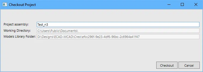
In SOLIDWORKS and Autodesk Inventor, the Windows Save As dialog will appear; save the MCAD assembly in a suitable location.
In PTC Creo the Checkout Project dialog will appear if Creo is connected to Windchill, where the MCAD Project assembly can be renamed if required. It also details the current Working Directory and the Models Library Folder locations. Click Checkout to create the MCAD assembly.
- The board assembly will display in the MCAD editor, ready to be worked on. Save the MCAD design changes as an MCAD assembly.

- When required, design changes can be passed to the ECAD environment by clicking the Push button in the Altium CoDesigner panel.
-
- Insert the board into the device assembly.
- Configure the board shape to suit the enclosure.
- Define the mounting holes.
- Position location-critical mechatronic components.
- Define any required Keep-out Zones or Text Note Rooms.
-
Save the MCAD assembly.
Pushing from MCAD back to ECAD:
- Using the button in the MCAD CoDesigner panel, Push the board to the Workspace - this saves the board definition, holes, and placed component details as MCAD-ECAD exchange data.
Pulling into ECAD:
- Open the board and perform a Pull to load the updated board definition and component details from your Workspace.
In MCAD or ECAD:
-
Reopen the assembly or PCB file to continue working on the design.
Re-opening an Existing Board
To continue working on an existing board design (either ECAD or MCAD), re-open your working copy of the Assembly (MCAD), or project and board file (ECAD). If there are any updates pending the CoDesigner panel will display a warning that New changes have been detected. If the New changes message does not appear automatically, click the Pull button to force CoDesigner to check for changes.
 If the mechanical assembly already exists, reopen it to continue working on the design.
Starting the Collaboration Process in MCAD
- It is possible to start the PCB design process in MCAD, but it is not recommended. The process is the same in all of the supported MCAD environments.
Starting the Design in your MCAD Software
You start the design process in your MCAD software in the Altium CoDesigner panel, by clicking the Create button. However, the flow is not intuitive because, in ECAD, the engineer must still create a PCB file to pull the MCAD board definition into.
![]()
- Sign in to CoDesigner, as described on the relevant page of the Installing and Configuring Altium MCAD CoDesigner section.
- Click the Create button in the Altium CoDesigner panel (also referred to as a tab in some MCAD tools).
- The Select Project dialog will open, click the New Project button in the dialog, as shown above.
- The Create New Server Project dialog will open. In the dialog, enter a suitable Name and optional Description for the project, and click OK. The Windows Save As dialog will open.
- A default board assembly is now being created in the MCAD software, which you need to save in a suitable location. Enter a name, select a location to store the assembly, and click Save in the Windows Save As dialog. The MCAD editor will display the new, default board shape. As part of this step, an ECAD PCB project is also created in your Workspace.
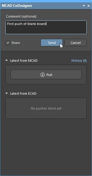
- The new board shape information does not exist in the Workspace yet. To add it, click the Push button on the Altium CoDesigner panel. A Comment window will appear on the Altium CoDesigner panel, this comment will be displayed in the ECAD software.
- Enter a brief description in the Comment window and click the Send button. A message dialog will appear while the changes made to the board shape are being saved to your Workspace. When that process is complete your Push message will appear in the Altium CoDesigner panel.
Push and Share to Invite a Mechanical Engineer (Workspace hosted on Altium 365)
When you click Push in the MCAD CoDesigner panel in ECAD, the MCAD CoDesigner panel also provides the opportunity to Share the project with another engineer.
CoDesigner Pushes and Pulls the board design by passing a special ECAD-to-MCAD data package back and forth through your Altium Workspace. When you enable the Share checkbox, you launch a process that configures Workspace access and project permissions for the invited engineer to access the project, including the special ECAD-MCAD data package. The invited engineer's access is delivered in their MCAD software through the Push/Pull features in the Altium CoDesigner panel, and also through a Web browser if they have or choose to create an Altium Account as part of the invitation process.
The project can be shared with anyone, regardless of whether they are already a member of the project's Workspace, or even have an Altium Account. The table below summarizes the project access, depending on the state of permissions that the invitee had when the Share is performed.
| Existing Altium Account Status | Existing Workspace Status | Permissions Assigned During Share | Notes |
|---|---|---|---|
| No active Altium account | Not a member of the Project Workspace | Given Guest access to the project, with Edit permissions | Invitee receives an email with a link to create an Altium Account. Once created, the Guest will then also have browser access to the Project through the Shared with Me section of their Personal Space. Note that the invitee will not have access to the project from their MCAD software. This can be resolved by adding the user as a member of the Workspace and assigning them Edit permissions. |
| Active Altium account | Not a member of the Project Workspace | Becomes a Member of the project's Workspace and assigned the Mechanical Engineer Role, project shared with View permissions | The new Workspace member is assigned the Mechanical Engineer role. Now that there is a Workspace member with the ME Role assigned, the Share checkbox will no longer be automatically enabled. Note that project permissions must be elevated to Edit for the Mechanical Engineer to be able to perform a Push from MCAD. |
| Active Altium account | Already a member of the Project Workspace | Project shared with Edit permissions |
The Sharing Process
If the Share checkbox is enabled, the Share with a Mechanical Engineer dialog will open when you click the Send button in the MCAD CoDesigner panel.
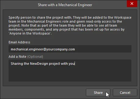
Enter the Email Address of the person you wish to share the project with (and an optional Note), then click the Share button in the dialog. If the invitee is not already a member of the Workspace, the Share with a Mechanical Engineer notification dialog will then appear, warning that the invited user might be outside of your organization.
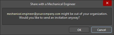
When you click OK in this dialog, or if they are already a member of your Workspace, a notification email is then generated and sent to the invitee.
 ).
).After a brief delay, a success dialog will appear.
The project is now shared with the Mechanical Engineer.
 ).
). )
)
Working Between MCAD and ECAD
At any point in the design process, changes can be transferred between the MCAD and ECAD tools, using the CoDesigner panel.
![]()
 Changes are pushed and pulled between the MCAD and ECAD tools through the CoDesigner panel.
- To transfer design changes, click the Push button in the corresponding panel.
- When the Push button has been clicked, an editing window appears at the top of the source editor's panel. Enter a message about the design change then click Send.
-
When Send is clicked:
- The working copy of the modified PCB file is automatically saved if it is currently unsaved.
- The changes are written to your Workspace.
- The Posted message is displayed in the message thread of the source editor's CoDesigner panel.
- The target editor's panel will display a message that there is a change pending the next time they open their working copy of the design file.
- Click Pull in the target editor's panel, a list detailing each change needed to re-synchronize the designs will be displayed.
Working with the Change List
When the Pull button is clicked, each change that needs to be made to the working file to synchronize it with the snapshot on your Workspace is listed, as shown below.
![]()
- Each difference detected between the current design and the snapshot stored in your Workspace is detailed as a Change in the Change List.
- A Change does not have to be accepted. If a change is ignored it will appear in the Change List again, the next time an update is performed in that direction. Be aware that if you choose to ignore a change, for example moving a mounting hole, and you then perform a Push of your design changes, the ignored change may be overwritten since your version has the mounting hole in the old location. The MCAD designer can always avoid losing their change by not accepting your mounting hole move.
- A single design change, such as changing the location of a component, can become multiple changes in the Change List. When a PCB component is moved, there are MCAD changes to: the location of the component, the shapes the component makes on the Component Overlay, and the shapes the component makes in the top and bottom copper layers. Related changes should all be applied together.
- The list may include changes that cannot be applied in the target environment. In this situation, the change will be displayed but the checkbox will be unavailable, indicating that this difference cannot be resolved.
- Where possible, the selected change is highlighted in the design space when you click on it in the Change List.
- Click Apply to apply the changes that are ticked.
MCAD-Coordinates Grid
CoDesigner uses the ECAD Absolute Origin as the reference when the board is pushed from ECAD to MCAD. CoDesigner 2.4 introduced a feature to create a new MCAD Coordinates grid on Pull into ECAD, including an MCAD Origin entity, when the MCAD origin differs from the default (absolute) ECAD origin. This helps the electrical engineer communicate with the mechanical engineer on the positioning of the different board entities.
The representation of the MCAD Coordinates grid can be customized in ECAD, double-click on the entry in the Properties panel to open the Grid Editor dialog. Learn more about the PCB Grids System.
 The coordinate grid defined in MCAD can also be customized in ECAD.
MCAD Planes for Component Placement
From CoDesigner 2.2.0 onward, top and bottom side component planes are created in MCAD when the board is pulled, to simplify the process of placing components in MCAD. Components pushed from ECAD are placed in MCAD to ignore the thickness of the solder mask layer.
![]()
How CoDesigner Handles Copper, Mask and Overlay Layers
Along with the board shape and components, CoDesigner also transfers the top and bottom side: copper, solder mask, and component overlay layers, from ECAD to MCAD.
ECAD Layers as Decals
The default is that these layers are Pushed to the Workspace from ECAD as individual SVG images. When the board assembly is Pulled into MCAD, CoDesigner converts the SVG images to PNG images. From these PNG images, CoDesigner then combines the top-side set of images into a single top-side decal, and the bottom-side set into a single bottom-side decal. These two decals are then applied to the top and bottom board surfaces during Pull into MCAD.

 The top and bottom side decals are applied to each side of the board in MCAD.
Autodesk Fusion - ECAD Layers as Sketch Profiles
A different approach is used to transfer the top/bottom copper and component overlay layers from ECAD to Autodesk Fusion. In Autodesk Fusion, these layers are imported as Sketch Profiles drawn on the Board object. This set of layers can be toggled on and off in Autodesk Fusion by clicking the Advanced Geometry ( ![]() ) button in the Altium CoDesigner ribbon. Alternatively, use the Autodesk Fusion visibility icon to selectively hide/display any of these layers.
) button in the Altium CoDesigner ribbon. Alternatively, use the Autodesk Fusion visibility icon to selectively hide/display any of these layers.
 Component overlay and surface copper layers are created as Sketch Profiles in Autodesk Fusion.
Advanced Copper Geometry in MCAD
As an alternative to displaying decals (images) of the copper + mask + overlay layers in MCAD, CoDesigner can also transfer the actual copper geometry (referred to as Advanced Copper Geometry) and the 3D mask layers to MCAD. This feature is currently supported by PTC Creo, Autodesk Inventor, SOLIDWORKS, and Siemens NX. From CoDesigner 2.7 onward, the component overlay (silkscreen) decal is applied to the face of the solder mask extrude.
 The copper layers can be transferred to MCAD if required. In the image above, the components and the layers have been hidden, except for the top copper layer.
To include the Advanced Copper Geometry, enable the Build 3D geometry for Copper and Solder Mask option in the Altium CoDesigner Settings dialog (along with the Build Vias option if required). The Settings dialog is accessed from the CoDesigner menu in the Altium CoDesigner panel ( ).
).
.") Enable the Build 3D geometry for Copper and Solder Mask option to include these layers in the MCAD assembly (Autodesk Inventor dialog).
Enable the Build 3D geometry for Copper and Solder Mask option to include these layers in the MCAD assembly (Autodesk Inventor dialog).
Notes about working with copper geometry and 3D mask layers:
- Copper and mask layers are included as MCAD sub-assemblies.
- All PCB copper layers that are present in the layerstack are included. Note that the copper layer thickness does not include plated layer data, such as Surface Finish. This will be added in a future update.
- Thruhole pad barrels are included when the Build 3D geometry for Copper and Solder Mask option is enabled.
- The via surface shapes are also included when the Build 3D geometry for Copper and Solder Mask option is enabled. Enable the Build Vias option to include the via copper barrels.
- When the Build 3D geometry for Copper and Solder Mask option is enabled, the component overlay (silkscreen) decal is applied to the face of the solder mask extrude.
- Depending on the complexity of the design, including the copper geometry and vias can significantly increase the file size and the time to Pull the design into MCAD.
- Copper and mask data is always Pushed from ECAD. There is no need to Push again from ECAD if you enable the Build 3D geometry for Copper and Solder Mask and Build Vias options in MCAD, just close the board and Pull it again from the Workspace.
Accurate Representation of the Solder Mask
Introduced in Update 2.5, CoDesigner builds a precise model of the solder mask, including the openings for the pads, as a separate entity in MCAD when the Build 3D Copper option is enabled. Because the mask fills the etched regions between the copper, the thickness of the mask layer in MCAD is the sum of the thicknesses of the top copper layer plus the solder mask layer, as defined in ECAD.
 Since the solder mask fills the etched regions between the tracks, pads and vias, its total thickness in MCAD is the sum of the copper layer thickness plus the solder mask thickness, as defined in ECAD.
Support for Keepouts and Rooms
The Altium CoDesigner Ribbon provides an easy way of accessing the common PCB-specific design objects in MCAD, including Keepouts and Rooms. Using these buttons ensures that the correct MCAD object type is used to create a compatible ECAD object.
![]()
Support for Keepouts
A PCB Keepout is a region or area of the board that has been configured to restrict the placement of specific ECAD objects. Keepouts can be defined for either side of the board or applied to all PCB layers. The objects that are to be kept out of this area are selected as Keepout Restriction properties.
Defining a Keepout in MCAD:
- Click the Keep Out Area button on the Altium CoDesigner ribbon.
- You will be prompted to choose a face, surface or plane, click on the side of the board that requires the keepout. If the keepout is to apply to all layers it can be drawn on either side.
- Click on a suitable MCAD sketch tool, such as Rectangle, to define the keepout. Note that the sketch must only include one contour; internal contours are not supported.
- Draw the shape required for the keepout.
- Exit the Sketch mode.
- The properties of the feature can now be edited. You can think of the keepout as a fence around the keepout area, edit the Depth to a small value, for example, 1mm.
- This keepout will become an ECAD layer-specific keepout, on the layer it has been drawn in MCAD. To define an all-layer keepout, in MCAD configure the keepout to extrude in both directions, setting the Depth in the second direction to a value that is large enough to extrude it through the board.
-
Click the MCAD Accept button
 to finish the feature definition process. If required, the feature can be renamed in the Feature tree.
- In the Altium CoDesigner panel, select the PCB Definition tab and configure the keepout restrictions as required. The keepout can now be pushed to ECAD, where it will be added as a Keepout Region. Depending on how it was configured in MCAD, it will become a Top Layer Keepout, a Bottom Layer Keepout, or a Keepout Layer Keepout. If required the keepout shape can be adjusted in ECAD and pushed back to MCAD.
Support for Rooms
A PCB Room is a design rule that defines an area where specific components must be placed or excluded. A common use for this rule is to define a component height restriction in the board area covered by the Room. Typically, the Room rule will be applied to an individual component or a class of components.
Defining a Room in MCAD:
-
Click the Text Note Room button on the Altium CoDesigner ribbon.
-
You will be prompted to choose a face, surface or plane, click on the side of the board that requires the room.
-
Click on a suitable MCAD sketch tool, such as Rectangle, to define the room. Note that the sketch must only include one contour; internal contours are not supported.
-
Draw the shape required for the room.
-
Exit the Sketch mode.
-
Click the MCAD Accept button
to finish the feature definition process. If required, the feature can be renamed in the Feature tree.
-
In the Altium CoDesigner panel, select the PCB Definition tab and enter a comment for the room that explains its purpose to the ECAD engineer. The room can now be pushed to ECAD, where it will be added as a Placement Room design rule, on the layer it has been drawn in MCAD. The only property that can be transferred between MCAD and ECAD is the Comment, which becomes the Placement Room design rule comment.
-
The Placement Room design room can now be configured as required in ECAD.
![]() Keepout areas and Rooms can be defined in MCAD and pushed to ECAD.
Keepout areas and Rooms can be defined in MCAD and pushed to ECAD.
Controlling the Number of Components Pulled to MCAD
To improve performance when working on boards with a large number of components, CoDesigner supports excluding components below a user-defined height during a Pull from ECAD. For the height threshold, CoDesigner uses the height defined as part of the component properties in ECAD. Note that this is the PCB component Height property, not the height of the 3D model added to the component footprint ( ).
).
The threshold height that CoDesigner tests for is defined in the Altium CoDesigner Settings dialog, as shown in the image below. The dialog is accessed via the Altium CoDesigner panel in MCAD, select Settings in the panel's menu to open the dialog. The image below shows the settings for Autodesk Fusion, the same setting is available in each supported MCAD.
 Small components can be excluded during Pull to MCAD by setting the Ignore components smaller than the height threshold.
Configuring the Component Height in ECAD
The video below demonstrates techniques for locating PCB components without their Height defined (default of zero) and quickly updating the Height value for multiple components. It then demonstrates how to set the Ignore components setting smaller than in MCAD, and how MCAD CoDesigner handles this during a Pull from ECAD.
Incorrect component Height values can be quickly detected and resolved in ECAD.
Smart Sketch Changes in MCAD
Consider the situation where the ECAD engineer needs to modify the board shape, and that shape has dimensions and constraints applied in MCAD. Previously, the dimensions and constraints in MCAD's sketch would be lost when the board was Pulled back into MCAD. Now during a Pull, CoDesigner redraws only the elements of a sketch which were changed in ECAD, so that the dimensions and constraints related to non-changed elements are kept as they were.
Note that in some cases, for example where there are complex mechanical constraints, this behavior may lead to unexpected changes in the geometry. In such cases, it may be more efficient to disable this new smart sketch support feature and Pull again, then recreate the dimensions and constraints (as was required in earlier versions of CoDesigner). That can be achieved by disabling the Smart Sketch Change option in the MCAD Altium CoDesigner Settings dialog.
Smart dimensions that are not impacted by design changes, are retained during a Pull from ECAD.
Managing the PCB Route Tool Path in MCAD
A common feature of a board design is to define a milling path around the outer edge of the board shape. This path often includes a number of rows of small holes (referred to as "mouse bites"), whose surrounding material is sufficient to hold the board shape within the panel that it is fabricated on. Once PCB assembly is complete, the board can be snapped out of the surrounding waste material.

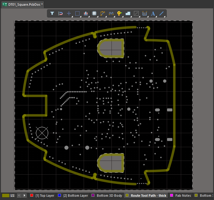
While the route tool path is essential for fabrication it is often not required during MCAD design, when the mechanical engineer needs to focus on fitting the board into the product enclosure. The MCAD CoDesigner 3.13 update saw the introduction of the Build Route Tool Path option to the Altium CoDesigner Settings dialog, giving the mechanical engineer control over whether the Route Tool Path is pulled into MCAD (note that the path is always pushed from ECAD).
 Choose if the Route Tool Path is to be included in the pull into MCAD.
CoDesigning a PCB with Variants
Altium Designer allow the electronics designer to create variations of the product they are designing. Supported variations include: flagging a component as not fitted; modifying a component's parameters, including the component value that is silkscreened on the board; or replacing a component with an alternate component (which may or may not use a different footprint).
In Altium Designer, there is only one board design. Variant information, such as details about an alternate component, is stored in the project file and applied to the board when the variant is selected in the Projects panel. The [No Variations] version of the board is saved as the PcbDoc.
 Altium Designer can be used to create variations of a board design, select the variant in the Projects panel then Push to MCAD in the CoDesigner panel.
Working with PCB Variants
Pushing a Variant from ECAD
When a board is pushed from ECAD, all variants are pushed. The required variant is selected during the pull into MCAD.
 Double-click in the Projects panel to select the required variant to be Pushed.
Pulling a Variant in to MCAD
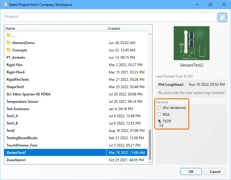
A PCB variant is Pulled to MCAD in the same way as a non-variant PCB, by clicking the Pull button in the Altium CoDesigner panel. If the project includes variants they will be listed in the Select Project dialog, as shown below. Select the required variant and click OK.
If the board is a variant, additional information detailing the variant name is displayed at the top of the Altium CoDesigner panel, as shown below.

Notes about variants:
-
All components, including non-varied and varied components, are identified by the current component model naming scheme.
-
The board part in each variant is identified as :
<DesignName>_<VariantName>_BOARD -
It is recommended to include the variant name as part of the MCAD assembly name.
![]()
![]()
Pushing a Variant from MCAD
In MCAD, CoDesigner is aware if a component is part of the base design [No Variations], or belongs to a specific variant. Changes made to a component in the base design [No Variations] will impact all variants of the board in ECAD, while changes made in a specific variant will only be applied to that variant in ECAD.
Modifications made to a variant are pushed from MCAD to ECAD in the usual way, by clicking Push in the Altium CoDesigner panel.
Pulling a Variant into ECAD
If you attempt to perform a Pull in to the ECAD PCB editor and the wrong variant is currently active, you will receive the following error message. The applicable variant name is displayed in the Error dialog; switch to that variant and Pull again.
 The Pull cannot be completed as the wrong variant is active in the ECAD PCB editor.
If there have been changes made to a component in the base design, they can be applied in any variant in ECAD. Those changes will then be present in all variants in ECAD.
Learn more about working with Variants in ECAD
Recommendations for the Mechanical Engineer
This section details functionality and behaviors that the mechanical engineer should be aware of when using CoDesigner.
Displaying the ECAD Reference Designator in MCAD
Altium MCAD CoDesigner uses a different approach to display the reference designator in Each MCAD tool:
-
Autodesk Fusion – Display the ECAD Properties panel to display the properties of the currently selected part (
 ).
).
-
Autodesk Inventor – Reference designator is displayed in the Model Tree by default (
 ).
).
-
PTC Creo – In the Model Tree mode of the panel, click the Tree Columns button to open the Model Tree Columns dialog. Set the Not Displayed Type to
ECAD Params, locate theECAD_REF_DESparameter, and click the Add Column button ( ).
).
-
SOLIDWORKS – Reference designator is displayed in the Model Tree by default (
 ).
).
-
Siemens NX – In the Assembly Navigator, right-click where the column names are displayed to open the context menu, then select Columns » Component Name to display the Component Name column (
 ).
).
Synchronizing Changes Between Mechanical Engineers
-
CoDesigner transfers the mechanical PCB assembly to ECAD through an Altium Workspace, such as an Altium 365 Workspace. The changes Pushed/Pulled through the Workspace are directional - the PCB assembly Pushed from MCAD (and Pulled to ECAD) is stored separately in the Workspace from the PCB assembly Pushed from ECAD (and Pulled to MCAD). That means a second mechanical engineer cannot Pull the modified board that a mechanical engineer just Pushed to the Workspace, instead they will be Pulling the last-pushed ECAD data. Note that MCAD constraints exist only in the MCAD assembly in which they were created. When the board is pushed from MCAD to ECAD, the component positions resulting from the constraints are pushed, but not the constraints themselves. Therefore if the board is pulled into a new MCAD assembly, none of the constraints created by a previous MCAD engineer will be included.
 ECAD and MCAD changes are stored separately in the Workspace.
To allow other mechanical engineers to see your changes, save your PCB assembly in the same way as you do for any other assembly - to common storage available for both. This method will preserve any MCAD constraints. Alternatively, get the ECAD designer to Pull the data into ECAD, save it, and then Push the updated design back to MCAD. However, as explained above, no MCAD constraints will be included by using this method.
- Another important point is that changes made to the same PCB assembly by different mechanical engineers are not merged when they are Pushed, the latest change Pushed by any mechanical engineer will overwrite previous changes Pushed by other mechanical engineers.
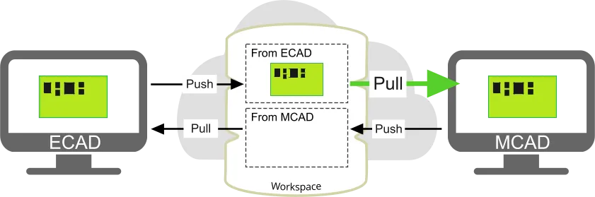
Pictorial Demonstration of the Synchronization Process
ECAD and MCAD push their changes to different storage locations on the Workspace. That means each engineer can only pull changes that have been pushed by the other engineer. Those changes will only include their own changes if they’ve already been accepted by the other engineer before the other engineer has pushed.
For example, a board is created in ECAD, Pushed to the Workspace, and Pulled to MCAD:

If the ECAD engineer then adds components AND the MCAD engineer adds holes, AND if each Pushes their board then Pulls the other’s board, CoDesigner will try to remove the holes in the MCAD engineer's board, and remove the components on the ECAD engineer's board:
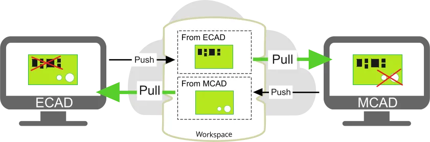
Each engineer does have the option to reject specific proposed changes, for example, the ECAD engineer could accept the addition of the holes but reject the deletion of the removed components. However, working in this way can be hard to manage with complex boards and/or changes. Another point is that all changes to the decals are only seen by CoDesigner as a single change, so can only be accepted or rejected as a whole, not individually.
A better approach is for one engineer to make their changes and push the board, then for the other engineer to pull the board before making their changes, as shown below.


Including Fillets and Chamfers in the Board Shape in MCAD
A common approach for a mechanical engineer is to apply chamfers and fillets to shape the corners of the board. If these are defined in MCAD as 3D entities, CoDesigner cannot transfer them to ECAD because the ECAD PCB editor defines the board shape as a 2D object (with a thickness). To resolve this, when CoDesigner detects such a 3D entity, it offers to convert them to 2D entities and embed them into the board sketch.
 3D MCAD fillets and chamfers applied to a z-axis edge can be transformed to 2D by CoDesigner, and pushed to ECAD.
Fillet and chamfer support:
-
Regular (circular) fillets with a constant radius are supported (
 ).
).
-
Chamfers defined by equal distances from the edge (symmetric distance-distance) are supported (
 ).
).
-
Chamfers defined as an angle-distance (
 ), or non-symmetric distance-distance, are not supported.
- Fillets and chamfers defined on non-straight side edges, as well as on other fillets and chamfers, are not supported.
- Fillets and chamfers defined on a rigid-flex design are not supported.
The Fillet and Chamfer Transformation Process
-
When you click Push to ECAD in the Altium CoDesigner panel and 3D entities are detected, the following dialog is displayed.

-
If you click Yes - the 3D entities are transformed into 2D entities and applied to the board sketch. Note that CoDesigner has not performed the Push yet. The following dialog will appear, instructing you to Push again to transfer the design to ECAD. Visually confirm that the transformation has been performed correctly, then click Push to ECAD in the Altium CoDesigner panel to continue the collaborative design process.

-
If you click No - the 3D entities are not transformed and the following dialog is displayed, listing all 3D entities that will not be transferred to ECAD. This dialog is also displayed when there are 3D entities that CoDesigner cannot transform to 2D.
-

Resolving Issues with the Board Contour in ECAD
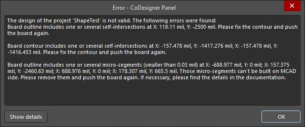
When the board is Pushed from ECAD, CoDesigner checks the board contour and warns the user if there are issues with micro-segments, or if self-intersecting contours have been found. When the board is Pulled to MCAD, CoDesigner will attempt to resolve these issues. If they cannot be resolved, they must be resolved in ECAD.
Automatic Micro-Segment Removal
CoDesigner 2.4 introduced an automatic feature to detect and resolve micro-segments in the board outline. If they are detected, a dialog will appear offering to resolve the issues, as shown below. If you click Yes the detected issues will be resolved automatically. If you click No and close the dialog, an error dialog will then appear detailing the location of any issues, which must then be resolved manually (as described below).

Manual Micro-Segment and Self-Intersection Removal
Micro-segments and self-intersections that have not been resolved automatically or are detected in a board cutout, must be resolved manually.
To fix the issues in ECAD:
-
Copy the error information from the dialog into a text editor so the coordinates for the issues are available.
-
Set the snap grid (Gtrl+G shortcut) to a small value (eg 0.001 mil) so you can make small changes to the location of vertices.
-
Switch to View » Board Planning Mode.
-
Zoom in to the location of the issue. Alternatively, use the Jump Location command (Edit » Jump » New Location, or J, L shortcut) and type the coordinates into the Jump to Location dialog. Note that you can include the units (
mmormil) with the value if they are different from the current board units. If the issue is due to an arc, the issue location could be the arc center point. In this situation visually check the board outline for short, shallow arcs. -
Run the Design » Edit Board Shape command (D, D shortcut). The board outline will display vertices at the ends and center of each edge. Check for multiple vertices that are very close together and very shallow arcs. Use the following tips to help you resolve issues:
- Click and drag on an edge or a vertex to modify the shape. There are three shape modification modes available during editing: Break edge, Move (slide) edge, Incurvate (bend) edge; press Shift+Space during editing to cycle through the modes. The current mode is displayed on the Status bar.
- Move the vertex at the end of a short edge slightly, then release the mouse button. Often this will be sufficient for the software to resolve and remove the short edge.
- A short shallow arc can be converted to a straight edge by dragging the center vertex in Incurvate mode to flatten the arc (it will be replaced by a straight edge when you release it).
- Green alignment guides will display when the moving edge or arc chord aligns with an existing edge.
- Click and hold on a vertex then press Delete to remove it; to add a vertex hold Ctrl as you click on the edge, then position the cursor and release.
-
Push the board again.
Board contour self-intersections and micro-segments must be resolved before the board can be pushed to MCAD.
Learn more about the Vertex Editing Modes
Learn more about Defining the Board Shape
Pull a Previous Revision of the PCB into MCAD
To Pull the ECAD board into an empty MCAD assembly, click the Pull button in the Altium CoDesigner panel to open the Select Project from Company Workspace dialog. The dialog defaults to giving you the last-pushed board. If you need to open a previous release or revision of a PCB design, click Change in the ECAD Push to Open section of the dialog, opening the Select Push dialog.
The dialog lists all previous Pushes, choose the one you require and click OK. If the ECAD commits have been tagged, you can quickly filter the list by enabling the Only show tagged commits option in the Select Push dialog.
 Use the Select Push dialog to select the previous revision, from all revisions Pushed in ECAD.
Visibility of Changes Made on the ECAD side
It is important to open the PCB assembly itself in your MCAD software, not the parent device/assembly that the PCB assembly is being designed to fit in. If the PCB assembly is opened, changes made and pushed from the ECAD side will be detailed in the Altium CoDesigner panel. Changes will not be detailed in the panel if the parent device/assembly is opened.
Getting Changes to your PCB Assembly from ECAD
- Open your PCB assembly as a separate file (as a root assembly) in MCAD.
- Open the Altium CoDesigner panel.
- Click Pull.
- Review the changes in the table, enable the ones you want to be applied, and click the Apply button.
When you have a PCB Assembly Open in MCAD for the First Time
- Add the PCB assembly to your device’s assembly.
- Secure it by applying suitable mates/constraints.
If a contour of the PCB does not correspond to the shape of your enclosure:
- Start editing the Board part.
- Edit the sketch of the board’s extrusion and adjust its shape to the enclosure.
Making Changes to the PCB Design in MCAD
Below are some tips for ensuring the design shapes and objects used in MCAD will be supported when the board is pushed to ECAD.
Editing the board outline shape
- Start editing the Board part.
- Edit the sketch of the board’s extrusion.
Changing the MCAD Board Origin
- If necessary, the mechanical engineer can change the MCAD origin of a bare board in the early stages of the board definition. To do that, the mechanical engineer can simply move or redraw the entire sketch of the board outline, within the board part. Note that the board part is constrained as “fixed” within the board assembly, with its origin coincident with that of the assembly (therefore, the “MCAD origin” relates to both the board part origin and the board assembly origin).
Creating/editing Mounting Holes
- Start editing the Board part.
- Create/edit a Hole feature on the top or the bottom surface of the board part.
Creating/editing Cutouts
- Start editing the Board part.
- Create/edit an Extruded Cut feature based on the top or the bottom surface of the board part.
Editing the placement of components
- Start editing the Board assembly.
- Move/rotate/flip, or mate/constrain a component.
Synchronizing Fixed or Constrained in MCAD to Locked in ECAD
If a component is fixed or constrained in MCAD, it becomes locked in ECAD (regardless of if that constraint allows any movements within the PCB assembly or not). If a component is locked in ECAD, it becomes fixed in MCAD unless it is already constrained there. Changes in the locked/fixed state are synchronized between MCAD and ECAD.
Transferring ECAD Component Parameters to MCAD
ECAD PCB component parameters are transferred to the corresponding models created in MCAD. Note that this does not include components that were originally placed in MCAD.
Working with Constraints and Dimensions in MCAD
Constraints applied to the board outline
- The mechanical engineer can apply a constraint from an element of the board outline: to another board outline element; to a datum/reference feature; to a part in a higher-level assembly; or to a component. CoDesigner does not modify these constraints. However, if the board outline is changed on the ECAD side, the sketch of the board part will be redrawn in MCAD, and all of the edge IDs will be changed. Note that any change to any part of the board outline in ECAD will result in the entire board being redrawn in MCAD, and all board edge IDs changing. If there was a constraint applied to those edges or to the derived surfaces, those constraints will be broken. The board will stay in place in MCAD, and if necessary, the constraints can be manually restored.
Constraints applied to the components
- The mechanical engineer can apply a constraint from a component: to the board; to an enclosure; or to another component. These constraints will stay healthy if the model of that component can be found locally (if the PCB assembly is not built from scratch in a different folder, or if a common folder is set up for storing models). However, if a component is moved on the ECAD side, the placement change on the MCAD side may not correspond to that movement and should be checked manually (CoDesigner will notify you in this situation). For components with an ECAD footprint, the component standoff (location relative to the board surface in the Z direction) will always be defined by the position of the STEP model in the footprint. CoDesigner will always attempt to override any conflicting MCAD constraints on a Pull into MCAD.
Changes that will not be Transferred from MCAD to ECAD
-
Bare Board thickness - defined by the Layer Stack in ECAD.
- 3D Fillets defined with a constant radius and 3D Chamfers defined by equal distances from the edge (defined in the z-axis direction) are supported, as well as holes and extruded cuts in the board's z-axis direction. Any additional 3D geometric features applied to the board part, such as angle-distance chamfers, are ignored. Learn more about working with fillets and chamfers.
- Any additional geometric features applied to the board part (eg. 3D chamfers/fillets), except for holes and extruded cuts in the board's z-axis direction..
- Any additional geometric features created in the context of the board assembly (eg. holes created in the context of an assembly), unless these features are propagated to parts.
- The location of component holes if they are moved separately from the component.
- The size of component holes.
- Feature Patterns.
- Sketches of cutouts with multiple contours (in PTC Creo and Autodesk Inventor).
- Changes made to the extruded copper.
- Changes made to the silkscreen.
- Component deletions. Since component positional changes are transferred to ECAD, the MCAD engineer could indicate a deletion by moving the component outside of the board area (learn why component deletions are not supported).
Working in the Context of the Device Assembly
In CoDesigner 2.2.0, support was added for working at the device assembly level in MCAD, and then transferring the enclosure together with the board to ECAD. The video below demonstrates the process of including the board assembly in the device enclosure, and transferring the enclosure to ECAD.
An overview of working in the context of the device assembly.
Tips for working with the enclosure:
-
After placing the board assembly in the enclosure, click the Recognize button in the Altium CoDesigner panel. CoDesigner will detect the relationship between the board and the enclosure, and detail the names of all board assemblies added to the device enclosure at the top of the panel.
-
Once the relationship has been detected, the last step is to add the enclosure to the board. To do this:
- Select the enclosure in the model tree.
- Display the Altium CoDesigner ribbon.
- Click the Enclosure button on the ribbon.
- Open/display the Altium CoDesigner panel, where you can confirm that the enclosure is associated with the board in the Board Enclosure section of the Altium CoDesigner panel.
-
The enclosure with the board can now be pushed to ECAD.
Sending the PCB Assembly with your Changes to ECAD
- Make sure your PCB assembly is opened as a separate doc (as a root assembly) in MCAD.
- Go to the Altium CoDesigner panel.
- Click Push.
Working with an MCAD Data Management System
CoDesigner supports the placement of native MCAD components when the PCB is being Pushed from ECAD and Pulled into MCAD. To do this, CoDesigner asks the MCAD software to get the model of the component from the MCAD's data management system (by the model’s name) and then places that component on the MCAD PCB assembly, instead of the model that came from ECAD.
ECAD-to-MCAD native component linking is currently supported in:
- PTC Creo Parametric with CoDesigner Addin version 2.6.0, or later, connected to a PTC Windchill® server. Consult your Creo documentation for information on how to connect to Windchill. Learn more about configuring PTC Creo.
- SOLIDWORKS with CoDesigner Addin version 2.6.0, or later, connected to SOLIDWORKS® PDM Professional. Consult your SOLIDWORKS documentation for information on how to connect to SOLIDWORKS PDM. Learn more about configuring SOLIDWORKS to work with native MCAD components.
- Siemens® NX™ with CoDesigner Addin version 3.4.0, or later, connected to Siemens Teamcenter PLM. Consult your Siemens NX documentation for information on how to connect to Teamcenter PLM. Learn more about configuring Siemens NX to work with native MCAD components.
Working with SOLIDWORKS PDM
Placing Native MCAD Components from SOLIDWORKS PDM
When the board design is transferred from ECAD to SOLIDWORKS MCAD, CoDesigner supports replacing the ECAD component with a native MCAD-equivalent component from the SOLIDWORKS PDM system. To achieve this, you must configure settings in:
- MCAD - configure your PDM settings, CoDesigner model storage, and understand the synchronization requirements, as described here.
-
ECAD - reference the MCAD model in the ECAD component, using the correct syntax. The MCAD component reference must be defined in the ECAD component as a parameter, with the parameter value in the form:
<vault>:folder\folder\component.sldprt, where<vault>is the name of the SOLIDWORKS PDM vault. - Workspace - configure the Workspace options to indicate that you want to use native MCAD components, and define which ECAD component parameter will be used to reference the equivalent MCAD component. Learn more about Linking from the ECAD Components to the MCAD Components.
Before Pulling Changes to the Existing PCB Assembly
- Synchronize the local copy of the Common folder for storing models component folder with the server (use the Get latest version command in SOLIDWORKS PDM)
-
Check out the following files:
- Board assembly
- Board part
- For rigid-flex 2.0 assemblies - all of the board parts and sub-assemblies
- If 3D copper is built - assemblies and parts related to the 3D copper and solder mask
- Decal PNGs, if they are stored in PDM
Note: Normally, there is no need to check the component models out of PDM.
On Pulling Changes from ECAD to MCAD
- Pay attention to any changes to component properties which CoDesigner may want to make - the corresponding string will be highlighted in yellow in the list of changes table in the Altium CoDesigner panel in SOLIDWORKS.
A common reason there may be changes is that when creating the component models in MCAD, CoDesigner writes the component properties stored in ECAD’s component library to the MCAD model properties. However, some of those properties, for example, Description and Material, may be changed by MCAD or PDM automatically afterward. Accordingly, if different values of properties are detected, CoDesigner will suggest changing them.
However, if you try to apply those changes, MCAD will require checking each affected model out of PDM or saving them with another name. To avoid this, uncheck those changes related to changing component properties in the Altium CoDesigner panel. Note that it is strongly recommended that you clarify why the component properties are different, and synchronize them on the MCAD and ECAD sides.
After Applying Changes
- Check the newly created components, board assembly, subassemblies and parts into PDM.
Cloning the MCAD PCB
Do you have an existing MCAD PCB assembly that you would like to clone and re-use in a new PCB project in order not to lose your mechanical dimensions and references? This can be achieved by editing two of the properties in the cloned copy of the MCAD assembly.
The MCAD PCB assembly is associated with the ECAD project through two properties, ManagedProjectGUID and ManagedProjectName, which can be viewed and edited in the Properties dialog for the MCAD PCB assembly. The image below shows the Properties dialog for SOLIDWORKS.
 Two properties link the MCAD assembly to the ECAD project.
- To associate an existing MCAD PCB assembly with a new ECAD project, you need to update these properties in the MCAD assembly to suit the new ECAD project.
-
ManagedProjectName- the ECAD PCB project filename:<ManagedProjectName>.PrjPcb -
ManagedProjectGUID- to find the GUID, you can either copy it from the:-
Workspace browser address bar – open the Altium Workspace where the project is stored, then double-click on the project to open it in a separate browser tab. The URL in the browser address bar includes the
ManagedProjectGUID( ); or the,
-
ECAD project file – open the project file in a text editor (it has the
.PrjPcbextension). TheManagedProjectGUIDis located in the[Design]section at the top of the file ( ). Copy the
 ManagedProjectGUID, but do not modify or save the file.PrjPcbin the text editor.
-
-
In your MCAD software, open the MCAD PCB assembly, edit the Value of those two properties, save the MCAD assembly, and close it.
-
Reopen the clone MCAD assembly and check the top of the Altium CoDesigner panel; it should now display the
ManagedProjectNameproperty that you entered into the clone file in step 1. If it does, then the cloning process has been successful, and the board definition can now be Pushed to the Workspace from your MCAD software. After editing the
 ManagedProjectNameandManagedProjectGUIDproperties, the CoDesigner panel will reflect the updated project name.