
QuickNav - Schematic Design Objects
This page provides quick reference information about the design objects that can be used in a schematic document (and/or schematic library document, where applicable), giving you a means to quickly navigate to more detailed information about each.
Graphical Overview
The following image provides a collated visual of commonly used schematic design objects.
.")
Design objects that are commonly used in a schematic document (and schematic library document, where applicable).
Notes
-
You can also place a reuse block or a snippet onto a schematic document, where available. For more information, see Working with Reuse Blocks and Working with Snippets.
-
You can also place a device sheet symbol from the main Place menu in the Schematic editor. This is effectively a sheet symbol object once placed. The same is true when placing a managed schematic sheet from a connected Workspace. In both cases, the symbol differs in its coloring and includes a graphic to distinguish it as referencing a reusable entity.
-
The pin and IEEE symbol objects are only for use with the Schematic Library editor.
Key Objects Slideshow
Take a look through the slides below to see a variety of design objects highlighted 'in action' within real circuitry. A high-level intro to each object is given, along with a link to more detailed information. Note that the focus is primarily on the electrical and directive objects that you will use time and again to capture your logical designs.
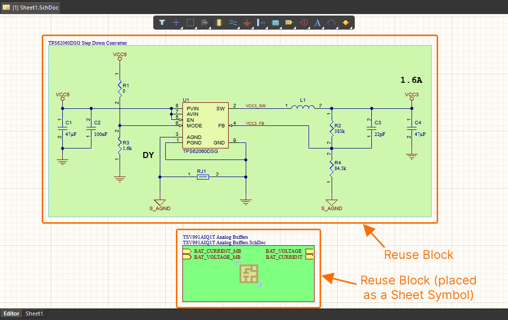
BusA bus is a polyline object that represents a multi-wire connection. Buses are used to bundle a series of sequential nets, for example, an address bus or a data bus. Their core requirement is that each net in the bus is named with a common base name, followed by a numeric identifier. In the example above, six individual nets (MB_ESC_M1 - MB_ESC_M6) arrive on the sheet having been bundled into the bus MB_ESC_M[1..6]. Learn more... Bus EntryA bus entry is an electrical design primitive that is used to connect a wire to a bus line. It has the ability to allow two different nets to connect to the same point on a bus. If this was done using wires, the two nets would create a short. In the example above, the incoming bus (MB_ESC_M[1..6]) is split into its constituent nets using bus entries. Learn more... PartA part (or component) within a library represents the physical device that is placed on the actual printed circuit board. On a schematic sheet, a component is represented by its schematic symbol model. Each component can contain one or more parts. Along with a symbolic representation of the component the part also includes links to models, such as the PCB footprint, and also parameters that are used to document details such as component parameters and supplier information. How the model links and parameters are added to the part depends on the type of library storage being used. Learn more... Part Designator & CommentThe Designator field is a child parameter object of a schematic component (part). It is used to uniquely identify each placed part to distinguish it from all other parts placed across the schematic source documents of the project. Learn more... The Comment field (also a child parameter object of a schematic component (part)) is used for displaying additional information for the component (such as part number or value). Learn more... Power PortA power port creates connectivity to every other power port of the same name throughout the schematic project, regardless of the design structure. The net is automatically named by the power port. This net can be localized to a specific schematic sheet if required. Learn more... WireA wire is a polyline electrical design primitive that is used to form electrical connections between points on a schematic. A wire is analogous to a physical wire. Learn more... Net LabelA net label is a net identifier used to create connectivity to other net labels with the same name on the same schematic sheet. The net is automatically named by the net label. Net labels can be placed on component pins, wires and buses. Note that net labels do not connect between sheets unless the project options are configured to use a Net Identifier Scope of Global. Learn more... PortA port is used to connect a net from one schematic sheet to another. Connectivity can be vertical (in a hierarchical design) or horizontal (in a flat design). Port names are used to name nets if the Allow Ports to Name Nets option is enabled on the Options tab of the Project Options dialog. In this situation, ports will also connect within the same schematic sheet. Learn more... Offsheet ConnectorAn offsheet connector is used to connect a net from one schematic sheet to another sheet (not within the same sheet). They only support horizontal connectivity (flat designs) and have limited functionality when compared to ports. Learn more... Sheet SymbolA sheet symbol is used to represent a sub-sheet in a multi-sheet hierarchical design. A hierarchical design is one where the structure – or sheet-to-sheet relationships – in the design is represented. The advantage of the hierarchical design is that it shows the structure of the design and that the connectivity is completely predictable and easily traced since it is always from the child sheet up to the sheet symbol on the parent sheet. Another advantage of a hierarchical design is that it provides the platform for the delivery of a sophisticated design reuse system. This system is delivered through either managed schematic sheets or device sheets, depending on whether the system is Workspace-based or file-based. In each case, the symbol placed differs in its coloring and includes a graphic to distinguish it as referencing a reusable entity, but the functionality and behavior are essentially that of the standard sheet symbol. Learn more... Sheet EntryA sheet entry is placed within a sheet symbol to create connectivity to a port of the same name on the source schematic sub-sheet that the symbol represents. Sheet entries are used as net names if the Allow Sheet Entries to Name Nets option is enabled in the Options tab of the Project Options dialog. Learn more... Sheet Symbol DesignatorThe sheet symbol designator, which is a child object of the parent sheet symbol, is used to provide the symbol with a meaningful name that will distinguish it from other sheet symbols placed on the same schematic sheet. Typically, the name will reflect the overall function of the schematic sub-sheet that the symbol represents. By using sheet symbol instantiation, multiple channels on the same sub-sheet can be referenced from a single sheet symbol. The syntax used involves the use of the Repeat keyword in the sheet symbol's Designator field. Learn more... Sheet Symbol File NameThe sheet symbol file name is a child object of the parent sheet symbol and provides the link between the sheet symbol and the schematic sub-sheet that the symbol represents. Multiple sub-sheets may be referenced by a single sheet symbol by separating each filename with a semi-colon in the File Name field. Learn more... Reuse BlockA reuse block allows you to save and reuse sections of design circuitry across different projects. It can contain both schematic circuitry and its physical representation for the PCB. When such a reuse block is placed on a schematic sheet, its physical representation will be placed automatically in the PCB document during the ECO process. Reuse blocks are formally-managed Workspace entities – these blocks are read-only, lifecycle-/revision-controlled (blocks can be updated) and traceable (where-used support). A reuse block can be placed on a schematic sheet directly or as a sheet symbol on the schematic sheet. In the latter case, the placed sheet symbol will include sheet entries corresponding to ports in the reuse block. The content of the reuse block will be placed on an automatically created child schematic sheet referenced by the sheet symbol. The sheet symbol of a placed reuse block will have a distinctive icon. Learn more... Signal HarnessA signal harness is an abstract connection that enables the logical grouping of different signals, including buses, wires, and other signal harnesses, for increased flexibility and streamlined design. Signal harnesses allow for the creation and manipulation of higher-level abstract connections between sub-circuits in PCB projects. They allow for a more complex design within the same schematic design space, which increases the readability of designs and builds potential for reuse. Learn more... Harness ConnectorA harness connector is essentially a container that groups various signals together to form a signal harness, including buses, wires, and other signal harnesses. Think of a harness connector as a funnel that gathers all of the signals that connect to this harness through the included harness entries. Learn more... Harness EntryA harness entry is placed within a harness connector and is the connection point through which signals – through wires, buses and other signal harnesses – are combined to form a higher-level signal harness. Learn more... Harness TypeThe harness type, which is a child object of the parent harness connector, is used to name the type of placed harness connector or the set of harness entries defined within it. The harness type and its associated harness entries are essentially the names of the containers that carry the nets, not the names of the nets themselves. Learn more... PinPins are placed in the Schematic Library editor to represent the physical pins on the component. Only one end of the pin is electrically active, which is sometimes referred to as the hot end of the pin. Learn more... ProbeA probe is used to take measurements at specific locations of a simulation-ready circuit. Probes can be used to interrogate the voltage, current or power at an applicable location, and even a voltage differential (using two sequentially-placed probes). You can also enable interactive mode for probes to immediately reflect any changes (adding/removing probes, enabling/disabling probes, moving a probe to a different location, changing probe color) in the No ERC DirectiveA no ERC design directive is placed on a node in the circuit to suppress all reported Electrical Rule Check warnings and/or error violation conditions that are detected when the schematic project is validated. Use no ERC to deliberately limit error checking at a certain point in the circuit that you know will generate a warning (such as an unconnected pin) while still performing a comprehensive check of the rest of the circuit. Learn more... Differential Pair DirectiveA differential pair directive (a predefined parameter set directive) allows you to define a differential pair object on the schematic. Attach a directive of this type to both the positive and negative nets of the intended pair or cover the pair with a blanket object to target multiple nets with a single directive. The nets themselves must be named with the suffixes of _P and _N. Custom differential pair suffixes can be defined in the Diff Pairs section on the Options tab of the Project Options dialog.
Each pair of directives (one for the positive net and one for the negative net) of this type will yield a differential pair object when transferred to the PCB during the synchronization process. Each of these differential pair objects will be added to the default differential pair class of All Differential Pairs. The name of a generated differential pair object will be the root name for the net pair on the schematic. For example, directives added to Parameter Set DirectiveA parameter set directive allows design specifications to be associated with a net-type object within a schematic design. For example, use a parameter set directive to define PCB layout constraints, differential pairs and net classes. It is the presence of specifically-named parameters in the parameter set directive that the software uses to determine which design directive you are placing. Learn more... Blanket DirectiveWhere a parameter set directive can only target the specific net that it is attached to, when combined with a Blanket directive, its scope can be expanded to cover all nets within the blanket. A blanket directive is placed over a collection of nets and/or components. You can either define a simple rectangular shape or a polygonal shape. The latter gives more precise control over the coverage of the required net objects on a sheet. A parameter set directive applied to the blanket will then apply to all nets and components that the blanket covers. Learn more... Compile Mask DirectiveNo ERC directives are great for suppressing a low number of violating pins, ports, sheet entries, or nets within a design. However, in some cases, it may be desirable to remove an entire section of the design, including components. Use a compile mask directive to effectively hide the area of the design it contains from the Compiler (when performing a manual validation), allowing you to manually prevent error checking for circuitry that may not yet be complete and will generate compile errors. This can prove very useful if you need to validate the active document or project to check the integrity of the design in other specific areas but do not want the 'noise' of compiler-generated messages associated with unfinished portions of the design. This feature can also be put to great use when simulation is included as part of the design flow, as in the example above. Voltage and current sources are necessary elements when running circuit simulations, but they have no place on the completed PCB. By applying a small amount of planning to the structure of the circuit, it is usually possible to group all simulation-specific components in one section of the design that can then be easily covered by a compile mask directive. Learn more... |


Schematic Document Commenting
A comment can be applied to an object, a specific point, or an area in a schematic document. A comment is a user-added note that may be replied to by other users. Comments promote collaboration between users without altering the shared data itself, because comments are stored by the connected Workspace independently of that data. Comments are posted, replied to, and managed directly within the design space using a contextual commenting window in conjunction with the Comments and Tasks panel.
For more information, refer to the Document Commenting page.
A-Z Listing
The following is a convenient alphabetical listing - no frills, no fuss - to be able to get at more detail for a particular design object in true QuickNav fashion.