
Capturing the Schematic
You are now ready to begin capturing (drawing) the schematic.
Placing the Components
Main page: Searching for & Placing Components
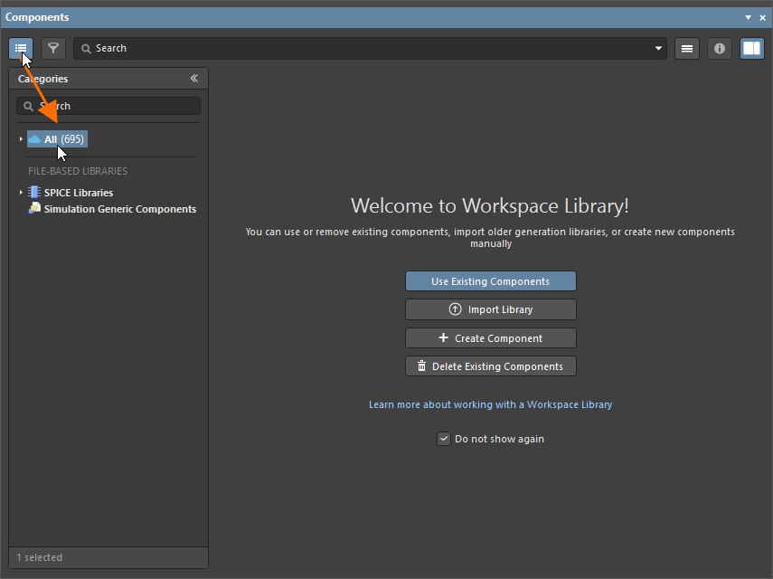
When Altium Designer is connected to a Workspace, the Components panel will list all components available for use in a project design, from this Workspace. For such components, the Components panel supports the same search features that are available in the Manufacturer Part Search panel, including string-based searching, faceted searching, or a combination of both, and also the Find Similar Components feature.
With the Components panel, components acquired from the Manufacturer Part Search panel will be placed in the multivibrator circuit. Once you have placed the components, the schematic should look like the image below.

All the components have been placed, ready for wiring.
Notes on Object Placement and Editing
-
While the object (such as a component) is floating on the cursor, you can:
-
Press
Spacebarto rotate it counterclockwise in 90º increments -
Press
Xto flip it along the X-axis -
Press
Yto flip it along the Y-axis.
-
-
To edit the properties of an object prior to placement, press
Tabto pause the editing process and display the Properties panel. The default behavior is for the most commonly edited field to be highlighted, ready for editing. Because the editing process is paused, you can use the cursor (or pressTabon the keyboard) to move to another field in the panel. The entered values become the defaults. For a component, the designator will be auto-incremented, if it has the same prefix. When you have finished editing, click the pause button in the design space ( ) to return to object placement (
 ).
).
-
While you can edit object properties during placement, you can leave the editing until after the object is placed. To do this, you can double-click the placed object to select it and open the Properties panel.
-
Multiple objects can also be selected. Use
Shift+Clickto sequentially select the objects or use a selection rectangle (Click, Hold&Dragaway from objects) to select all objects that fall within the bounds of the selection area. -
The Properties panel supports editing multiple selected objects at the same time.
-
If all objects share a property, that property will be available for editing.
-
If all objects share the same property value, that value will be displayed.
-
If objects share the same property but have different values, it will display an asterisk (*).
-
The value entered or the option chosen is applied to all selected objects.
-
-
During object placement, Altium Designer will automatically pan if you touch the edge of the design space. Autopanning is configured in the Schematic – Graphical Editing page of the Preferences dialog (accessed by clicking the
 button at the top left of the design space). If you accidentally pan beyond where you want, while the object is floating on the cursor, use
 Ctrl+Mouse WheelandRight-Click, Hold&Dragto zoom and pan orCtrl+PgDnto display the entire sheet again. -
To reposition any object, place the cursor directly over it, click and hold the left mouse button, drag the object to a new position then release the mouse button. Movement is constrained to the current snap grid, which is displayed on the Status Bar. Press the
Gshortcut at any time to cycle through the current snap grid settings. The grids you cycle through when you press theGshortcut are defined in the Schematic – Grids page of the Preferences dialog. It is recommended to position the components on a coarse grid, such as 50 or 100 mils, to keep the circuit neat and make it easy to attach wires to pins. For a simple design such as this tutorial's design, 100 mils is a good choice. -
You can also re-position a selected schematic object or a group of objects using the arrow keys on the keyboard. Select the objects then press an
arrow keywhile holding down theCtrlkey. HoldShiftas well to move objects by 10 times the current snap grid.
Learn more about Schematic Placement & Editing Techniques.
Placing the Transistors
-
Select View » Fit Document from the main menus to make the schematic sheet fill the design space.
-
Open the Components panel. To do this, click the
 button at the bottom right of the design space and select Components from the menu.
-
Click the
 button at the top left of the Components panel to open the Categories pane. Select the All entry to access the Workspace library.
After that, the Categories pane can be closed by clicking the
 button.
-
Click the
 button at the top of the Components panel and select Refresh from the menu to update the panel's content with the components acquired from the Manufacturer Part Search panel.

-
In the Search field at the top of the panel, type
transistor BC547. Search results will be presented in the panel.
-
Click the entry of the found transistor (BC547CG) in the search result grid to select it.
-
Display the Details pane of the panel using the
 button so that you can explore the details of the selected component.

-
Click the required transistor in the results grid of the panel to select it then click the
 button in the Details pane. The cursor will automatically move to be within the bounds of the schematic sheet and change to a crosshair, with a symbol of the transistor floating on it. You are now in component placement mode. If you move the cursor around, the transistor will move with it.
Do not place the transistor yet!

-
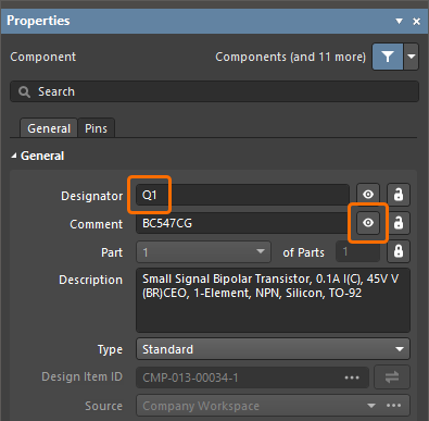
While the transistor is still floating on the cursor, press the
Tabkey to open the Properties panel. As the most-used field, the Designator field will be automatically highlighted in the panel, ready for editing.
-
Type
Q1in the Designator field and confirm that the visibility control for the Comment field is set to visible (shown as ).
).
-
Leave all other fields at their default values and click the pause button in the design space (
) to return to component placement.
-
Move the cursor, with the transistor symbol attached, to position the transistor a little to the left of the middle of the sheet. Once you are happy with the transistor's location, click to place it on the schematic.

-
Move the cursor and you will find that a copy of the transistor has been placed on the schematic sheet, and you are still in component placement mode with the transistor symbol floating on the cursor. This feature allows you to place multiple instances of the same component.
-
You are ready to place the second transistor. This transistor is the same as the previous one so there is no need to edit its attributes before you place it. Altium Designer will automatically increment the component designator when you place multiple instances of the same component. In this case, the next transistor will automatically be designated Q2.
If you refer to the schematic diagram shown above, you will notice that Q2 is drawn as a mirror of Q1. To horizontally flip the orientation of the transistor floating on the cursor, press the
Xkey on the keyboard. -
Move the cursor to position the component to the right of Q1.

-
Once you have positioned the component, click to place Q2. Once again, a copy of the transistor you are "holding" will be placed on the schematic, and the next transistor will be floating on the cursor ready to be placed.
-
Since both of the transistors have been placed, exit component placement by right-clicking or pressing the
Esckey. The cursor will revert back to a standard arrow.
Placing the Capacitors
-
Return to the Components panel and use the panel's Search field to search for
capacitor 22nF 16V 0603. -
Select the entry of the found capacitor (Capacitor 22nF +/-5% 16V 0603) in the search result grid.
-
Many of the resistors and capacitors have several footprint models, for different density levels. Under the footprint preview in the Models region of the Details pane, select the A variety (FP-C0603C-CF-IPC_A).

-
Click the
button in the Details pane.
-
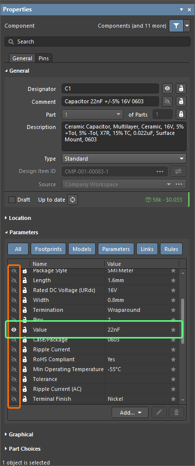
While the capacitor is floating on the cursor, press the
Tabkey to open the Properties panel. -
Type
C1in the Designator field. -
Click the Show More link in the panel's Parameters region to show the full list of component parameters. Make sure that the visibility of the Value parameter is only enabled. The value of this parameter will be shown next to the component in the design space.
-
Leave all other fields at their default values and click the pause button in the design space (
) to return to component placement.
-
Press
Spacebarto rotate the component in 90° increments until it has the correct orientation. -
Position the capacitor above the transistors and click to place the component.

-
Position and place capacitor C2.

-
Right-click or press
Escto exit the component placement.
Placing the Resistors
-
Return to the Components panel and use the panel's Search field to search for
resistor 100K 5% 0805. -
Select the entry of the found 100K resistor (Resistor 100K +/-5% 0805 125 mW) in the search result grid.
-
Under the footprint preview in the Models region of the Details pane, select the M variety (RESC2013X70X40ML20T20).
-
Click the
button in the Details pane.
-
While the resistor is floating on the cursor, press the
Tabkey to open the Properties panel. -
Type
R1in the Designator field. -
Click the Show More link in the panel's Parameters region and make sure that the visibility of the Value parameter is only enabled.
-
Leave all other fields at their default values and click the pause button in the design space (
) to return to component placement.
-
Press
Spacebarto rotate the component in 90° increments until it has the correct orientation. -
Position the resistor above and to the left of the base of Q1 and click to place the component.

-
Next, place the other 100K resistor, R2, above and to the right of the base of Q2. The designator will automatically increment when you place the second resistor.

-
Right-click or press
Escto exit the component placement. -
Return to the Components panel and use the panel's Search field to search for
resistor 1K 5% 0805 fixed. -
Select the entry of the found 1K resistor (Resistor 1K +/-5% 0805 500 mW) in the search result grid.
-
Under the footprint preview in the Models region of the Details pane, select the M variety (RESC2013X70X40ML20T20).
-
Click the
button in the Details pane.
-
While the resistor is floating on the cursor, press the
Tabkey to open the Properties panel. -
Type
R3in the Designator field. -
Click the Show More link in the panel's Parameters region and make sure that the visibility of the Value parameter is only enabled.
-
Leave all other fields at their default values and click the pause button in the design space (
) to return to component placement.
-
Press
Spacebarto rotate the component in 90° increments until it has the correct orientation. -
Position and place R3 directly above the collector of Q1, then place R4 directly above the collector or Q2.

-
Right-click or press
Escto exit the component placement.
Placing the Connector
-
Return to the Components panel and use the panel's Search field to search for
connector male straight. -
Select the entry of the found connector in the search result grid.
-
Click the
button in the Details pane.
-
While the resistor is floating on the cursor, press the
Tabkey to open the Properties panel. -
Type
P1in the Designator field. -
Leave all other fields at their default values and click the pause button in the design space (
) to return to component placement.
-
Press
Spacebarto rotate the component in 90° increments until it has the correct orientation. -
Click to place the connector on the schematic.

-
Right-click or press
Escto exit the component placement. -
Save the schematic document locally by right-clicking its entry in the Projects panel and selecting Save from the context menu.
Wiring the Circuit
Main page: Creating Circuit Connectivity in Your Schematics
Wiring is the process of creating connectivity between the various components of your circuit. To wire up your schematic, refer to the sketch of the circuit ( ) and the video shown below.
Notes on Wiring
-
To start wiring, select the Place » Wire command from the main menus (shortcut:
Ctrl+W). -
Click to anchor the wire at the cursor position.
-
Press
Backspaceto remove the last anchor point. -
Press
Spacebarto toggle the direction of the corner. You can observe this in the video shown above toward the end when the connector is being wired. -
Right-click or press
Escto exit wire placement mode. -
Click, Hold&Dragto drag the component together with any connected wires.Ctrl+Click, Hold&Dragto move a placed component. -
Whenever a wire crosses the connection point of a component or is terminated on another wire, a junction will automatically be created.
-
A wire that crosses the end of a pin will connect to that pin.
Use the wiring tool to wire up your circuit. Toward the end of the video, you can see how wires can be dragged.
-
First, wire the lower pin of resistor R1 to the base of transistor Q1 in the following manner. Select the Place » Wire command from the main menus (or use the
Ctrl+Wshortcut) to enter the wire placement mode. The cursor will change to a crosshair. -
Position the cursor over the bottom end of R1. When you are in the right position, a red connection marker (red cross) will appear at the cursor location. This indicates that the cursor is over a valid electrical connection point on the component.
-
Click to anchor the first wire point. Move the cursor, and a wire will extend from the cursor position back to the anchor point.
-
Position the cursor over the base of Q1 until you see the cursor change to a red connection marker. If the wire is forming a corner in the wrong direction, press
Spacebarto toggle the corner direction. -
Click to connect the wire to the base of Q1. The cursor will release from that wire.
-
Note that the cursor remains a crosshair indicating that you are ready to place another wire. To exit placement mode completely and go back to the arrow cursor, you would right-click or press
Esc– but do not do this just now. -
Next, wire from the lower pin of R3 to the collector of Q1. Position the cursor over the lower pin of R3 and click to start a new wire. Move the cursor vertically until it is over the collector of Q1, then click to place the wire segment. Again, the cursor will release from that wire and you remain in wiring mode, ready to place another wire.
-
Wire up the rest of your circuit, as shown in the video above.
-
When you have finished placing all the wires, right-click or press
Escto exit placement mode. The cursor will revert to an arrow.
Placing the Net Labels
Each set of component pins that you have connected to each other now forms what is referred to as a net. For example, one net includes the base of Q1, one pin of R1, and one pin of C1. Each net is automatically assigned a system-generated name, which is based on one of the component pins in that net.
To make it easy to identify important nets in the design, you can add net labels to assign names. For the multivibrator circuit, you will label the 12V and GND nets in the circuit, as shown below.

Net labels have been added to the 12V and GND nets, completing the schematic.
-
Select the Place » Net Label command from the main menus. A net label will appear floating on the cursor.
-
To edit the net label before it is placed, press
Tabto open the Properties panel. -
Type
12Vin the Net Name field.
-
Click the pause button in the design space (
) to return to object placement.
-
Place the net label so that its hotspot (the bottom-left corner) touches the uppermost wire on the schematic, as shown in the images below. The cursor will change to a red cross when the net label is correctly positioned to connect to the wire. If the cross is light gray, it means there will not be a valid connection made.
 and positioned over a wire (the bottom image), note the red cross.")
The net label in free space (the top image) and positioned over a wire (the bottom image), note the red cross. -
After placing the first net label, you will still be in net label placement mode. Press the
Tabkey again to edit the second net label in the Properties panel before placing it. -
Type
GNDin the Net Name field. -
Click the pause button in the design space (
) to return to object placement.
-
Place the net label so that the bottom left of the net label touches the lowermost wire on the schematic (as shown in the completed schematic image above). Right-click or press
Escto exit net label placement mode. -
Save the schematic document locally by right-clicking its entry in the Projects panel and selecting Save from the context menu.
Congratulations! You have just completed your first schematic capture. Before you turn the schematic into a circuit board, you need to configure the project options and check the design for errors.
Configuring Project Options
Main page: Accessing, Defining & Managing Project Options
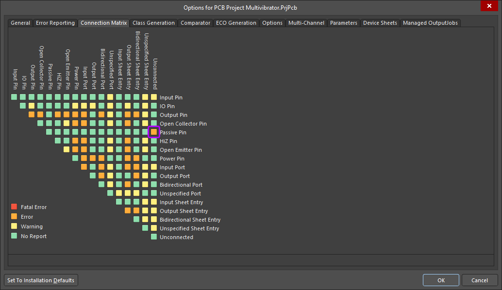
Project-specific settings are configured in the Project Options dialog. The project options include error reporting settings, a connectivity matrix, class generation settings, and more. Some project options are shown and described below.
|
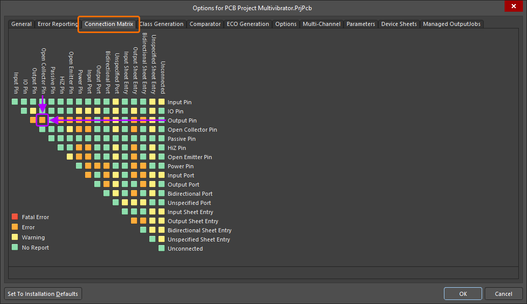
When you validate a project, Altium Designer checks for logical, electrical, and drafting errors between the schematic content and error reporting settings. The Error Reporting tab of the Project Options dialog is used to set up a wide range of checks. The Report Mode settings show the level of severity of a violation. If you want to change a setting, click on current Report Mode next to the violation you want to change and choose the level of severity from the drop-down list. As the design is coming along, a list of the pins in each net is built into memory. The type of each pin is detected (e.g., input, output, passive, etc.), then each net is checked to see if there are pin types that should not be connected to each other, for example, an output pin connected to another output pin. The Connection Matrix tab of the Project Options dialog is where you configure what pin types are allowed to connect to each other. For example, look at the entries on the right side of the matrix diagram and find Output Pin. Read across this row of the matrix until you get to the Open Collector Pin column. The square where they intersect is orange, indicating that an Output Pin connected to an Open Collector Pin on your schematic will generate an error condition when the project is validated. You can set each error type with a separate error level, i.e., from No Report to a Fatal Error. Click on a colored square to change the setting; it will cycle through the four possible settings. The Class Generation tab of the Project Options dialog is used to configure what type of classes are generated from the design (the Comparator and ECO Generation tabs are then used to control if classes are transferred to the PCB). The Comparator tab of the Project Options dialog sets which differences will be reported or ignored when comparing documents. When you need detailed control, you can selectively configure the comparator using the individual comparison settings. |


-
Right-click the project entry in the Projects panel and select the Project Options command from the context menu to open the Project Options dialog, then select the Error Reporting tab of the dialog.

-
Scroll through the list of error checks and note that they are clustered in groups. Each group can be collapsed if required.
-
Click on the Report Mode setting for any check and note the options available.
-
Select the Connection Matrix tab of the Project Options dialog.
-
Your circuit contains only passive pins. Look down the row labels to find the Passive Pin row. Look across the column labels to find Unconnected. The square where these entries intersect indicates the error condition when a passive pin is found to be unconnected in the schematic. The default setting is green (
 ) indicating that no report will be generated.

-
Change the default settings so that the connection matrix detects unconnected passive pins. Click on this intersection box until it turns orange (
 ) so that an error will be generated for unconnected passive pins when the project is validated. You will purposely create an instance of this violation later in the tutorial.
-
Select the Class Generation tab of the Project Options dialog.
-
For a simple, single-sheet design such as this, there is no need to generate a component class. Clear the Component Classes checkbox for the project's schematic document.

-
Click OK to apply changes and close the Project Options dialog.
-
Save the project locally by right-clicking its entry in the Projects panel and selecting Save from the context menu.
You are now ready to validate the project and check for any errors.
Validating the Project
Main page: Validating Your Design Project
Validation of a project checks for drafting and electrical rules errors in the design documents, and details all warnings and errors in the Messages panel. You have set up the check settings in the Error Checking and Connection Matrix tabs of the Project Options dialog, so you are now ready to check the design.
-
To validate the Multivibrator project, right-click its entry in the Projects panel and select Validate PCB Project Multivibrator.PrjPcb from the context menu.

-
All validation warnings and errors are displayed in the Messages panel. The panel will only open automatically if there are errors detected (not when there are only warnings). To open it manually, click the
button at the bottom right of the design space and select Messages from the menu.
-
If your circuit is drawn correctly, the Messages panel should not contain any errors, only the message
Compile successful, no errors found. If there are errors, work through each one, checking your circuit, and ensuring that all wiring and connections are correct.
You will now deliberately introduce an error into the circuit and validate the project again.
-
Click in the middle of the wire that connects P1 to the emitters of Q1 and Q2 (the wire of net GND). Small, square editing handles will appear at each vertex of the wire and the selected color will display as a dotted line along the wire to indicate that it is selected. Press the
Deletekey to delete the wire.
-
Validate the project again (select Validate PCB Project Multivibrator.PrjPcb from the right-click menu of the project entry in the Projects panel). The Messages panel will display error messages indicating you have unconnected pins in your circuit.

Before you finish this section of the tutorial, fix violations in the schematic.
-
Undo the delete action (
Ctrl+Z) to restore the deleted wire. -
Validate the project again to check that there are no longer any violations. The Messages panel should show no violations.
-
Save the project to the Workspace. To do this, click the Save to Server control next to the project entry in the Projects panel, enter a meaningful comment into the Comment field of the Save to Server dialog that opens (e.g.,
Schematic is created and validated), and then click the OK button.
Configuring the Bill of Materials
Main page: BOM Management with ActiveBOM
Ultimately, every component used in a design must have detailed supply chain information. Rather than requiring that this information be added to each design component or added as a post-process in an Excel spreadsheet, you can add it at any point through the design cycle in an ActiveBOM document (*.BomDoc).
-
Right-click on the project entry in the Projects panel then select the Add New to Project » ActiveBOM command from the context menu. A new ActiveBOM document will open and an entry for it will appear linked to the project in the Projects panel under the Source Documents entry.
-
Right-click the ActiveBOM document entry in the Projects panel and select the Save As command. The Save As dialog will open, ready to save the document in the same location as the project file. Type the name
Multivibratorin the File name field and click the Save button. -
Adding the ActiveBOM document has changed the project, so save the project locally by right-clicking the project entry in the Projects panel and selecting Save.
-
The components used in the design will be listed as BOM items. By default, there is a column titled Line #. Click the
 button at the top of the document to populate this column.

-
Note that the BOM items grid includes a BOM status column on the right. Hover the mouse cursor over a status icon for information about any issues detected. The status icons should indicate that all of the BOM items include the violation No MPN ranked. This means that you have not yet checked through the selected manufacturer part numbers (MPNs) and indicated that you are happy with each of them.

It is possible that the transistor may have other errors. This will be resolved shortly.
-
Assign a 5-star rank to the MPN of each item that shows no violation type other than No MPN ranked (i.e., all items except for the transistor). To do this, click on a BOM item in the grid and then click the rightmost star in the lower region of the document that displays the supply chain information for this item. After that, the status of four of the five BOM items should change to green indicating that these items are clear (ready to order).
-
Select the transistor item. It may have the manufacturing lifecycle Obsolete. For this item, we will add another MPN by adding a part choice to the component in the Workspace library. To do this, click the
 button and select Edit Part Choices in Library from the drop-down menu.

-
The Edit Part Choices dialog will open. Click the
 button to open the Add Part Choices dialog. This dialog is used to search for a suitable manufacturer part in the same way as the Manufacturer Part Search panel.

-
In the Search field at the top of the Add Part Choices dialog, type
BC547Cand pressEnterto broaden the search.
-
Keep an eye on the vertical colored bar at the edge of the Manufacturer Part column. This indicates the lifecycle state of that part. Ideally, you will select a part with a green lifecycle state (Volume Production). Hover the cursor over the vertical colored bar to view the lifecycle state. Note that you do not need the part to have models since you already have a symbol on the schematic and a footprint on the PCB.
Choose a part with a suitable lifecycle state and stock available (e.g., BC547CTFR from ON Semiconductor / Fairchild), then click OK to accept this part.

-
You will return to the Edit Part Choices dialog, where the selected part will be listed.

Click OK to close the dialog and return to the ActiveBOM document.
-
The lower region of the document will show two MPNs for the transistor: one derived from the original part choice added during the component creation and another derived from the part choice you just added. Use the ranking feature to promote the part you selected to be the primary solution for this BOM item.

-
All BOM items now include proper supply chain details. Save the ActiveBOM document locally by right-clicking its entry in the Projects panel and selecting Save from the context menu.
-
Save the project to the Workspace. To do this, click the Save to Server control next to the project entry in the Projects panel, enter a meaningful comment into the Comment field of the Save to Server dialog that opens (e.g.,
BOM document added), and then click the OK button. -
Close the ActiveBOM document by right-clicking its tab at the top of the design space and selecting the Close Multivibrator.BomDoc command from the context menu.


