トラックの操作
トラックセグメントは、定義された幅の直線です。PCB設計空間で直線を定義するためにトラックを使用します。トラックは信号層上に配置され、コンポーネントパッド間の電気的な接続、または配線を形成します。非電気層上に配置されたトラックはラインと呼ばれ、コンポーネントのアウトライン、指示情報、禁止領域境界などを作成するための汎用描画要素として使用されます。トラックは、寸法や座標などのグループ設計オブジェクトにも使用されます。
トラックオブジェクトは、配線や一般的な線の描画に使用されます。上の画像には4つの配置されたトラックセグメントがあり、もう1つが配置中です。
トラックとラインは実際には同じオブジェクトですが、配置中のソフトウェアの振る舞いが異なるため、異なるコマンドが存在します。たとえばインタラクティブ配線のようなトラック配置コマンドを実行すると、ソフトウェアはクリック位置を監視し、クリック位置の下にある既存のオブジェクト(パッドなど)のネット名を自動的に採用します。また、適用可能な設計ルールも監視し、従います。一方、ライン配置コマンド(Place » Line)を実行すると、これらの監視動作は行われません。
トラックは、PCBエディタとPCBライブラリエディタの両方で配置できます。コマンド(配線/トラックまたはライン配置)に関係なく、基本的な配置動作は同じです。コマンドを起動すると、カーソルが十字線に変わり、トラック配置モードに入ります。配置は、次の一連のアクションを実行することで行われます:
-
最初のトラックセグメントの開始点を固定するために、Enterキーを押すかクリックします。配線タイプの配置コマンドを実行していて、既存のオブジェクト上で配置を開始するためにクリクした場合、トラックはそのオブジェクトのネット名を採用します。配線の場合、幅は適用される配線幅設計ルールによって決定されます。これは、以下で詳しく説明されている特定のインタラクティブ配線オプションによって上書きされることがあります。
-
カーソルを移動してトラックセグメントを定義し、そのセグメントの終点(次に接続されるセグメントの開始点でもある)を固定するためにEnterキーを押すかクリックします。
-
カーソルを位置に合わせてから、接続されたトラックセグメントの一連を定義する頂点ポイントのシリーズを固定するためにEnterキーを押すかクリックし続けます。
-
現在の接続されたトラックセグメントのシリーズを終了するために、右クリックまたはEscキーを押します。
配置中に実行できる追加のアクションには以下が含まれます:
-
数値キーパッドの*キーを押して、利用可能な信号層を順に切り替えます。または、Shift+Ctrl+ホイールロールの組み合わせを使用して、配線層を移動します。マウスホイールの各ノッチが次の(または前の)利用可能な信号層に移動します。
-
数値キーパッドの+キーと-キーを押して、設計で現在表示されているすべての層を前後に順に切り替えます。
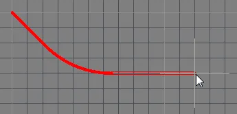
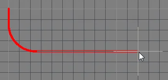
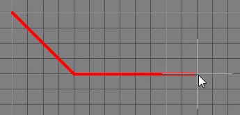
トラックセグメントを配置する際には、5つの利用可能なコーナーモードがあり、そのうち4つにはコーナー方向のサブモードもあります。配置中に:
-
Shift+Spacebarを押して、利用可能なコーナーモードを切り替えます。
-
Spacebarを押して、2つのコーナー方向サブモード間で切り替えます。
-
アークコーナーモードのいずれかにいる場合、,キーまたは.キーを押し続けることでアークを縮小または拡大します。アークのサイズ変更を加速するには、押すときにShiftキーを押し続けます。
-
1のショートカットキーを押して、クリックごとに1セグメントを配置する(下の最初の5枚の画像に示されている)か、2セグメントを配置する(下の最後の画像に示されている)かを切り替えます。最初のモードでは、中空のトラックセグメントを先読みセグメントと呼びます。
-
Backspaceキーを押して、最後の頂点を削除します。


5つの利用可能なコーナーモードを切り替えるにはShift+Spacebarを押し、コーナーの方向を切り替えるにはSpacebarを押し、1セグメントと2セグメントの配置を切り替えるにはショートカット1を押します。 グラフィカルな編集方法を使用すると、配置されたトラックオブジェクトを設計空間内で直接選択し、そのサイズ、形状、または位置をグラフィカルに変更できます。 トラックオブジェクトが選択されると、次の編集ハンドルが利用可能になります:
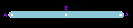
選択されたトラック
-
Aをクリックしてドラッグして、トラックの端点を再配置します。
-
Bをクリックしてドラッグして、トラックの形状を変更します。
PCBエディターには、配線の配置を維持できるようにボード上のトラックセグメントを移動するための高度なアルゴリズムが含まれています。このトラックセグメントのスライドは、特別なカーソルが表示されたときにトラックセグメントを最初に選択してクリックし、その後クリックして保持してセグメントをスライドさせるか、またはトラックセグメントをクリックして保持してスライドさせることによって、対話的に呼び出すことができます。スライド動作は、PreferencesダイアログのPCB Editor - Interactive RoutingページのDraggingオプションを使用して設定できます。これらのオプションを使用すると、個々のトラックセグメントを自由に移動できるようにする場合に、トラックに移動アクションを割り当てることができます。

設定のレベルでドラッグオプションを設定することにより、トラックスライディングの挙動を制御します。
これらのオプションを通じてMoveアクションが割り当てられている場合、移動中にトラックセグメントを回転させたり、ミラー化したりすることができます。
インタラクティブ配線と適用可能な設計ルール
インタラクティブ配線中、デフォルトの動作では、ソフトウェアが適用可能な電気および配線設計ルールに従ってトラックセグメントが配置されるようにします。つまり、異なるネットに属する既存のトラックセグメントに違反する新しいトラックセグメントを配置することをソフトウェアは許可せず、代わりに設計ルールを満たすようにトラックセグメントをクリップします。このインタラクティブ配線の動作はRouting Conflict Resolutionモードとして知られています。デフォルトモードはStop at First Obstacleです(現在のモードはステータスバーに表示されます)。利用可能なモードを切り替えるには、Shift+Rを押します。
適用可能な設計ルールという用語は、配置されているオブジェクトに適用されるすべてのルールを意味します。設計ルールエンジンは、各ルールが適用されるオブジェクトを正確にスコープするシステムで動作します。配置中、現在の配置状況で適用される最優先ルールを決定するために設計ルールエンジンが照会されます。インタラクティブ配線中に適用されるルールには以下が含まれます:
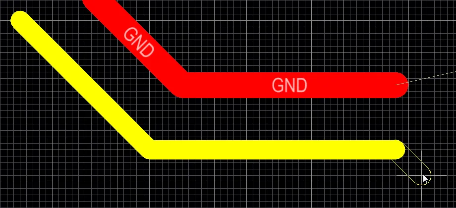
下のアニメーションは、配線の実行を示しています。GNDネットが定義された適用可能な配線幅設計ルールに従って配線されています。カーソルを+12Vネットに関連付けられたビアの上に移動すると、適用可能な電気クリアランス制約設計ルールが満たされるように、自動的にルートがクリップされていることに注意してください。

インタラクティブ配線中に適用される配線幅とクリアランスの設計ルールが自動的に守られます。
配線幅がどのように決定されるか
ルールエンジンが無効になっていない限り、ソフトウェアの上書き動作は常に、適用可能な配線幅設計ルールによって許可される範囲内で配線幅を保証することです。一般的なアプローチは、ネットの現在の運搬要件を満たしながらルートを適合させるための柔軟性を提供するために、ネットに使用される幅の範囲を許可することです。これをサポートするために、PCB Rules and Constraintsエディタには、幅の範囲を許可するために設定できるMin、Preferred、およびMaxの設定があり、特定の幅を要求するために同じに設定することもできます。幅はインピーダンスとしても設定でき、各信号層に対して異なる範囲が指定されることもあります。

新しいPCBのすべてのネットに適用されるデフォルトの配線幅設計ルール。
設計者として、配線を開始する際に最も適切な配線幅を選択するのに役立ついくつかのオプションがあります。これらは、以下に示すように、PreferencesダイアログのPCB Editor — Interactive Routingページで設定されます。

配線を開始するときに使用されるサイズを決定するInteractive Routing Width Sourcesオプション。
画像でTrack Width ModeがRule Preferredに設定されていることに注意してください。これは、パッドなどの既存のネットオブジェクト上でルートが開始される場合、この幅が使用されることを示しています。しかし、ルートが既存のトラック上で開始される場合は、Pickup Track Width From Existing RoutesオプションがTrack Width Modeを上書きし、新しい幅を既存の幅に合わせて設定します。
設計者として、配線中にShift+Wのショートカットを押して、異なる幅を選択できるダイアログにアクセスすることもできますし、Tabを押してプロパティパネルを開き、新しい幅の値を入力することもできます。選択または入力された値は、適用されるルールで定義されたMinとMaxの設定の間になければなりません。そうでない場合、自動的にこれらの最も近い値にクリップバックされます。
インタラクティブ配線のショートカット
配線中には、多くのショートカットを利用できます。例えば、Shift+R を押して利用可能な衝突解決モードを切り替えたり、Backspace を押して最後に配置した頂点(コーナー)を削除することができます。配線中にショートカットのリストを表示するには、Shift+F1 を押します。利用可能なインタラクティブショートカットのメニューが表示されます。必要なショートカットを選択するか、メニューを閉じてショートカットキーのシーケンスを使用するには Esc を押します。

インタラクティブ配線中に、利用可能なインタラクティブショートカットのメニューを表示するには、Shift+F1を押します
トラックの移動
Edit » Moveサブメニューとアクティブバーの移動コマンドメニューには、トラックの位置や形状を変更するために使用できる多数のコマンドが含まれています。

再配線
このコマンドを使用すると、ボード上の既存のトラックを手動で再配線できます。コマンドを起動すると、カーソルが十字線に変わり、トラックを選択するように求められます。必要なトラックの上にカーソルを合わせてクリックするか、Enterを押します。この機能の動作は、PreferencesダイアログのPCB Editor - Interactive RoutingページでPreserve Angle When Draggingオプションが有効になっているかどうかに依存します:
-
角度を保持してドラッグする機能が有効 - トラックが分断され、直交/対角接続を維持するために新しいセグメントが追加されます。必要に応じてこのセグメントをスライドさせてからクリックして配置します。この時点で右クリックまたはEscキーを押さないと、新しいセグメントがさらに分断されて別のセグメントが作成されます。Shift+R キーボードショートカットを使用して、ドラッグ中に障害物をどのように扱うかを制御するオプションを切り替えます(Ignore Obstacles、Avoid Obstacles、またはAvoid Obstacles (Snap Grid))。障害物を避けるモードのいずれかが有効になっている場合、ドラッグ中にルールが遵守され、セグメントを違反に導くドラッグが防止されます。
-
角度を保持してドラッグする機能が無効 - トラックセグメントの両端が固定され、2つの間に新しいトラックセグメントを敷設できるようになります。新しいトラックセグメントを配置するにはクリックまたはEnterキーを押します。リルートのために新しいトラックセグメントの配置を続けるか、右クリックまたはEscキーを押して停止します。
さらにトラックの再配線を続けるか、右クリックまたはEscキーを押して終了します。
-
角度を保持しながらドラッグする機能が有効になっている場合、ターゲットのトラックセグメントをクリックする前にAltキーを押し続けることで、一時的にこの機能を無効にすることができます。リルートする際には、Altキーを押し続けながら進めてクリックしてください。
-
このコマンドを使用してトラックをリルートする際、角度を保持しながらドラッグする機能を無効にしている場合、選択したトラックセグメントの左端からリルートを開始し、右端に向かって作業することをお勧めします。
-
類似のリルート機能は、トラックセグメントを選択してから、その中心頂点をクリックアンドドラッグすることで実現できます。その後、元のトラックに沿って一端から他端まで、結果として生じたセグメントの中心頂点を順にクリックアンドドラッグします。
トラックの分割
このコマンドを使用すると、トラックセグメントに頂点(または分割)を作成できます。コマンドを起動すると、カーソルが十字線に変わり、トラックの選択を促されます。分割を挿入したい特定のポイントで必要なトラックセグメント上にカーソルを位置づけ、クリックするかEnterを押します。頂点が挿入され、元のセグメントが二つに分割されます。
必要な位置に頂点を移動してから、クリックするかEnterを押して配置します。添付されたトラックセグメントは、PreferencesダイアログのPCB Editor - Interactive RoutingページにあるPreserve Angle When Draggingオプションの設定に従って動作します:
さらにトラックセグメントを分割するか、右クリックまたはEscキーを押して終了します。
Shift+Ctrl+クリック&ホールドのキーボードショートカットを使用して、現在のカーソル位置でトラックセグメントを分割することもできます。
トラックエンドのドラッグ
このコマンドを使用すると、配線されたトラックセグメントの端を手動で再配置またはドラッグすることができます。コマンドを起動すると、カーソルが十字線に変わり、オブジェクトの選択を促されます。カーソルをトラック上に置いてクリックするか、Enterを押します。すると、カーソルは最も近いトラックセグメントの端にジャンプし、トラックの端がカーソルにアタッチされます。トラックの端を希望の位置に移動してから、クリックするかEnterを押して配置を実行します。
-
選択したトラックセグメントの端が、他のトラックセグメントに接続されていない頂点である場合、その頂点を必要な位置に移動します。
-
選択したトラックセグメントの端が、2つのトラックセグメントに接続されている頂点である場合、頂点を移動すると接続されたトラックセグメントがゴムバンドのように伸びます。
-
トラックセグメントの端がコンポーネントのパッドに接続されている場合、端を移動するとパッドから切り離されます。端を再配置した後、Smart Track EndsオプションがPreferencesダイアログのPCB Editor – Generalページで有効になっている場合、トラックの端からパッドへの論理的な接続線が表示されます。
-
トラックセグメントの端がフリーパッドに接続されている場合、パッドがカーソルに付着し、再配置の準備ができます。パッドに接続された全てのトラックがゴムバンドのように伸びます。
-
トラックセグメントの端がビアに接続されている場合、ビアがカーソルに付着し、再配置の準備ができます。ビアに接続された全てのトラックがゴムバンドのように伸びます。
さらにトラックの端をドラッグし続けるか、右クリックまたはEscキーを押して終了します。
トラックの移動 / サイズ変更
このコマンドは、複数選択されたトラックセグメントの端点を移動し、セグメントのサイズを変更するために使用されます。コマンドを起動すると、カーソルが十字線に変わり、トラックの端点を選択するように求められます。トラックを移動/サイズ変更するには:
-
選択したセグメントの端点にカーソルを合わせてから、クリックまたはEnterキーを押します。
-
カーソルを動かすと、選択したトラックセグメントが動的にサイズ変更され、各セグメント間の元の距離と角度が維持されます。各セグメントの他端は、既存の接続/位置を維持するためにゴムバンドのように動作します。
-
セグメントが望む位置にある場合、クリックまたはEnterキーを押して配置を確定し、移動モードを終了します。
-
操作をキャンセルするには、右クリックまたはEscキーを押します。
セグメントを動かしている間、以下の追加コントロールが利用可能です:
-
Tabキーを押して、選択した各トラックセグメントの端点間でカーソルをサイクルします。
-
特定の方向に移動を制限するには、移動中にAltキーを押し続けます。可能な方向は、水平、垂直、および45度の角度です。
-
Spacebarを2回押して、トラックセグメントのすべての端点を水平または垂直面で一直線に素早く揃えます。再度Spacebarを素早く2回押すと、以前のサイズに戻ります。
このコマンドは、選択されていない単一のトラックセグメントの端点を移動するためにも使用できます。この場合、追加の制御としてAltキーのみが使用できることに注意してください。
トラックのスライス
トラックスライサーツールは、1つまたは複数のトラックセグメントを2つに切断するための簡単なメカニズムを提供し、現在の信号層またはすべての表示されている信号層のトラックをスライスすることができます。このツールにアクセスするには、メインメニューからEdit » Slice Tracksコマンドを選択します。
コマンドを起動すると、カーソルが十字線に変わり、スライスの開始位置を選択するように求められます。さらに、ワークスペース内のトラックオブジェクトのみが表示されるようにフィルタリングが適用されます。これは、トラックスライサーのアクティブな設定に応じて、すべての表示されている信号層のすべてのトラック、または現在の信号層のトラックのみになります。1つまたは複数のトラックをスライスするには:
-
カーソルを位置づけてから、クリックまたはEnterキーを押して、スライスの開始点を固定します。
-
スライスしたいトラックのポイント、またはトラック上をカーソルを移動させます - スライサーの経路は線で示され、予定されているカットが視覚的に描写されます。
-
クリックまたはEnterキーを押して、スライサーのトラックの終点を固定します。
-
さらにトラックセグメントをスライスするか、右クリックまたはEscキーを押してスライスモードを終了します。
スライスの初期アンカーポイントが選択された後、そして「スライスライン」を移動している間に実行できる追加のアクションは以下の通りです:
-
Bキーを押して、現在の信号層のみにトラックを切断するか、またはすべての可視信号層にわたってトラックを切断するかを切り替えます。
-
Spacebarを押して、切断角度を45度の増分または任意の角度に切り替えます。
-
Nキーを押して、スライサーブレードの側面を左、右、中央の間で切り替えます。
-
/キーを押して、すべての切断されたトラックを選択します。
-
","キーを押して、スライサーの左側にある切断されたトラックを選択します。
-
"."キーを押して、スライサーの右側にある切断されたトラックを選択します。
-
Mキーを押して、切断されたトラックを選択しないようにします。
-
Tabキーを押して、Slicer Propertiesダイアログにアクセスし、そこからトラックスライサーのプロパティをその場で変更できます。

Slicer Propertiesダイアログ
-
トラックセグメントは、ブレードが通過する範囲が結果として得られる2つのセグメント端のホットスポットの中心になるように切断されます。
-
スライサープロパティダイアログを通じて、スライシングブレードの幅を自由に定義できます。または、現在のスナップグリッドに基づいてブレードの幅を制約することもできます。Blade Widthの値がスナップグリッドの倍数でない場合、グリッド上になるように切り捨てられます。その結果の幅はグリッド幅として知られています。このオプションが無効かつBlade Widthが現在のスナップグリッドの倍数でない場合、結果として得られるトラックセグメント端の一方または両方がグリッド外になる可能性があります。Blade SideがLeftまたはRightに設定されている場合、ブレードの範囲の端にあるトラック端がグリッド外に位置します(開始位置軸に沿ったトラック端はグリッド上に残ります)。Blade SideがBothに設定されている場合、両方のトラック端がグリッド外になります。
-
Blade Sideオプションは、スライスの開始位置として選択された場所から決定された軸に関連して、スライスがどのように行われるかを制御します。設計空間では、選択された開始位置によって決定された軸が実線として表示され、ブレードの範囲が点線として表示されます。以下のオプションが利用可能です:
-
Left - スライスは開始位置軸の左側で行われます。スライス距離は、適用される場合、Blade Widthまたはグリッド幅の全幅に等しくなります。
-
Right - スライスは開始位置軸の右側で行われます。スライス距離は、適用される場合、Blade Widthまたはグリッド幅の全幅に等しくなります。
-
Both - スライスは開始位置軸の左右に等しく行われます。各側のスライス距離は、適用される場合、Blade Widthまたはグリッド幅の半分に等しくなります。
-
Cut Current Layer Onlyオプションを有効にすると、現在のレイヤー上のトラックセグメントのみをスライスします。このオプションを無効にすると、トラックスライサーの「パス」内にあるすべての可視レイヤー上のトラックセグメントをスライスします。
-
フィルタリングがワークスペースに適用されたときのマスキングの範囲は、View ConfigurationパネルのView OptionsタブのMask and Dim SettingsセクションにあるDimmed Objectsスライダーバーを使用して手動で調整できます。Shift+Cキーボードショートカットを使用してフィルタリングをクリアします。
トラックを面取りパスに変換する
マイクロ波周波数のルートにおけるコーナーによって引き起こされる反射を減少させる技術として、90度の配線コーナーの面取りが使用されます。弧を使用することもできますが、少なくともルート幅の3倍の半径が必要です。面取り(ミタリングとも呼ばれる)は、コーナーの外側の点を切り取る代替方法です。Altium Designerのトラックオブジェクトは丸みを帯びた端を持っているため、面取りコーナーを作成するためには使用できません。面取りコーナーを作成するためには、選択されたトラックセグメントをリージョンオブジェクトに置き換えます。
面取りするトラックセグメントを全て選択し、メインメニューからTools » Convert » Convert Selected Tracks to Chamfered Pathコマンドを選択します。Convert Tracks to Chamfered Pathダイアログが開きます。このダイアログを使用して面取りを設定し、OKをクリックします。選択された各トラックセグメントペア(問題のある90度の角度を持つ)は面取りされたコーナリングに置き換えられ、各ペアリング内の元のトラックセグメントは単一の固体(銅)領域オブジェクトに変換されます。

指定された量で、直角の角を持つ選択されたトラックが面取りされます。
ダイアログの以下のオプションを使用して、面取りを設定します:
面取りはどれくらいの大きさが適切か?
パーセンテージマイターは、マイター加工されていない曲げの内側と外側のコーナーの間の対角線の切り取られる部分の割合です。

DouvilleとJamesによって、幅広いマイクロストリップ構造における最適なマイターが実験的に決定されました。彼らは、最適なマイターの割合を示すのに適した式が以下のように与えられることを見出しました。

 および基板の誘電率定数
 が条件です。
この式は、完全に とは独立しています。DouvilleとJamesが証拠を提示するパラメータの実際の範囲は、
 および
および です。彼らは、式によって与えられたものの4%以内(元の
 の4%)の任意のパーセンテージマイターに対して、VSWRが1.1より良い(つまり、リターンが−26 dBより良い)ことを報告しています。最小の
 が0.25の場合、パーセンテージマイターは98.4%で、ストリップはほぼ完全に切断されています。
面取り処理は、複数のトラックセグメントを単一の領域オブジェクトに変換します。これは一方通行のプロセスであり、トラックが領域に変換されると、元に戻すことはできません。そのため、面取りはすべての配線が完了した後にのみ実行するべきです。不確かな場合は、面取りを行う前にボードのコピーを保存しておくことをお勧めします。
トラックのプロパティ

PropertiesパネルのTrackモード。
ネット情報
この領域では、トラックが属するネットに関する情報、およびそのネットが差動ペアやxSignalのメンバーである場合の情報が提供されます。適切な場合にはクラス情報が表示されます。Delay、Length、Max Current、およびResistanceの値も提供されます。
PCB配置&編集テクニックのページを参照して、ネット情報についてさらに学びましょう。
位置
この領域の右側にある

アイコンは、以下のフィールドにアクセスするために

(ロック解除)と表示されている必要があります。ロック/ロック解除アイコンを切り替えて、そのロック状態を変更します。
-
(X/Y)
-
X(最初のフィールド)- 現在の設計空間原点に対するトラックの基準点の現在のX(水平)座標。トラックのX位置を変更するために編集します。値はメートルまたはインペリアルで入力でき、現在のデフォルトではない単位の値を入力する場合は単位を含めてください。
-
Y(2番目のフィールド)- 現在の原点に対するトラックの基準点の現在のY(垂直)座標。トラックのY位置を変更するために編集します。値はメートルまたはインペリアルで入力でき、現在のデフォルトではない単位の値を入力する場合は単位を含めてください。
プロパティ
-
Component – このフィールドは、選択されたトラックがPCBコンポーネントの構成要素である場合にのみPCBエディタに表示され、親PCBコンポーネントの指定子を表示します。親コンポーネントのPropertiesパネルのComponentモードを開くために、クリック可能なComponentリンクを選択します。
-
Net – トラックのネットを選択するために使用します。アクティブなボードデザインのすべてのネットがドロップダウンリストにリストされます。既存のオブジェクトと同じ場所でオブジェクトの配置が開始され、そのオブジェクトが既にネットに接続されている場合、新しいオブジェクトのNetプロパティはそのネットに自動的に割り当てられます。No Netを選択して、トラックがどのネットにも接続されていないことを指定します。プリミティブのNetプロパティは、PCBオブジェクトが合法的に配置されているかどうかを判断するためにデザインルールチェッカーによって使用されます。また、Assign Netアイコン( 
 )をクリックして、設計空間内のオブジェクトを選択すると、そのオブジェクトのネットが選択されたトラックに割り当てられます。
-
Layer – ドロップダウンからトラックが位置するレイヤーを選択します。
-
Width – トラックの現在の幅を表示します。このフィールドを編集して、トラックの幅を0.001milから10000milの範囲内で変更します。
-
Start (X/Y) – 現在の原点に対するトラックの開始点の現在のX/Y座標を表示します。
-
End (X/Y) – 現在の原点に対するトラックの終了点の現在のX/Y座標を表示します。
-
Length – トラックの現在の長さを表示します。このフィールドを編集して、トラックの長さを0.001milから10000milの範囲内で変更します。
値はmmまたはmil単位で定義できます。現在の単位と異なる単位で値を入力する場合は、値にmmまたはmilの接尾辞を追加してください。
ペーストマスクの拡張
はんだマスクの拡張
アークの扱い方
アークは基本的な設計オブジェクトです。本質的には、任意のレイヤーに配置できる円形のトラックセグメントです。アークはPCBレイアウトで様々な用途に使用できます。例えば、オーバーレイ層上でのコンポーネントのアウトラインを定義する際や、ボードのアウトライン、切り抜きの端などを示すための機械層に使用できます。また、インタラクティブな配線中に曲線のパスを生成するためにも使用できます。アークは開いている状態でも閉じている状態(しばしばフルサークルアークと呼ばれます)でも作成できます。

2つの配置されたアーク;左はフルサークルアーク、右は編集用に選択されたアークです。
アークは、PCBエディタとPCBライブラリエディタの両方で配置できます。利用可能なアーク配置モードは4つあります(中心、エッジ、任意角度、フルサークル)。アークの配置方法は、選択した配置方法によって異なります:
-
中心からアークを配置 - この方法では、アークの中心を開始点としてアークオブジェクトを配置できます。
コマンドを起動すると、カーソルが十字線に変わり、アーク配置モードに入ります。以下の一連のアクションを実行することで配置が行われます:
-
クリックまたはEnterを押して、アークの中心点を固定します。
-
カーソルを移動してアークの半径を調整し、クリックまたはEnterを押して設定します。
-
カーソルを移動してアークの開始点を調整し、クリックまたはEnterを押して固定します。
-
カーソルを移動してアークの終点の位置を変更し、クリックまたはEnterを押して固定し、アークの配置を完了します。
-
さらにアークを配置するか、右クリックまたはEscを押して配置モードを終了します。
-
エッジからアークを配置 - この方法では、アークのエッジを開始点としてアークオブジェクトを配置できます。アークの角度は90°に固定されます。
コマンドを起動すると、カーソルが十字線に変わり、アーク配置モードに入ります。以下の一連のアクションを実行することで配置が行われます:
-
クリックまたはEnterを押して、アークの開始点を固定します。
-
カーソルを移動してアークの終点の位置を変更し、クリックまたはEnterを押して固定し、アークの配置を完了します。
-
さらにアークを配置するか、右クリックまたはEscを押して配置モードを終了します。
-
任意の角度でエッジからアークを配置 - この方法では、アークのエッジを開始点としてアークオブジェクトを配置できます。アークの角度は任意の値にできます。
コマンドを起動すると、カーソルが十字線に変わり、アーク配置モードに入ります。以下の一連のアクションを実行することで配置が行われます:
-
クリックまたはEnterを押して、アークの開始点を固定します。
-
カーソルを移動してアークの半径を調整し、クリックまたはEnterを押して中心点を固定します。
-
カーソルを移動してアークの終点の位置を変更し、クリックまたはEnterを押して固定し、アークの配置を完了します。
-
さらにアークを配置するか、右クリックまたはEscを押して配置モードを終了します。
-
完全な円形のアークを配置 - この方法では、360°(完全な円)のアークを配置できます。
コマンドを起動すると、カーソルが十字線に変わり、アーク配置モードに入ります。以下の一連のアクションを実行することで配置が行われます:
-
クリックまたはEnterを押して、アークの中心点を固定します。
-
カーソルを移動してアークの半径を調整し、クリックまたはEnterを押して設定し、アークの配置を完了します。
-
さらにアークを配置するか、右クリックまたはEscを押して配置モードを終了します。
配置中に実行できる追加の操作は以下の通りです:
-
すべての方法(完全なアークを除く)で、弧の終点を定義する前にSpacebarを押すと、弧が反対方向に描画されます。
-
Lキーを押して、ボードの反対側に弧を反転させます。これは、弧の開始点/中心点を固定する前にのみ可能です。
-
+キーと-キー(テンキー上)を押すか、Shift+Ctrl+ホイールロールのショートカットを使用して、設計内のすべての可視レイヤーを前後にサイクルし、配置レイヤーを迅速に変更します。
グラフィカルな編集方法を使用すると、配置されたアークオブジェクトを設計スペース内で直接選択し、そのサイズ、形状、または位置をグラフィカルに変更できます。
アークオブジェクトが選択されると、以下の編集ハンドルが利用可能になります:
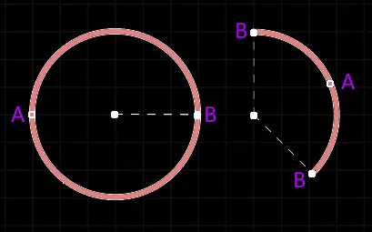
選択されたアーク
-
Aをクリックしてドラッグすると、半径を調整できます。
-
Bをクリックしてドラッグすると、終点(開始角度と終了角度)を調整できます。
-
編集ハンドルから離れた弧上のどこかをクリックしてドラッグすると、位置を変更できます。または、弧の中心点をクリックしてドラッグします。ドラッグ中に、弧を回転させたり、反転させたりできます:
アークのプロパティ

PropertiesのArcモード。
ネット情報
この領域では、アークが属するネットに関する情報、およびそのネットがメンバーである場合の差動ペアやxSignalについての情報が提供されます。適切な場合はクラス情報が表示されます。Delay、Length、Max Current、およびResistanceの値も提供されます。
PCB配置&編集テクニックのページを参照して、ネット情報についてさらに学びましょう。
位置
この領域の右側にある

アイコンは、以下のフィールドにアクセスするためには

(ロック解除)として表示される必要があります。ロック/ロック解除アイコンを切り替えて、そのロック状態を変更します。
-
(X/Y)
-
X(最初のフィールド)- このフィールドは、現在の原点に対してアークの中心の現在のX位置を示します。フィールド内の値を編集して、現在の原点に対するアークの位置を変更します。値はメートル法またはインペリアル法で入力できます。現在のデフォルトでない単位の値を入力する場合は、単位を含めてください。デフォルトの単位(メートル法またはインペリアル法)は、設計スペースでオブジェクトが選択されていないときにアクセスされるボードモードのプロパティパネルのその他領域の単位設定によって決定され、単位が指定されていない場合に使用されます。
-
Y(2番目のフィールド)- このフィールドは、現在の原点に対してアークの中心の現在のY位置を示します。フィールド内の値を編集して、現在の原点に対するアークの位置を変更します。値はメートル法またはインペリアル法で入力できます。現在のデフォルトでない単位の値を入力する場合は、単位を含めてください。デフォルトの単位(メートル法またはインペリアル法)は、設計スペースでオブジェクトが選択されていないときにアクセスされるボードモードのプロパティパネルのその他領域の単位設定によって決定され、単位が指定されていない場合に使用されます。
プロパティ
-
Component – このフィールドは、選択したアークが PCB コンポーネントの構成部品であり、親 PCB コンポーネントの指定子を表示している場合にのみ、PCB エディタに表示されます。クリック可能なComponent リンクを選択して、親コンポーネントのPropertiesパネルのComponentモードを開きます。
-
Net – アークのネットを選択するために使用します。アクティブボードデザインのすべてのネットがドロップダウンリストに表示されます。オブジェクトの配置が、既にNetに接続されている既存のオブジェクトと同じ位置から開始される場合、新しいオブジェクトのNetプロパティは自動的にそのネットに割り当てられます。No Netを選択して、アークがどのネットにも接続されていないことを指定します。プリミティブのNetプロパティは、PCB オブジェクトが正しく配置されているかどうかを判断するために、デザイン ルール チェッカーによって使用されます。または、Assign Netアイコン()をクリックしてデザイン空間内のオブジェクトを選択し、そのオブジェクトのネットが選択したアークに割り当てられます。
-
Layer - このフィールドには、アークが現在割り当てられているレイヤーが表示されます。アークは、使用可能な任意のレイヤーに割り当てることができます。割り当てられたレイヤーを変更するには、フィールドをクリックし、ドロップダウン リストからレイヤーを選択します。
-
Width - このフィールドには、アーク線の幅が表示されます。必要に応じて、幅に別の値を入力します。
-
Radius - このフィールドには、中心点からアーク線の中心までの距離を計測したアークの半径が表示されます。必要に応じて、半径に別の値を入力します。
-
Start Angle - このフィールドには、第 1 象限 (平面ジオメトリ) の X 軸から計測されたアークの開始角度が表示されます。必要に応じて、開始角度に別の値を入力します。
-
End Angle - このフィールドには、アークの終了角度が表示されます。必要に応じて、終了角度に別の値を入力します。
-
Propagation Delay - このフィールドには、信号がそのルートに沿って伝播するのにかかる時間が表示されます。
ペーストマスク拡張
はんだマスク拡張
選択したオブジェクトをトラックとアークでアウトラインする
メインメニューのTools » Outline Selected Objectsコマンドを使用して、デザイン内の選択されたフリープリミティブの周りにトラックとアークのアウトラインを配置することができます。この機能は、アウトラインをグラウンドソースに接続することで、重要なネットを電気的に隔離したい場合に特に便利です。コマンドを起動すると、オブジェクトはトラックまたはアークでアウトラインされます。アウトラインのトラック/アークは、幅8milで配置され、NetプロパティはNo Netに設定されます。
クリアランス、幅、およびショートサーキットの設計ルールがデザインに適用されるため、クリアランス違反はデザインルールチェッカーによってフラグが立てられます。
四角形の扱い
四角形は任意のレイヤーに配置することができます。さまざまなサイズの四角形を組み合わせて、不規則な形状のエリアを覆うことができますし、トラックやアークセグメントとも組み合わせることができます。
四角形は、非電気レイヤーにも配置できます。例えば、自動配線のための「進入禁止」エリアを指定するために、禁止領域レイヤーに四角形を配置します。パワープレーン、はんだマスク、またはペーストマスクレイヤーに四角形を配置して、そのレイヤー上にボイドを作成します。

配置された四角形
四角形は、PCBエディタおよびPCBライブラリエディタの両方で、以下の方法で配置することができます:
コマンドを起動した後、カーソルは十字線に変わり、四角形の配置モードに入ります。配置は、以下の一連のアクションを実行することで行われます:
-
四角形の最初の角を固定するために、クリックまたはEnterを押します。
-
カーソルを動かして四角形のサイズを調整し、次にクリックまたはEnterを押して、対角線上の反対側の角を固定し、四角形の配置を完了します。
-
さらに四角形を配置するか、右クリックまたはEscを押して配置モードを終了します。
配置中に実行できる追加のアクションは以下の通りです:
-
Tabキーを押して配置を一時停止し、PropertiesパネルのRectangleモードにアクセスして、そのプロパティをその場で変更できます。配置を再開するには、デザインスペースの一時停止ボタンオーバーレイ ( ) をクリックします。
-
Spacebarを押して、さまざまなコーナーモードをサイクルします。Rectangleを選択して直角のコーナー、Filletを選択して丸みを帯びたコーナー、またはChamferを選択して斜め/角度のあるコーナーにします。
-
+キーと-キー(テンキー上)を押して、設計内のすべての可視レイヤーを前後にサイクルし、配置レイヤーを迅速に変更します。
-
Altキーを押し続けると、移動の方向が最初の移動方向に応じて水平または垂直軸に制約されます。
配置中に属性を変更できます(Tabキーを押してプロパティパネルを開く)、これらはさらなる配置のデフォルト設定になることを念頭に置いてください。ただし、PreferencesダイアログのPCB Editor – DefaultsページにあるPermanentオプションが有効になっている場合は、変更は配置中のオブジェクトとその後に配置されるオブジェクトにのみ影響します。
グラフィカルな編集方法では、配置された矩形オブジェクトをデザインスペース内で直接選択し、そのサイズ、形状、または位置をグラフィカルに変更できます。
矩形オブジェクトが選択されると、次の編集ハンドルが利用可能になります。
 選択された四角形
-
四角形の角(A)をクリックしてドラッグすると、縦横同時に四角形のサイズを変更できます。
-
四角形の辺の中心(B)をクリックしてドラッグすると、縦または横方向に四角形のサイズを個別に変更できます。
-
編集ハンドルから離れた四角形の任意の場所をクリックしてドラッグすると、その位置を変更できます。ドラッグ中に、四角形は回転または反転させることができます:
四角形オブジェクトを元のプリミティブパーツのセットに変換するには、メインメニューからTools » Convert » Explode Rectangle to Free Primitivesコマンドを選択してください。分解された四角形を再グループ化する実際のコマンドはありませんが、Undoコマンドを使用してこれを実現できます。
四角形のプロパティ

PropertiesパネルのRectangleモード。
位置
この領域の右側にあるロックアイコンは、以下のフィールドにアクセスするためにはロック解除されている必要があります。ロック/ロック解除アイコンを切り替えて、そのロック状態を変更します。
プロパティ
-
Corner Mode - ドロップダウンから次のオプションの中から望ましい四角形のコーナーモードを選択します:
-
Rectangle - 配置された四角形が直角のコーナーを持つことを指定します。
-
Fillet - 配置された四角形が丸みを帯びたコーナーを持つことを指定します。
-
Chamfer - 配置された四角形が斜めまたは角度のあるコーナーを持つことを指定します。
コーナーモードは、配置中にSpacebarを押すことで選択することもできます。
-
Track Width - 現在のトラックの幅を表示します。このフィールドを編集して、トラック幅を0.001milから10000milの範囲内で変更します。
-
Fillet/Chamfer Size - これは、Corner ModeのドロップダウンからFilletまたはChamferが選択された場合、または配置中にフィレットまたはチャンファーモードが選択された場合にのみ利用可能です。
-
Layer - 現在四角形が割り当てられているレイヤー。四角形は利用可能な任意のレイヤーに割り当てることができます。ドロップダウンを使用して異なるレイヤーを選択します。
-
Width - 選択された四角形の(X軸の)幅を表示します。
-
Height - 選択された四角形の(Y軸の)高さを表示します。
-
 - このアイコンをクリックして、四角形の既存のX対Yの比率を保持します。
