電子設計とは、論理設計を回路図に取り込み、その設計を PCB 設計空間のオブジェクトの集合として表現するプロセスです。小さな回路であっても、回路図には多くのコンポーネントが含まれ、それぞれに多数のモデルやパラメータがあります。PCBデザインスペースはまた、ボードを構成する多数のデザインオブジェクトを含むことができます。デザインプロセスの過程で、様々なデザイン要件のバランスを取るために、これらのオブジェクトの配置やプロパティを変更する必要があります。
オブジェクトの配置と編集の共通点
Altium Designer では、オブジェクトを配置するプロセスは、配置するオブジェクトに関係なくほぼ同じです。最も単純なレベルでは、次のようなプロセスです:
-
配置するオブジェクトを選択します:
-
Place メインメニューからコマンドを選択します。
-
アクティブバー からコマンドを選択します。
-
デザインスペースで右クリックし、コンテキストメニューのPlace サブメニューからコマンドを選択します。
-
マウスを使用して、回路図エディタのデザインスペースに配置するオブジェクトの位置とサイズ(該当する場合)を指定します。
-
右クリック(またはEsc )を押してコマンドを終了し、配置モードを終了します。
回路図シート境界の外側に回路図デザインオブジェクトを配置することができ、そのようなオブジェクトを選択して移動することができます。回路図シートの境界外にあるオブジェクトを選択すると、回路図シートの境界内にあるオブジェクトと同じ操作やコマンドを実行できます。
デザインオブジェクトの配置
回路図デザインオブジェクトを配置する基本的な手順を以下に示します。
-
配置したいオブジェクトの種類を、Place メニューから選択するか(例:Place " Wire )、Activeツールバーのアイコンをクリックして選択します。配置のためのショートカットキーも利用できます(例えば、 P,W でワイヤを配置)。コンポーネント(部品)を配置するには、ComponentsパネルのPlaceボタンをクリックするか、Componentsパネルの利用可能なライブラリからコンポーネント名を選択し、ドキュメントにドラッグすることもできます。
-
オブジェクトを選択して配置すると、カーソルが十字に変わり、編集モードであることを示します。
-
配置する前にオブジェクトのプロパティを編集するには、Tabキーを押します。これにより、その特定のオブジェクトのPropertiesパネルが開き、様々なオプションを変更することができます。プロパティの設定が終わったら、
 をクリックして、配置モードに戻ります。配置中に編集する利点は、デジグネータのような数値の識別子を持つオブジェクトは自動インクリメントされることです。
-
カーソルを置き、左クリックするか、Enter を押して、オブジェクトを配置します。ワイヤーや多角形のような複雑なオブジェクトの場合、オブジェクトのすべての頂点を配置するために、位置とクリックの手順を続ける必要があります。
注意:
Preferencesダイアログの
Schematic - AutoFocus ページのオプションは、回路図の表示状態を制御します。例えば、接続されたオブジェクトを配置または編集するときに、回路図を自動的にズームインしたり、現在配置されているワイヤに関係のないすべての配線を暗くしたりすることができます。その他のズームやパンオプションは、ショートカットキーやマウスホイールを使用します。
Ctrlキーとホイール・マウスのスクロールでズーム・インとズーム・アウトができ、配置時にホイール・ボタンを押しながらマウスを上に動かすとズーム・イン、下に動かすとズーム・アウトします。マウスの動作は、
Preferencesダイアログの
System - Mouse Wheel Configuration ページで設定できます。
-
オブジェクトを配置した後、配置モード(十字カーソルで表示される)に残り、同じタイプの別のオブジェクトをすぐに配置できます。配置モードを終了するには、右クリックするか、Escキーを押します。ポリゴンを配置する場合など、オブジェクトの配置を終了するときと、配置モードを終了するときの 2 回、この操作を行う必要がある場合があります。配置モードを終了すると、カーソルはデフォルトの形状に戻ります。
Editing Prior to Placement
オブジェクトのデフォルトプロパティ(論理的にあらかじめ定義されているプロパティ)は、PreferencesダイアログのSchematic - Defaults ページでいつでも変更できます。これらのプロパティは、後続のオブジェクトを配置するときに適用されます。

Primitive List 列を使用してオブジェクトのプロパティにアクセスし、必要に応じてデフォルト値を編集します。
オブジェクトのデフォルト値は、デフォルトでは、ファイルAdvsch.dft に保存されます。オプションとして、値を別の名前で.dft ファイルに保存することもできます。dft ファイルを保存およびロードするためのコントロールが用意されており、お気に入りのデフォルト・オブジェクト値「セット」を作成することができます。.dft ファイルに保存された設定や、. dft ファイルから読み込まれた設定は、すべてユーザー定義のデフォルト値です。必要であれば、 Set To Defaults またはReset All オプションを使って、いつでも元のデフォルト値に戻すことができます。元のデフォルト値はハードコードされています。
Editing During Placement(配置中の編集)
オブジェクトが最初に配置されるとき、多くの属性が編集可能です。これらの属性にアクセスするには、配置モードでTabキーを押して、関連するProperties パネルを開きます。Tabキーを押すと、配置が一時停止され、オブジェクトに必要な編集ができるようになります。

例Net Label オブジェクトのProperties パネル。
編集が終わったら、デザインスペースの一時停止ボタンオーバーレイ () をクリックして配置を再開します。
この方法で設定された属性は、
Preferencesダイアログの
Schematic - Defaults ページの
Permanentオプションが有効になっていない限り、それ以降のオブジェクト配置のデフォルト設定になります。このオプションが有効な場合、変更は配置中のオブジェクトと、同じ配置セッション中に配置された後続のオブジェクトにのみ影響します。
Editing After Placement
オブジェクトが配置されると、それを編集する方法がいくつかあります。以下に説明します。
関連するプロパティパネルまたはダイアログ
この編集方法では、関連するProperties パネルモードとダイアログを使用して、配置されたオブジェクトのプロパティを変更します。
配置後、関連するダイアログには次の方法でアクセスできます:
-
配置されたオブジェクトをダブルクリックします。
-
カーソルをオブジェクトの上に置き、右クリックし、コンテキストメニューからProperties を選択します。
配置後、Properties パネルの関連モードには、次のいずれかの方法でアクセスできます:
-
Properties パネルがすでにアクティブな場合は、オブジェクトを選択します。
-
オブジェクトを選択した後、デザインスペースの右下にあるPanels ボタンからProperties パネルを選択するか、メインメニューからView " Panels " Properties を選択します。
Preferences ダイアログの
Schematic - Graphical Editing ページ で、
Double Click Runs Interactive Properties オプションが無効(デフォルト)になっている場合、プリミティブをダブルクリックするか、選択したプリミティブを右クリックして
Properties を選択すると、ダイアログが開きます。
Double Click Runs Interactive Properties オプションを有効にすると、
Properties パネルが開きます。
ダイアログとパネルのオプションは同じですが、オプションの順序と配置は若干異なります。
Ctrl+Q を押すと、パネル/ダイアログで現在使用されている測定単位をメートル法(mm )とインペリアル法(mil )の間で切り替えることができます。これは、パネル/ダイアログの測定値の表示にのみ影響します。シートに指定された測定単位は変更されません。これは、デザインスペースでオブジェクトが選択されていないときに、Properties パネルのUnits 設定で構成されます。
グラフィカル編集
この編集方法では、配置されたオブジェクトをデザインスペースで直接選択し、そのサイズ、形状、位置をグラフィカルに変更することができます。形状やサイズの変更は、オブジェクトが選択されると表示される編集ハンドルで行います。
オブジェクトが選択されると、そのオブジェクトを移動したり、グラフィカルな特性を編集することができます。オブジェクトをクリックして選択すると、その「ハンドル」や頂点が表示されます。選択されたオブジェクトは、PreferencesダイアログのSchematic - Graphical Editing ページ の Color Options領域のSelectionsフィールドで定義された選択色でハイライトされます。選択したオブジェクトをグラフィカルに変更するには、編集ハンドルをクリックしたままにします。オブジェクトのその点がカーソルにくっつきます。マウスを新しい場所に移動して放すと、サイズが変更されます。選択したオブジェクトのどこかをクリックして移動するか、Deleteキーを押して削除します。
選択したオブジェクトの移動:
-
選択した回路図または PCB オブジェクトは、Ctrlキーを押しながら矢印キーを押すことで、現在のスナップグリッド値で 'nudged' することができます。
-
選択したオブジェクトは、Ctrl+Shift キーを押しながら矢印キーを押すことで、スナップグリッド値 x10 で 'nudge' することもできます。
-
回路図オブジェクトでは、現在のスナップグリッドがステータスバーに表示されます。利用可能なスナップグリッドは、Preferences ダイアログのSchematic - Grids ページで設定します。G を押して、使用可能なグリッド値を循環させながら作業します。
-
PCB オブジェクトの場合、現在の Snap Grid はステータスバーに表示され、Grid Editor ダイアログで定義されます。Ctrl+G を押してダイアログを開き、新しい値を入力します。
-
Reposition Selected Components コマンド(Tools " Component Placement " Reposition Selected Components またはショートカットT,O,C )を使用して、複数の PCB コンポーネントを選択し、個別に(選択した順番に)再配置できます。コンポーネントは、PCBパネルを使用して PCB 上で直接選択するか、Cross Select Mode が有効な場合、回路図エディタで選択できます (Tools メニュー)。
オブジェクトの再配置
オブジェクトをグラフィカルに再配置する場合、2 つの用語が使用されます:移動 とドラッグ 。
-
移動 - オブジェクトの接続性を無視して移動します。
-
Drag - オブジェクトを移動しながら、接続性を維持します。
回路図エディタは、Always Drag オプション (Schematic - Graphical Editing pagePreferences ダイアログの ) の現在の状態に応じて、どちらかのモードで動作します。
Always Drag オプションの現在の状態は、Ctrl キーを押しながら作業することで一時的に切り替えることができます。Always Drag オプションが有効で、Ctrl + クリック、ホールド、ドラッグした場合、ソフトウェアは接続を維持しようとせず、代わりにカーソル下のオブジェクトを移動します。この場合、そのオブジェクトがユニオンのメンバーであれば、ユニオン内のすべてのオブジェクトが移動します。Always Drag を有効にして作業する場合は、Ctrl を押しながらクリック&ドラッグすると、ユニオン内のすべてのオブジェクトが移動します。 Always Drag が無効になっている場合、 Ctrl を押すと、オブジェクトの移動からドラッグに切り替わります。
オブジェクト(または選択中のオブジェクトの1つ)をクリックしたまま、位置を変更します。その際、カーソルはオブジェクトのクリックした場所とは異なる場所にスナップします。これは意図的なもので、 Preferences ダイアログの Schematic - Graphical Editing ページ で設定される以下のオプションによって制御されます。 Always Drag オプションがオンの場合、ネットラベル、シートシンボル、コンポーネントなどの電気的オブジェクトは、矩形や線などの非電気的オブジェクトとは動作が異なることに注意してください。
Center of Object - 有効にすると、グラフィカルオブジェクトの場合、カーソルを移動し、オブジェクトの幾何学的中心でホールドします。電気的オブジェクトの場合、 Always Drag オプションが有効になっていれば、クリック位置でホールドします。 Always Drag がオフの場合は、幾何学的中心でホールドする。テキスト文字列の場合は、文字列の参照点(文字列の現在の Justification プロパティの設定によって決まります)で保持します。
Object's Electrical Hot Spot - 有効にすると、オブジェクトが電気的オブジェクトの場合、ホットスポットでホールドします(ホットスポットは、接続性が作成されるポイントです)。有効にすると、このオプションは、電気的オブジェクトの Center of Object オプションを上書きします。
Always Drag - Drag という用語は、接続性を維持しながら 移動することを示すために使用されます 。このオプションを有効にすると、電気オブジェクトをクリックしてドラッグしたときに、現在の接続性を維持し、ドラッグに合わせて配線を適切に調整するようにソフトウェアに要求します。 Ctrl を押したままにすると、ドラッグから移動に一時的に切り替わります。
Always Drag が有効な場合、ソフトウェアはそのネットで現在定義されている接続性を維持しようとします。Always Drag は、 Ctrl を押しながらクリック&ドラッグすることで、一時的に無効にすることができます。
オブジェクトの移動中に G キーを押すと、利用可能な Grid Preset 設定を循環させることができます。これらは Preferences ダイアログの Schematic - Grids ページで設定します。
テキストまたはグラフィカルオブジェクトの移動中に Ctrl キーを押すと、現在の Grid Preset が一時的に無効になり、グリッドが最小の 10mil 値に設定されます。この機能は、テキスト文字列の位置を注意深く調整する必要がある場合に便利です。
選択したオブジェクトは、 Ctrl+Arrow キーを押すことで、(現在のスナップグリッド値に従って)1グリッド分「ナッジ」することができます。選択されたオブジェクトは、 Ctrl+Shift+arrow キーを押すことで、10グリッド分(スナップグリッド値×10倍)「ナッジ」させることもできる。
移動中に Alt キーを押すと、最初の移動方向に応じて、移動方向が水平軸または垂直軸に拘束される。
Ctrl+Spacebar を押すと、選択範囲を反時計回りに90°刻みで回転させることができる。 Shift+Ctrl+Spacebar を押すと、選択範囲が時計回りに回転する。
X または Y キーを押すと、それぞれ X 軸または Y 軸に沿って選択範囲が反転します。
スペースバー (または Shift+Spacebar ) を押して、接続されているワイヤ、バス、または信号ハーネスの配線モードを変更します。接続された配線の配線モードは、 Drag Orthogonal オプションが有効になっている場合にのみ変更できます。 Schematic - General ページ Preferences ダイアログにあります。デフォルトのモードは、配線を90度の角度に保ちます。このオプションを無効にすると、配線モードが循環しないだけでなく、接続された配線が斜めに再配置されます。
移動コマンド オブジェクトの位置は、メインメニューの 編集 " 移動 サブメニュー、または アクティブバー の移動サブメニューのコマンドを使用して変更できます。
Drag - 他の電気的オブジェクト(電気的オブジェクトが選択されている場合)との接続を維持しながら、現在のドキュメント内の個々のオブジェクトをドラッグします。
Move - 現在のドキュメント内の個々のオブジェクトを移動します。この機能を使用する場合、接続性は維持されません。
Move Selection - 現在のドキュメントで選択されたオブジェクトを再配置します。この機能を使用しても、接続性は維持されません。
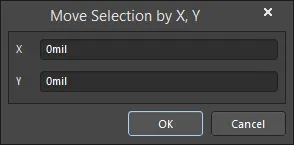
Move Selection by X, Y - 現在の選択オブジェクトを X 方向および Y 方向に正確な量だけオフセットします。コマンドを起動すると、 Move Selection by X, Y ダイアログが表示されます。このダイアログを使って、選択範囲を移動させるためのデルタXやデルタYの増分値を指定します。 OK をクリックすると、選択範囲が移動します。
Move Selection by X, Y ダイアログ Drag Selection - 現在のドキュメントで選択された電気的オブジェクトを、他の電気的オブジェクトとの接続を維持しながらドラッグします。非電気的オブジェクトの選択範囲で使用するには、 Ctrl キーを押したまま移動を開始します。これにより、 Always Drag オプションが一時的に無効になり、 Drag Selection コマンドが、 Move Selection コマンドとして動作するように切り替わります。移動が始まったら Ctrl キーを離すと、グリッドのスナップが復活します。
Move To Front - このコマンドは、オブジェクトの位置を変更し、現在のドキュメントの図面スタック内の他のすべてのオブジェクトの前面に配置するために使用します。
詳しくは Drawing Stack 内のオブジェクトの移動 を参照してください。
Rotate Selection - このコマンドは、1つまたは複数の選択されたオブジェクトを反時計回りに回転させるために使用します。
Rotate Selection Clockwise - このコマンドは、1 つまたは複数の選択されたオブジェクトを時計回りに回転させるために使用します。
整列コマンド オブジェクトは整列を変えて移動することもできます。オブジェクトを他のオブジェクトと整列させるには、整列させたいオブジェクトをすべて選択し、選択したオブジェクトを右クリックし、 Align を選択します。あるいは、メインメニューの Edit " Align サブメニューか、 Active Bar の Alignment サブメニューを使います。整列サブメニューには、選択したオブジェクトを分散させるための多くのオプションが含まれています。
整列中は接続性は保持されません。
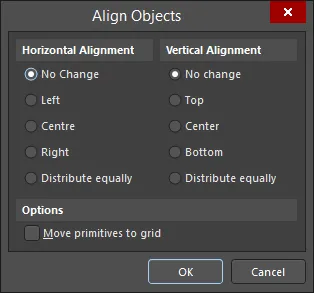
Align コマンドを使用して、 Align Objects ダイアログにアクセスします。このダイアログには、現在選択されているデザインオブジェクトのセットを必要に応じて素早く整列させるためのコントロールが用意されています。ダイアログを使用して、必要に応じて選択したオブジェクトの垂直および/または水平アライメントのオプションを設定し、 OK をクリックしてアライメントを実行します。
Align Objects ダイアログ
Horizontal と Vertical の両方のオプションを同時に有効にすると、選択したオブジェクトが重なってしまい、コンフリクトが発生する場合があります。
Distribute equally オプションを使うと、移動オブジェクトがグリッドから外れることがあります。 Move primitives to grid オプションを有効にすると、アライメントが完了した後、選択内のすべてのプリミティブが有効なグリッドポイントに位置するようにアライメントを制限できます。
オブジェクトの整列ダイアログのオプションとコントロール
水平方向の整列 - 選択したオブジェクトの水平方向の整列を以下のオプションから選択します。 変更なし - オブジェクトの水平方向の整列を変更しない。 左 - オブジェクトを一番左のオブジェクトの左端に整列させる。中央 - 選択範囲内の左端と右端のオブジェクトの中間を軸にオブジェクトを配置します。 右 - 右端のオブジェクトの右端にオブジェクトを配置します。 均等に配置 - 左端と右端のオブジェクトをそれぞれ左と右の境界として、選択したオブジェクトを水平方向に均等に配置します。 垂直方向の配置 - 選択したオブジェクトの垂直方向の配置を以下のオプションから選択します:
No Change - 選択されたオブジェクトの垂直方向の配置を変更しません。 Top - オブジェクトを一番上のオブジェクトの上端に揃えます。 Center - 選択範囲内の一番上のオブジェクトと一番下のオブジェクトの中間の軸にオブジェクトを揃えます。 Bottom - オブジェクトを一番下のオブジェクトの下端に揃えます。均等に配置 - 選択されたオブジェクトを垂直方向に均等に配置します。一番上と一番下のオブジェクトをそれぞれ上と下の境界線として使用します。 プリミティブをグリッドに移動 - このオプションを有効にすると、アライメントが完了した後、選択範囲内のすべてのプリミティブが有効なグリッドポイント上に配置されます。
Align Left / Align Right / Align Top / Align Bottom コマンドを使用すると、選択したデザインオブジェクトをそれぞれ左/右/上/下のエッジで整列できます。コマンドを起動すると、一番左/右/上/下のオブジェクトの左/右/上/下のエッジが基準として使用され、選択範囲内の他のすべてのオブジェクトは、その左エッジがこの基準に揃うように、左/右/上/下に移動します。
オブジェクトは参照に対する位置に関係なく移動します。オブジェクトの一部または全体が重なってしまう可能性があります。
Align Horizontal Centers / Align Vertical Centers コマンドを使うと、選択したオブジェクトを1つの列/行に、水平/垂直の中心で揃えて配置することができます。このコマンドを実行すると、選択範囲内のオブジェクトが水平/垂直に移動し、水平/垂直の中心で整列された1つの列/行を形成します。列の垂直方向の中心線は、選択範囲の最左端と最右端のオブジェクトの中間点です。行の水平方向の中心線は、選択範囲の最上端と最下端のオブジェクトの中間点です。
Distribute Horizontally / Distribute Vertically コマンドを使うと、選択オブジェクトの水平/垂直方向の間隔を等しくすることができます。このコマンドを実行すると、選択範囲の一番左と一番右、一番上と一番下のオブジェクトの位置は固定され、他のすべてのオブジェクトの間隔は等しくなります。オブジェクトの垂直/水平位置は変更されません。
Align To Grid コマンドは、選択したオブジェクトを現在のスナップグリッド上の最も近い点に移動するために使います。
オブジェクトの座標を丸める メインメニューから Tools " Convert " Round coordinates of objects コマンドを選択することで、デザインの途中で測定単位をインペリアルからメトリックに切り替えたときの丸め効果に対抗するために、オブジェクトの内部座標を丸めることができます。全体的な結果として、すべてのデザインオブジェクトの内部座標は、最初からメートル単位でデザインを開始していた場合と同じになります。
コマンドを起動すると、 Rounding coordinates of objects ダイアログが表示されます。このダイアログを使用して、丸め処理を適用するドキュメントを定義します:
このドキュメントのみ - 現在のドキュメントの座標のみを丸めます。
現在のプロジェクトのすべての回路図ドキュメント - 現在のプロジェクトのすべての回路図ドキュメントのラウンド座標。現在閉じている現在のプロジェクトの回路図ドキュメントが開かれます。
All open schematic documents - 所属プロジェクトに関係なく、現在開いているすべての回路図ドキュメントの丸め座標。
オブジェクトの座標を丸める ダイアログ 選択して、 OK をクリックすると、情報ダイアログが開き、いくつのドキュメント上のいくつのオブジェクトの座標が丸められたかをまとめます。
図面スタック内のオブジェクトの移動 回路図エディタは、オブジェクト、テキスト、グラフィックを自動的にレイヤーにスタックします。各オブジェクトは作成順序によって異なるレイヤーにあるため、オブジェクトが重なるように配置することが可能です。最近作成または追加されたオブジェクトは、常に一番上のレイヤーにあります。
メインメニューの Edit " Move サブメニュー、または Active Bar の Move サブメニューの以下のコマンドを使うことで、このオブジェクトが一部である重なり合ったオブジェ クトスタック内のオブジェクトを移動させることができます。
Bring To Front / Send To Back - 重なっているオブジェクトのスタックの一部であるオブジェクトを、そのスタック内の他のすべてのオブジェクトの前面/背面に移動します。コマンドを起動したら、移動したいオブジェクトをクリックします。オブジェクトは、その x 座標または y 座標を変更することなく、スタックの一番上/一番下に、重なっているすべてのオブジェクトの前/後ろに移動します。
Bring To Front Of / Send To Back Of - 重なっているオブジェクトのスタックの中で、あるオブジェクトを他のオブジェクトの前 / 後ろに移動します。コマンドを起動したら、移動させたいオブジェクトをクリックし、次に最初のオブジェクトを前/後ろに移動させたい「ターゲット」オブジェクトをクリックします。最初のオブジェクトは、そのx座標やy座標を変えずに、このターゲットオブジェクトの前/後ろに移動します。
初期オブジェクトやターゲットオブジェクトを選択するとき、複数のオブジェクトが重なっている場所をクリックすると、重なっているすべてのオブジェクトを含むポップアップが表示され、そこから目的のオブジェクトを選択することができます。
インプレース・テキスト編集 インプレース・テキスト編集では、 プロパティ パネルから編集するのではなく、指示子やコメントテキスト、テキスト文字列、テキストフレーム、完全に展開されたノートなど、現在のドキュメント上のテキスト項目を直接編集することができます。これを行うには、テキストオブジェクトを一度クリックして選択し、少し待ってからもう一度クリックしてインプレース編集モードにします(2回のシングルクリックを1回のダブルクリックと解釈して プロパティ パネルを開いてしまわないように、各クリックの間に十分な時間を置く必要があります)。または、インプレース編集を行うテキストオブジェクトを選択し、 F2 キーボードショートカットを使用します。編集したいテキストオブジェクトを選択し、コマンドをアクティブにすると、テキストが強調表示され、直接編集できるようになります。
インプレース・テキストの編集を終了するには、テキスト文字列から離れたところでクリックします。パラメータテキストやテキスト文字列の場合は、 Enter を押すこともできます。テキストフレームや注釈の場合は、緑のチェックボタン を押すことができます(加えた変更が必要ないと判断した場合は、赤の十字ボタン を押して変更を破棄します)。
この機能は、 Preferences ダイアログの Schematic - General ページ で、 Enable In-Place Editing オプションが有効になっている場合にのみ使用できます。このオプションが無効の場合、親オブジェクトを選択し、 Properties パネルからテキストを編集する必要があります。
右クリックメニューには、 Cut 、 Copy 、 Paste 、 Delete などの標準的な編集コマンドがあります。
テキストストリング、テキストフレーム、およびノートの詳細については、 Working with Text Objects on a Schematic ページを参照してください。
ポリラインオブジェクトの編集 回路図シート上に配置されたポリライン接続オブジェクト(ワイヤ、バス、またはシグナルハーネス)のセグメントは、メインメニューから Edit " Break Wire コマンドを使用して、回路図シート上の選択した位置で2つに分割することができます。コマンドを起動すると、 Preferences ダイアログの Schematic - Break Wire ページ の Cutter Box 、および Extremity Markers の設定に従ってカーソルが表示されます。
カッターボックスが表示されないように設定されている場合、またはカーソルがポリラインセグメントを通過するときのみ表示されるように設定されている場合、カーソルがワイヤセグメントから離れている間、中央の十字マーカーを使用して切断領域がワークスペースで区別されます。カッターボックスと四辺のマーカの両方が表示されないように設定されている場合、カーソルを線分上に通過させると、その線分の該当部分または全体がハイライトされます。
効果的に 2 つに分割したいワイヤー、バス、またはシグナルハーネスのセグメント上にカーソルを置き、クリックするか、 Enter を押します。指示された長さのセグメントが削除され、セグメントが 2 つに分割されます。
さらにポリラインオブジェクトのブレークを続けるか、右クリックするか、 Esc を押して終了します。
ブレイクワイヤーモードで、 スペースバー を押すと、以下の切断長モードが切り替わります:
Snap To Segment - このモードでは、カッターはポリラインセグメント全体にスナップするように自動サイズ調整されます。
Snap Grid Size Multiple - このモードでは、カッターは現在のスナップ グリッドの定義された倍数にサイズ調整されます。
固定長 - このモードでは、カッターは定義された固定長にサイズ調整されます。
カッターのサイズに関係なく、 Snap To Segment 以外のオプションを使用すると、 Snap To Segment が選択されているかのように、カッターは小さいサイズのワイヤーセグメントを通過するときに、その全体が収縮します。
カッティングツールのプロパティは、 Preferences ダイアログの Schematic - Break Wire ページで定義できます。ローカルドキュメントレベルで変更された値は、即座に環境設定レベルに反映されます。
また、 Delete キーをタップすることで、選択したワイヤセグメント(バスやシグナルハーネスオブジェクトのセグメントではない)を削除することができます。オートジャンクションにも対応しており、そのジャンクションまでのワイヤセグメントのみを削除することができます(他の2つのワイヤセグメントが接続されたままになっている場合は、そのジャンクションを含む)。特定のワイヤセグメントを2回クリック(その間は一時停止)するだけで、そのセグメントが選択され、終点の編集ハンドが赤くなります。異なるワイヤにまたがる複数のセグメントを削除することもできます。各セグメントが選択されていることを確認してください( Shift +各セグメントを2回クリックすると、全体のセグメント選択に含まれます)。
回路図シートまたは回路図シンボル上に配置された親ポリゴン、ライン、ワイヤ、バス、シグナルハーネス、またはラインオブジェクトに対して、現在カーソルの下にある特定の頂点を編集するには、必要な頂点の右クリックメニューからアクセスできる、 Edit Vertex n コマンドを使用します。コマンドを実行すると、親オブジェクトのプロパティを示すダイアログが表示されます。選択した頂点は、パネルの Vertices 領域で編集できるように選択されます。
Cut/Copy and Paste の使用 回路図エディタでは、回路図ドキュメント内またはドキュメント間でオブジェクトのカット/コピーやペーストができます。Windows のクリップボードにオブジェクトをカット/コピーし、他のドキュメントに貼り付けることができます。テキストをWindowsクリップボードから回路図のテキストフレームに貼り付けることができます。また、Microsoft Excel のような他のアプリケーションから、または Altium Designer 内のグリッドスタイルのコントロールから、テーブルタイプの選択範囲を直接コピー&ペーストすることができます。
Smart Paste 機能を使用して、より高度なコピー/貼り付け操作を実行できます。
カット/コピーしたいオブジェクトを選択し、メインメニューから Edit " Cut ( Ctrl+X ) / Edit " Copy ( Ctrl+C ) をクリックするか、右クリックメニューから Cut / Copy コマンドを選択し、貼り付け時にオブジェクトの正確な位置決めに使用されるコピー基準点をオブジェクト上に設定します。 Preferences ダイアログの Schematic - Graphical Editing ページで Clipboard Reference オプションが有効になっている場合のみ、参照点を設定するためにクリックするよう求められます。 Clipboard Reference オプションが無効になっている場合は、ショートカットを使用してコマンドを起動することをお勧めします。
コピーの一部としてシートテンプレート(ボーダー、タイトルブロックなどを含む)を追加する必要がある場合、 Preferences ダイアログの Schematic - Graphical Editing ページで、 Add Template to Clipboard オプションが有効になっていることを確認してください。
現在選択されているデザインオブジェクトをテキスト形式でクリップボードにコピーするには、オブジェクトを選択し、メインメニューから Edit " Copy As Text コマンドを選択します。選択範囲内のテキストベースのオブジェクト(注釈、ノート、テキストフレーム、ネットラベル、オフシートコネクタ、ポート、パワーポートなど)のテキストがクリップボードにコピーされます。この情報は、任意のテキストフィールドや外部テキストドキュメントに貼り付けることができます。
最後にクリップボードにカット/コピーした内容をアクティブなドキュメントに配置するには、メインメニューから Edit " Paste コマンドを選択するか、デザインスペース内で右クリックし、コンテキストメニューから Paste コマンドを選択します(ショートカット: Ctrl+V )。
Schematic - Graphical Editing Page of the Preferences ダイアログで、 Reset Parts Designators on Paste オプションが有効になっている場合、コピーしたコンポーネントオブジェクトをペーストすると、そのデジグネータはリセットされます。
選択した1つまたは複数のオブジェクトをコピーし、現在のドキュメント内の必要な場所に選択したオブジェクトの複数のインスタンスを貼り付けるには、メインメニューから Edit " Duplicate コマンドを使用することもできます(ショートカット: Ctrl+R )。このコマンドはオブジェクトのコピー&ペーストに使用されるため、グループオブジェクトの子オブジェクトの複製には使用できません。
スマートペーストの使用

-
-
-
-
-
-
-
-


回路図エディタのスマートペースト機能では、選択したオブジェクトのコピーをオプションで変換し、別のオブジェクトとして貼り付けることができます。例えば、選択したネットラベルをコピーし、ポートとしてスマートペーストしたり、選択したシートエントリのグループをポート+ワイヤ+ネットラベルとしてペーストし、バスを個々のワイヤに展開することができます。
スマートペーストに必要なオブジェクトがクリップボードにコピーされたら、メインメニューからEdit " Smart Paste コマンドを選択するか、Shift+Ctrl+V キーボードショートカットを使用してSmart Paste ダイアログにアクセスします。

Smart Paste ダイアログ
Options and Controls of the Smart Paste Dialog
Choose the Object to Paste
-
Schematic Object Type Grid - 選択したクリップボード内の全てのオブジェクトを種類別にグループ化したリストを表示します。チェックボックスで、どのオブジェクトを貼り付けるかを選択します。貼り付けを行う前に、ダイアログのChoose Paste Action 領域から操作を選択する必要があります。これにより、選択したオブジェクトが回路図シートにどのように配置されるかが決まります。Themselves ペースト操作は、選択したオブジェクトをクリップボードに貼り付ける標準的なペースト操作です。他の操作では、ペースト時にソースオブジェクトを別のオブジェクト(またはオブジェクトの集まり)に変換することができます。
-
Windows クリップボードコンテンツグリッド- ソフトウェアは独自のクリップボードを使用します。スマートペースト操作では、ソフトウェアのクリップボードとWindowsのクリップボードの両方でペースト操作を制御できます。Windowsクリップボードの内容をスマートペーストに含めたい場合は、有効にします。
Paste Action
-
Paste As - 貼り付けを行う前に、貼り付け操作を選択する必要があります。これにより、選択したオブジェクトが回路図シートにどのように配置されるかが決まります。Themselves ペースト操作は、標準的なペースト操作です。その他の操作では、ペースト時にソースオブジェクトを別のオブジェクト(またはオブジェクトの集まり)に変換することができます。
-
Ports, Sheet Entries, Net Labels は、等価なポート、シートエントリ、ネットラベル、または、1つのテキストフレーム/ノート、または、オブジェクトごとのポートとネットラベルセット(ワイヤ付き)に変換できます。
-
Label, Text Frame, Note は、ラベル、テキストフレーム、ノートに変換できます。
-
-
Windows Clipboard Graphics 画像に変換することができます。 Options - さまざまな Paste As オブジェクトを選択すると、さまざまなオプションが表示されます:
オプション Sort Order と Signal Names は、最も一般的なオプションです。これらのオプションは、オブジェクト Net Labels、Ports、Cross Sheet Connectors、Sheet Entries、Harness entries、およびこれらのオブジェクトのいずれかが使用されるすべてのグループを選択するときに使用できます。Option Sort Order を By Location に設定すると、コピーされたオブジェクト間のクリアランスが保持されます。 Alpha-Numeric を選択すると、名前はアルファベット順にソートされます。 Signal Names オプションについては、さらに多くの可能性があります。コピーした名前を変更したくない場合は、 Keep を選択します。 Expand Buses を選択すると、フリーのオブジェクトを持つことができます。また、 Group Nets with Lower First or Higher First というオプションを選択して、オブジェクトをバスのインデックスで貼り付けることもできます。このセクションの最後のオプションは、 Inverse Bus Indices で、コピーしたテキストのインデックスを逆にすることができます。例えば、 LEDS[ 7..0 ] という名前をコピーすると、 LEDS[ 0..7 ] として貼り付けることができます。 ポートを選択すると、 Port Width オプションを設定できます。 Use Default Size として設定すると、環境設定からその値が使用されます。また、 Set Width To Widest を選択すると、ポートの最も幅の広い値を取得できます。最後のオプションは Set Width To Fit で、テキストにぴったり合うように、正確なサイズでポートが作成されるように設定します。 いくつかのシートエントリを貼り付けることを選択すると、 Same Side オプションが表示されます。このオプションにより、コピーしたすべての情報をシート記号の片側に貼り付けることができます。このオプションがチェックされていない場合、シート項目はデフォルトの側を維持します。 Wire Length オプションは、オブジェクトのグループを選択するときに利用でき、配置されるワイヤの長さの値を入力できます。 ワイヤ間のクリアランスは、実際のグリッド値によって設定されます。 テキストフレームにテキストを貼り付ける場合、 Text Frame Size と Aspect Ratio を選択できます。こ の 2 番目のオプシ ョ ンは、 Set Width/Height using Aspect Ratio を設定した場合にのみ利用可能です。テキストフレームは、このアスペクト比で定義された寸法で配置されます。その他の場合は、このオプションを 「デフォルトのサイズを使用」 に設定して環境設定の値を使用するか、 「サイズを合わせて設定」 を選択して、テキストフレームが貼り付ける情報に合うようにします。 ハーネスコネクタとして情報を貼り付ける場合、オプション Harness Type を使用してコネクタに名前を付けることができます。ハーネスコネクタをポートで貼り付ける場合、 Port Name および Wire Length を入力することもできます。 Paste Array Enable Paste Array - 選択したオブジェクトを2次元の配列としてコピーできます。作成されるコピーの総数は、列数×行数です。 OK をクリックすると、配列が挿入されるドキュメント上の開始位置を選択するプロンプトが表示されます。カーソルを希望の位置に置き、 Enter をクリックまたは押します。
Columns Count - 貼り付け配列の列数を指定します。各列は、 Column Spacing の設定で区切られます。 Spacing - スペーシングに正の値または負の値を入力し、配列を水平に配置する場合は右または左に、垂直に配置する場合は上または下に貼り付けるかどうかを決定します。 Rows Count - 貼り付け配列に必要な行数を指定します。各行は、 Row Spacing 設定で区切られます。 Spacing - スペーシングに正の値または負の値を入力し、配列を水平配置の場合は右または左に、垂直配置の場合は上または下に貼り付けるかどうかを決定します。 Text Increment Direction - 貼り付けるコピーの文字列 (指示子など) をインクリメントする方法を選択します。 なし - インクリメントしません。各コピーは同じ文字列を持ちます。 水平方向の最初 - 文字列の値をその前任者から プライマリ 量だけ増加させることによって、文字列をインクリメントします。インクリメントする後継の文字列は、すぐ右のシーケンスで次の文字列を見つけることによって見つける。行が再シーケンスされたら、上の次の行の先頭に移動する。ピンは、 Secondary 設定を使用してインクリメントすることもできる。 Vertical First - 文字列の値を、 Primary の量だけ前任者から増やすことによって、文字列をインクリメントする。インクリメントする後継の文字列は、すぐ上のシーケンスで次の文字列を見つけることで見つける。列の並びが変わったら、右隣の列の先頭に移動する。ピンは、 Secondary (セカンダリ )設定を使用してインクリメントすることもできる。 Primary (プライマリ )-文字列は、 Primary (プライマリ )量だけ、前任者からインクリメント/デクリメントされる。ピンは、 Secondary 設定を使用して変更することもできます。 Secondary - 文字列は、 Primary の量だけ、前任者からインクリメント/デクリメントされます。ピンは、 Primary 設定を使用して変更することもできます。 Remove Leading Zeroes - このオプションを有効にすると、テキスト文字列から先頭のゼロが削除されます。例えば、このオプションを有効にすると、000ABCはABCとして変換されます。 配置されたオブジェクトの順序を逆にできるように、間隔フィールドに負の値を追加できます。
この機能を使用するには、基本的にダイアログの以下の3つの領域を必要に応じて設定する必要があります:
貼り付けるオブジェクトの選択 - このセクションには、クリップボードにあるすべてのオブジェクトのリストが、そのタイプ別にグループ化されて表示されます。それぞれの Schematic Object Type の横にあるチェックボックスを使用して、貼り付けるオブジェクトを選択します。Altium Designer は、クリップボードオブジェクトの詳細の解像度を上げるために、メインのウィンドウズクリップボードとは別のクリップボードを維持しますが、必要であれば、Windows クリップボードコンテンツを Smart Paste のソースとして使用することもできます。
新しいオブジェクトを貼り付ける前に、適切な Paste As オブジェクトを選択し、選択したオブジェクトがどのように変換されるかを定義する必要があります。 Themselves としてオブジェクトをペーストすると、標準的なペースト操作が実行されます。他のオプションは、ペーストする前に、ソースオブジェクトを選択したオブジェクト、またはオブジェクトのコレクションに変換します。その他のオプションがある場合は、選択したペーストオブジェクトの下に表示されます。
Paste Array - このオプションを有効にすると、選択したオブジェクトを2次元配列としてコピーします。作成されるコピーの総数は、列数×行数になります。識別子を含むオブジェクトについては、Text Increment コントロールを使用して、プライマリ(および該当する場合はセカンダリ)識別子のインクリメント方法を決定します。 Direction フィールドを使用して、 Horizontal First または Vertical First のように、インクリメントの適用方法を決定する。インクリメントなしで識別子の正確なコピーを得るには、方向を None に設定する。
Smart Paste ダイアログでオプションを設定すると、ダイアログの下部に Summary 領域が表示され、何が起こるか、つまり、指定されたクリップボードの内容に基づいてデザインスペースに何が貼り付けられるかの概要が表示されます。
必要に応じてオプションを設定し、 OK をクリックします。配列が配置されていない場合、ペーストされるコンテンツはカーソル上に浮いて表示されます。デザインスペース内の必要な位置にコンテンツを配置し、クリックするか、 Enter を押してペーストします。
リエントラント編集 回路図エディタには、リエントラント編集と呼ばれる強力な機能があり、現在実行中の操作を終了することなく、キーボードショートカットを使用して 2 番目の操作を実行できます。例えば、パーツを配置するときに スペースバー を押すと、オブジェクトが回転しますが、配置プロセスは中断されません。パーツを配置すると、カーソルに回転済みの別のパーツが表示されます。
リエントラント編集は、まだ配置していないポートに接続する必要があるワイヤを配置し始める場合にも非常に便利です。 Place Wire モードを終了する必要はありません。Place Port のショートカットキー ( P , R ) を押してポートを配置し、 Esc を押して Place Port モードを終了してから、ワイヤをポートに接続します。
回路図ドキュメントの距離を測定する 回路図エディタには、 Reports メニューにある距離ツール( Reports " Measure Distance と、 Ctrl+M ショートカットキー)があります。このツールを使用して、回路図ドキュメント上の2点間の距離を測定することができます。コマンドを起動すると、回路図ドキュメント上の2点をクリックするように指示されます。2点を選択すると、 Information ダイアログが表示され、 Distance の値が表示されます。 X Distance と Y Distance の値は小数点以下2桁まで表示されます。
必要なポイントにカーソルを正確に配置できない場合は、スナップグリッド(ショートカット G )を変更します。
測定単位は、プロパティパネル の ドキュメントオプションモードの 一般 領域で回路図ドキュメントに選択された 単位 によって決定されます。また、単位をトグルすることで、インペリアルまたはメトリック単位に切り替えることができます ( View " Toggle Units )。
グループオブジェクトの編集 グループオブジェクトは、オブジェクトとして動作するように定義されたプリミティブのセットです。例えば、回路図上のコンポーネントは、描画オブジェクト、文字列、パラメータ、ピン、モデルへの参照の集まりです。グループオブジェクトに属するプリミティブオブジェクトは子オブジェクトと呼ばれることがあり、グループオブジェクトはその親オブジェクトです。
典型的なグループオブジェクトの編集を見てみましょう。あなたのデザインには複数のコンデンサが含まれています。現在、電圧はコンポーネントのコメント文字列の一部として指定されています。これを変更し、電圧をコンポーネントのパラメータとして指定し、回路図上でこのパラメータを表示する必要があります。
必要な手順は以下の通りです(詳細は後述します):
100uF 16V のコンデンサを選択します。
そのコメントを 100uF に変更します(16Vのテキストを削除)。
これらのコンポーネントに新しいパラメータを追加し、名前を Voltage とし、値を 16V とします。
このパラメータの可視性を変更し、回路図に表示されるようにします。
これは複雑な編集のように見えるかもしれませんが、実際には非常に簡単です。
ステップ1.コンデンサの選択 100uF 16Vのコンデンサをすべて選択するには、コンデンサのコンポーネントシンボルを右クリックし、コンテキストメニューから Find Similar Objects を選択します。
上図のように、同じ Comment と同じ Current Footprint を持つコンポーネントをマッチングさせる以外は、前の例で取り上げた方法を使用します。
これは、 Component Designator を C* に変更することで行います。 OK をクリックして、適合するコンデンサを選択します。
ステップ2.コメント文字列の変更 OK をクリックすると、 Properties パネルが開きます( Find Similar Objects ダイアログの Open Properties オプションが有効になっている場合)。その後ろに、回路図シートがあり、そのシートで選択されたマッチングオブジェクトが表示されます。 Zoom Matching と Mask Matching オプションが有効になっていた場合、ビューはズームされ、マッチしなかったオブジェクトはすべてフェードアウトまたはマスクアウトされます。
Properties パネルの下にあるステータス・ラインをチェックすることで、同じコンデンサが他のシートに存在するかどうかを確認することができます。
コメント文字列を変更するには、 16V を文字列から削除し、 Enter を押して変更を適用します。
ステップ 3.コンポーネントに新しいパラメータを追加する 次に必要な変更は、新しいパラメータを追加することです。これを行うには、 コンポーネント モードの プロパティ パネルの パラメータ 領域にある 追加 をクリックし、ドロップダウンから パラメータ を選択します。 Parameter 1 の項目が、その領域のグリッドに追加される。新しいパラメータ Name と Value を入力する。
選択したパラメータを削除するには、 をクリックする。
ステップ 4.Voltage パラメータを表示するように設定する 最後のステップは、新しい Voltage パラメータを表示するようにすることです。 アイコンをクリックしてパラメータを可視化します( と表示されます)。
これで、すべての 100uF コンデンサのコメント文字列が更新されました。また、 Voltage という新しいパラメータを追加し、その値を 16V に設定し、このパラメータを表示できるようにしました。
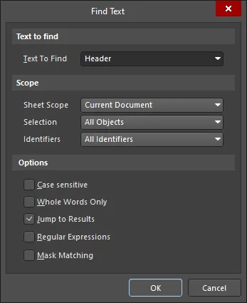
テキスト検索 回路図および回路図シンボルエディタでは、定義された検索オプションに従って、特定のテキストや部分的なテキストを素早く検索することができます。メインメニューから Edit " Find Text コマンドを選択するか、デザインスペース内で右クリックしてコンテキストメニューから Find Text コマンドを選択するか、 Ctrl+F キーボードショートカットを使用して Find Text ダイアログにアクセスします。このダイアログを使用して、検索する既存のテキストを、スコープや追加オプションとともに指定します。
テキストの検索 ダイアログ
テキストの検索ダイアログのオプションとコントロール
検索するテキスト 検索するテキスト - このフィールドを使って検索するテキスト文字列を入力します。完全な単語を入力するか、部分的な文字列を検索します。後者の場合、 Whole Words Only オプションを無効にする必要があります。文字列にはワイルドカード文字 ?(1文字) および * (任意の文字グループ) を含むことができます。 ワイルドカードは常に大文字と小文字を区別しません。
検索された各文字列は、素早く検索できるようにフィールドのドロップダウンリストに追加されます。
Scope Sheet Scope - このフィールドを使用して、関連する回路図ドキュメントのテキスト検索の範囲を決定します。 Current Document - アクティブなドキュメントのみを検索します。 Project Documents - アクティブなプロジェクト内のすべての回路図ドキュメントを検索します。 Open Documents - 所属プロジェクトに関係なく、開いているすべての回路図ドキュメントを検索します。 Project Physical Documents - アクティブなプロジェクトのソース回路図ドキュメントの Compiled Document タブビューを検索します。 Project Physical Documents を横断してテキストを検索するには、アクティブなプロジェクトを最初にコンパイルする必要があります。これを行わないと、検索は論理シート( Editor ドキュメントのタブビュー)のみで行われます。
Selection - このフィールドを使用すると、オブジェクトの現在の選択状態に基づいて、検索の範囲をさらに制限することができます。以下のオプションから選択します:
Selected Objects - 検索対象を、現在選択されているオブジェクトのみに制限します。 DeSelected Objects - 検索対象を、現在選択解除されているオブジェクトのみに制限します。 All Objects - 制限なし。選択状態に関係なく、すべてのオブジェクトを検索します。 Identifiers - このフィールドを使用して、テキストベースのオブジェクトのタイプに基づいて検索範囲をさらに制限します。以下のオプションから選択してください:
All Identifiers - 制限なし。すべてのテキスト・ベース・オブジェクト(テキスト文字列、テキスト・フレーム、ピン、ネット識別子、およびデジグネータ)を検索します。 Net Identifiers Only - 検索対象をネット識別子(ポート、パワー・ポート、シート・エントリ、オフ・シート・コネクタ、およびネット・ラベル)のみに制限します。Designators Only - 検索対象をコンポーネント・デジグネータのみに限定します。 Options Case sensitive - このオプションを有効にすると、大文字と小文字を区別して検索を実行します。つまり、ターゲット・テキストは、 Text To Find フィールドに入力された検索テキストの大文字と小文字に一致する必要があります。
Whole Words Only - このオプションを有効にすると、検索対象が単語全体に限定されます。これは、検索テキストがそのまま完全に存在し、より大きなテキスト文字列の一部であってはならないことを意味します。例えば、このオプションを有効にすると、"cat "を検索する場合、"category "の最初の3文字は有効な検索対象とはみなされません。部分文字列を自由に検索するには、このオプションを無効にします。
Jump to Results - このオプションを有効にすると、一致/検索されたテキストがズームされ、デザインスペースの中央に表示されます(可能な場合)。検索で複数の一致が得られた場合、 Find Text - Jump ダイアログが開きます。このダイアログを使用して、一致した検索結果間をジャンプします。
正規表現 - 正規表現を使用して検索する場合はチェックしてください。
- 文字列が行頭にある場合のみマッチします。 $ - 文字列が行末にある場合のみマッチします。 . - 任意の1文字を示します(例、"te.t "は、"test"、"text"、および "tent "にマッチするが、"tet "にはマッチしない)。 * - 文字なしを含む、任意の文字のセットを示す(たとえば、"te*"は、"text"、"tent"、および "te "にマッチするが、"t "にはマッチしない)、"te+" は、"text"、"tent "にマッチするが、"te "にはマッチしない)。 [ ] - 大括弧で囲まれた文字のいずれかを見つける。 [^] - 大括弧で囲まれた文字列の先頭にあるカレットは、NOTを意味する(例、"[^tes]"は、t、e、s以外の文字にマッチします)。 [-] - 大括弧内の文字列内のハイフンは、文字の範囲を意味します(例えば、"[l-o]"は、l、m、n、oの文字にマッチします)。 { } - 文字や式をグループ化するために使用されます。 - ワイルドカード文字の前にバックスラッシュを付けると、回路図エディタまたは回路図ライブラ リ・エディタがその文字をワイルドカードとしてではなく、文字通りに扱うように指示します(例 えば、" \^test" はワイルドカードとして扱われません)、「 Mask Matching - このオプションを有効にすると、 Jump to Results オプションが有効になっているときに、 Preferences ダイアログの System - Navigation page の設定に従って、マッチング・テキストがデザイン空間で拡大または縮小されます。
すべての一致するテキストが Messages パネルにリスト表示され、検索されたテキストのインスタンスにデザインスペース内で直接クロスプローブできます(メッセージエントリをダブルクリックするか、右クリックしてコンテキストメニューから Cross Probe を選択)。さらに、 Find Text ダイアログで、 Jump to Results オプションが有効になっており、検索するテキストの複数のインスタンスが返された場合、 Find Text - Jump ダイアログが表示され、 Find Text ダイアログの Text To Find フィールドで指定されたテキストの最初の出現位置がデザインスペース内の中央に表示されます。
Find Text - Jump ダイアログ
Find Text - Jump ダイアログは、非モーダルダイアログです。ダイアログを開いている間、回路図シート上のオブジェクトを含む Altium Designer のインターフェイスを操作できます。
テキスト検索 - ジャンプダイアログのオプションとコントロール
前へ - このボタンをクリックすると、前の一致するテキスト項目が表示されます。繰り返しクリックすると、順次項目を遡ります。
次へ - このボタンをクリックすると、次に一致するテキスト項目が表示されます。繰り返しクリックすると、項目が順次前に進みます。
検索されたテキストに一致する項目を前後にステップすると、ダイアログの上部には、元の検索テキストと、オブジェクトのタイプ(デジグネータ、ネット識別子、ポート、電源ポート、ネット・ラベル)、テキスト文字列、またはテキスト・フレーム)とその一致するテキストという点で、デザイン・スペースに表示されている現在の項目が反映されます。
Close - ダイアログを閉じるには、このボタンをクリックします。ボタンの右側にあるドロップダウン矢印をクリックすると、以下のオプションを含むメニューにアクセスできます:
New Search - このコマンドを選択するとダイアログが閉じ、 Find Text ダイアログが開きます。ここから必要に応じて検索内容を変更することができます。 Close - このコマンドを選択するとダイアログが閉じ、デザインスペースに戻ります。または、 Esc キーボードショートカットを使用してこの操作を実行します。
検索されたテキストの別の結果にジャンプします:
[Find Text - Jump] ダイアログの [Previous] および [Next] ボタンを使用します。
Edit " Find Next コマンドを使用する( F3 ショートカットを使用する)。
メッセージ パネルの対応するメッセージエントリからクロスプローブする。
定義された検索オプションに従って特定のテキストまたは部分的なテキストを検索し、そのテキストを指定の新しいテキストに置き換えることもできます。メインメニューから Edit " Replace Text コマンドを選択するか、 Ctrl+H キーボードショートカットを使用して、 Find And Replace Text ダイアログにアクセスします。このダイアログを使用して、検索する既存のテキストと、使用する置換テキストを、スコープや追加オプションとともに指定します。準備ができたら、 OK をクリックします。 Prompt On Replace オプションがダイアログで有効になっていない限り、すべてのターゲット テキストが置換されます。
テキストの検索と置換 ダイアログ
テキストの検索と置換ダイアログのオプションとコントロール
テキスト 検索するテキスト - このフィールドを使用して、検索するテキスト文字列を入力します。完全な単語を入力するか、部分的な文字列を検索します。後者の場合、 Whole Words Only オプションを無効にする必要があります。文字列にはワイルドカード文字 ?(1文字) および * (任意の文字グループ) を含むことができます。 ワイルドカードは常に大文字と小文字を区別しません。
検索された各文字列は、フィールドのドロップダウンリストに追加され、素早く検索できるようになります。
Replace With - このフィールドを使用して置換テキスト文字列を入力します。入力されたテキストは、 Text To Find の入力および定義されたオプションによって検索された結果のテキスト文字列を完全に置き換えます。
選択的文字列置換は、 {oldtext=newtext} 構文を使用して、検索文字列の一部だけを変更することができます。例えば、文字列 VCC を Text to Find フィールドに入力し、文字列 {CC=DD} を Replace With フィールドに入力すると、文字列 VCC のすべてのインスタンスが VDD に変更されます。一番左の括弧で囲まれた置換が最初に行われ、次に右の括弧で囲まれた置換が行われる、といった具合です。
Scope Sheet Scope - このフィールドを使用して、関連する回路図ドキュメントのテキスト検索の範囲を決定します。 Current Document - アクティブなドキュメントのみを検索します。 Project Documents - アクティブなプロジェクト内のすべての回路図ドキュメントを検索します。 Open Documents - プロジェクトを問わず、開いているすべての回路図ドキュメントを検索します。 Selection - このフィールドを使用して、オブジェクトの現在の選択状態に基づいて、検索範囲をさらに制限します。以下のオプションから選択してください:
Selected Objects - 検索対象を、現在選択されているオブジェクトのみに制限します。 DeSelected Objects - 検索対象を、現在選択解除されているオブジェクトのみに制限します。 All Objects - 制限なし。選択状態に関係なく、すべてのオブジェクトを検索します。 Identifiers - このフィールドを使用して、テキストベースのオブジェクトのタイプに基づいて、検索範囲をさらに制限します。以下のオプションから選択してください:
All Identifiers - 制限なし。すべてのテキスト・ベース・オブジェクト(テキスト文字列、テキスト・フレーム、ピン、ネット識別子、およびデジグネータ)を検索します。 Net Identifiers Only - 検索対象をネット識別子(ポート、パワー・ポート、シート・エントリ、オフ・シート・コネクタ、およびネット・ラベル)のみに制限します。Designators Only - 検索対象をコンポーネント・デジグネータのみに限定します。 Options Case sensitive - このオプションを有効にすると、大文字と小文字を区別して検索を実行します。つまり、ターゲット・テキストは、 Text To Find フィールドに入力された検索テキストの大文字と小文字に一致する必要があります。このオプションは置換テキストには関係なく、単に Replace With フィールドに入力されたテキストに使用された大文字小文字に従います。
Prompt On Replace - このオプションを有効にすると、一致するテキストの各インスタンスの置換を手動で確認するようプロンプトが表示されます。 Confirm ダイアログを使用して各インスタンスを順番に処理し、最後に Information ダイアログで置換の回数を要約します。こ のオプシ ョ ン を無効にす る と 、 検索テ キ ス ト に一致す る すべての イ ン ス タ ン ス が、 手動での確認な し に置換 さ れます。同様に、 情報 ダイアログが表示され、置換された数が表示されます。
Whole Words Only - このオプションを有効にすると、検索対象が単語全体に限定されます。これは、検索テキストがそのまま完全に存在し、より大きなテキスト文字列の一部であってはならないことを意味します。例えば、このオプションを有効にすると、"cat "を検索する際、"category "の最初の3文字は有効な検索対象とはみなされません。部分文字列を自由に検索するには、このオプションを無効にします。
正規表現 - 正規表現を使って検索する場合にチェックする。
- 文字列が行頭にある場合のみマッチする。 $ - 文字列が行末にある場合のみマッチする。 . - 任意の1文字を示す(例、"te.t "は、"test"、"text"、および "tent "にマッチするが、"tet "にはマッチしない)。 * - 文字なしを含む、任意の文字のセットを示す(たとえば、"te*"は、"text"、"tent"、および "te "にマッチするが、"t "にはマッチしない)、"te+" は、"text"、"tent "にマッチするが、"te "にはマッチしない)。 [ ] - 大括弧で囲まれた文字のいずれかを見つける。 [^] - 大括弧で囲まれた文字列の先頭にあるカレットは、NOTを意味する(例、"[^tes]"は、t、e、s以外の文字にマッチします)。 [-] - 大括弧内の文字列内のハイフンは、文字の範囲を意味します(例えば、"[l-o]"は、l、m、n、oの文字にマッチします)。 { } - 文字や式をグループ化するために使用されます。 - ワイルドカード文字の前にバックスラッシュを付けると、Schematic EditorまたはSchematic Library Editorはその文字をワイルドカードとしてではなく、文字通りに扱うようになります(例えば、"˶^test "は行頭の文字列testを探すのではなく、文字列"^test "を探します)。
検索できるのは、回路図ドキュメント内または回路図ライブラリドキュメント間のみで、2つのドキュメントタイプを組み合わせて検索することはできません。
ユニオンの操作 ユニオンはグループ化されたオブジェクトの集まりです。ユニオンとしてグループ化されている場合、すべてのユニオンメンバーを素早く選択/選択解除することができ、ユニオンのメンバーを1つ移動させると、それらすべてを移動させることができます。
現在選択されているデザインオブジェクトからユニオンを作成するには、メインメニューから Tools " Convert " Create Union from selected objects コマンドを選択するか、デザインスペース内で右クリックし、コンテキストメニューから Unions " Create Union from selected objects コマンドを選択します。選択したオブジェクトをメンバーとするユニオンが作成されます。情報ダイアログが表示され、ユニオンに追加されたオブジェクトの数が確認できます。
ユニオンに含まれる全てのオブジェクトを移動する基本的な方法は、ユニオンのメンバーオブジェクトをクリックしたままカーソルをドラッグし、ユニオンに含まれる全てのオブジェクトを移動することです。しかし、回路図エディタでは、電気オブジェクト(コンポーネント、ワイヤ、ポートなど)のドラッグもサポートしており、この機能が有効になっている場合、電気オブジェクトをドラッグしようとすると、ユニオンの移動が優先され、オーバーライドされます。
コンポーネントなどの電気オブジェクトをドラッグするには、 Preferences ダイアログの Schematic - Graphical Editing ページ で、 Always Drag オプションを有効にします。このオプションを有効にすると、電気的オブジェクトをクリックしてドラッグしたときに、現在の接続を維持し、ドラッグに合わせて配線をきれいに調整するようにソフトウェアに要求します。
Always Drag オプションの現在の状態は、 Ctrl キーを押しながら作業することで、一時的に切り替えることができます。 Always Drag オプションが有効で、 Ctrl + クリック、ホールド、ドラッグすると、ソフトウェアは接続を維持しようとせず、代わりにカーソル下のオブジェクトを移動します。この場合、そのオブジェクトがユニオンのメンバーであれば、ユニオン内のすべてのオブジェクトが移動します。 Always Drag を有効にして作業する場合は、 Ctrl を押しながらクリック&ドラッグすると、ユニオン内のすべてのオブジェクトが移動します。 Always Drag が無効になっている場合、 Ctrl を押すと、オブジェクトの移動からドラッグに切り替わります。
現在カーソルの下にあるオブジェクトがメンバーであるユニオンのすべてのオブジェクトを選択/選択解除するには、必要なユニオンのメンバーであるオブジェクトの上で右クリックし、コンテキストメニューから Unions " Select All In Union / Deselect All In Union コマンドを選択します。


-
-
-


特定のユニオンから1つ以上のメンバーオブジェクトを削除するには、メインメニューからTools " Convert " Break objects from Union コマンドを選択します。コマンドを起動すると、カーソルが十字に変わり、ユニオンから削除するオブジェクトを選択するように指示されます。カーソルを必要なメンバーオブジェクトの上に置いてクリックするか、Enter を押します。Confirm Break Objects Union ダイアログが表示されます。このダイアログを使用して、どのオブジェクトをユニオンから削除するか(逆に、どのオブジェクトをそのユニオンの一部として残すか)を決定します。OK をクリックすると、それに応じてユニオンのオブジェクト・メンバーシップが更新されます。
![[Confirm Break Objects Union] ダイアログ](https://files.doc.altium.com/sites/default/files/wiki_attachments/320767/Confirm_Break_Objects_Union_SCH_AD18.webp "[Confirm Break Objects Union] ダイアログ")
[Confirm Break Objects Union] ダイアログ
Confirm Break Objects Union ダイアログのオプションとコントロール
[Choose Objects to Keep or Remove from Union]
-
[Object Kind] - オブジェクトの種類(ネットラベル、バス、ハイパーリンクなど)を表示します。
-
Description - オブジェクトの説明(高さ/幅、デジグネータなど)を表示します。
-
Keep in Union - ユニオンから削除するオブジェクトをマークします。
-
All On - クリックするとすべてのオブジェクトがユニオンから削除されます。
-
All Off - クリックするとすべてのオブジェクトの選択が解除されます。
あるいは、必要なユニオンのオブジェクトの上で右クリックし、コンテキストメニューからUnions " Break objects from Union コマンドを選択することで、親ユニオンからオブジェクトを削除できます。
現在の回路図ドキュメントに定義されている全てのユニオンを解除(解散)するには、メインメニューからTools " Convert " Break all objects Unions コマンドを選択します。デザイン内の全てのユニオンは解消され、グループ化されていたオブジェクトは残りません。情報ダイアログで、いくつのオブジェクトが、いくつのユニオンから削除されたかが確認できます。

 AI で翻訳