Parent page: Capturing the Logical System Design
The connections established between modules in the schematic ultimately represent the connectivity between child project connectors, connector pins, and nets in the overall system design. The multi-board schematic editing environment provides comprehensive features that may be used to define, modify, check and update that connectivity as the overall product design is developed.
Connecting Child projects
To complete the process of creating and connecting Child Project Modules together, place a logical Connection between the Module Entries.
A range of connection types is available from the editor's Place menu or the Active Bar (at the top of the workspace), including Direct Connection and Wire, which refer to connectors that plug together or are wired together, respectively. Click and drag the connection line between the Module Entry points to create the logical connectivity. Note that all elements in the system schematic editor, including Entry objects, can be dragged to a new location.
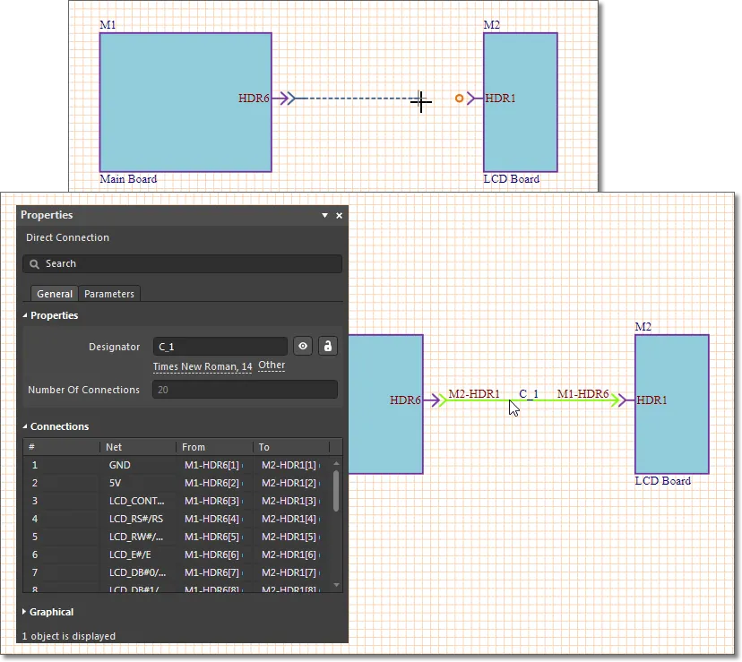
Select a
Connection graphic in the workspace to see its details, such as the included Nets and Pin connections, in the
Properties panel.
Connection
 A placed Wire type Connection between Module Entries.
Summary
A Connection is a graphical object that is placed between Module Entries in a multi-board Design document to interconnect Modules. Multi-board Connections represent the physical connections (wires, plugs and sockets, cables, or harnesses) that are used between the child board designs.
Types of Connections
The Multi-board system editor offers two broad types of Connections that can be placed between Module Entries:
- Simple – the connection between the Module Entries is through a collection of wires, or as a direct PCB plug-in via mated connectors.
- Wire – the connection is represented as individual wires between the pins of each Module Entry connector.
- Direct Connection – the connection is represented as a direct mating between the pins of each Module Entry connector.
- Grouped – the connection between Module Entries is through a collected set of Nets that are terminated by a physical connector part (plug, socket, header, etc.,) at each end.
- Cable – the connection is represented by a physical cable with terminating connectors that mate to the (board) connectors at each Module Entry.
- Harness – the connection is represented by a physical harness with terminating connectors that mate to the (board) connectors at each Module Entry.
Availability
Connections are available for placement in the multi-board schematic editor as follows:
- Choose the Place » <connection type> command from the main menus, where connection type is a Wire, Direct Connection, Cable, or Harness.
- Select a Connection type on the Active Bar located at the top of the design space. Click and hold an Active Bar button to access other connection commands.
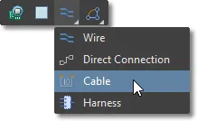
- Right-click in the drawing design space then select Place » <connection type> from the context menu.
Placement
After launching the command, the cursor will change to a cross-hair, indicating connection placement mode. For all types of Connections, placement is made by performing the following actions:
- Hover the cursor over a Module Entry's connection indicator (orange circle), which will change to a green circle to indicate a valid connection point.
- Click to confirm the Connection line's starting point.
- Reposition the cursor then click to place a series of vertex points that define the path of the wire.
- Position the cursor over the destination Module Entry connection point then click to complete the Connection line path.
- Continue placing further Connections between other Module Entry pairs, or right-click or press Esc to exit placement mode.
After Placement
After placing a Connection, the individual connections within it can be examined in the Properties panel. To edit the individual connections within a Connection, use the Connection Manager (Design » Connection Manager). Changes made in the Connection Manager can be pushed back to the child PCB projects, using the Design » Update Child Projects command.
Note that there is an additional step required if the Connection type is Cable or Harness. These Connection types must have a cable/harness connector component assigned before the individual connections will appear in the Properties panel or the Connection Manager. The cable/harness connectors are assigned in the Properties panel, as shown below.
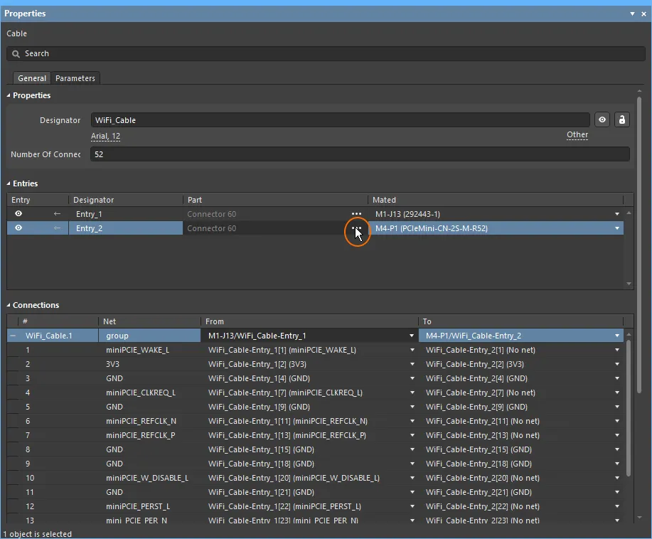
- Cable and Harness connectors are assigned in the Multi-board schematic editor and can be included in the Multi-board Bill of Materials.
- The other elements that make up the cable or harness assembly cannot be included on the Multi-board schematic, but can be included directly in the BomDoc by creating Manual Solutions in ActiveBOM.
- Alternatively, there are resources available that demonstrate how cable design can be achieved in the schematic editor. For example, this video created by the team at Nine Dot Connects shows how to create the elements in a cable and design the cable in the schematic editor.
Graphical Editing
This method of editing allows a placed Connection object to be selected in the design space and graphically edit its path or terminating points.
Once selected, a Connection line is highlighted (green) and can be manipulated as follows:
- Click and drag a line segment in its perpendicular plane to alter the connection line path.
- Click and drag a Connection terminating point (at a Module Entry) to reposition its location, then click to confirm. Normally, the connection end would be moved to another Module Entry, but it also can be positioned in free space where it adopts a nominal end point identifier.
 A selected Wire Connection being graphically manipulated.
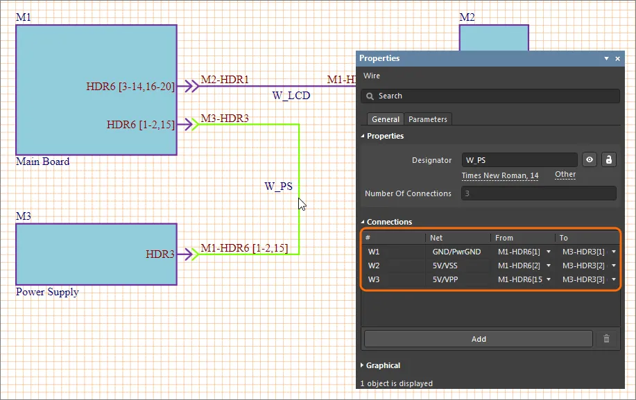
A placed and terminated Connection is automatically assigned a Designator (W_PS in the example above) as an object identifier, which is editable in the Properties panel. Its terminating ends are identified by their connection target information in the format <TargetModuleDesignator>-<TargetEntryDesignator>.
Non-Graphical Editing
Properties page: Connection Properties
The non-graphical method of editing a Connection is available in the multi-board Properties panel, which provides editable property fields for the item that is currently selected in the design space.
 The Properties panel when a Wire Connection object is selected.
To open the Properties panel and access the properties of a placed Connection:
- After selecting the Connection object, select the Properties panel from the Panels button at the bottom right of the design space or select View » Panels » Properties from the main menus.
- Double-click on the Connection object.
- Right-click on the Connection then select Item Properties from the context menu.
If the Properties panel is already active, click on the Connection to access its properties in the panel.
The Connection properties can be accessed prior to entering placement mode, from the
Multi-board Schematic – Defaults page of the
Preferences dialog. This allows the default properties for the Connection object to be changed, which will be applied when placing subsequent Connections.
Editing Multiple Objects
The Properties panel supports multiple object editing where the property settings that are identical in all currently selected objects may be modified. When multiples of the same object type are selected, a Properties panel field entry can be edited for all selected objects. If values of a property are different for objects in the selection, the appropriate field will be shown as an asterisk (*); a new property value will be applied to all selected objects.
Connection Properties
Multi-board object properties are definable options that specify the visual style, content and behavior of the placed object. The property settings for each type of object are defined in two different ways:
- Pre-placement settings – most Connection object properties, or those that can logically be pre-defined, are available as editable default settings on the Multi-board Schematic - Defaults page of the Preferences dialog (access from the
 button at the top-right of the design space). Select the object in the Primitive List to reveal its options on the right.
- Post-placement settings – all Connection object properties are available for editing in the Properties panel when a placed Connection is selected in the design space.
 mode of the Properties panel") The Cable Connection object default settings in the Preferences dialog and the Wire (Connection) mode of the Properties panel
The Cable Connection object default settings in the Preferences dialog and the Wire (Connection) mode of the Properties panel
A Connection is the general term used for the four types of physical interconnections that may be applied between child board designs (modules) in multi-board schematic documents. The Connection types are Cable, Direct, Harness, and Wire.
In the below properties listing, options that are not available as default settings in the Preferences dialog are noted as; 'Properties panel only'.
Properties
- Designator – specifies the schematic identifier for this Connection.
- Use the
 button to toggle its visibility in the schematic and the
  button to toggle the value's ability to be edited.
- Select the font link to access and edit the Designator's font settings, attributes and color. Select the Other link to set auto-positioning (Designator centrally alongside the Connection line).
- Number of Connections (Properties panel only) – reports the number of individual connections in the currently selected Connection.
Entries (Properties panel only)
This region is available for Cable and Harness type connections only.
The Entries section defines the physical attributes for each terminating end of a Cable/Harness connection.
- Entry column – sets the Designator visibility () and style (male/female) for the Connection end.
- Designator column – specifies the schematic identifier for the Connection end point.
- Part column – the specified physical part (component) used for terminating the Connector end. Click the
 button browse to and select a suitable Library component part, such as a plug, socket, header, etc.
- Mated column – the connection on the target board design (represented by a Module Entry) to which the Cable or Harness end is mated. The associated drop-down list offers other available connection targets – generally, that occupied by the other connection end.
Connections (Properties panel only)
The Connections section is a tabular list of the individual, mapped Net connections within the placed Connection, including their Module Entry terminating points.
For simpler type Connections such as a Wire or Direct Connection, the available fields are as follows:
- # (number) column – the designated number assigned to the individual Wire/Pin in the parent Connection.
- Net column – the net name assigned to the connection in an aggregated form that combines the From and To Net names at their respective Module Entries.
- From column – the registered details of one terminating end of the individual connection, which includes the parent Module, Module Entry, Pin/Wire number, and Net.
- To column – the registered details of the other terminating end of the individual connection, which includes the parent Module, Module Entry, Pin/Wire number, and Net.
For grouped type Connections such as a Cable or Harness, the available fields are as follows:
- # (number) column – the designated number assigned to the Cable or Harness based on its Designator.
- Net column – set to
group for this type of Connection indicating that a collection (group) of pin-to-pin Net connections are hosted by the parent Connection.
- From column – the registered details of one terminating end of the connection based the Module Entry name and the Cable/Harness and Entry designators (see Entries above).
- To column – the registered details of the other terminating end of the connection based the Module Entry name, and the Cable/Harness and Entry designators (see Entries above).
Graphical
- Line – displays the current Connection line pattern style and color.
- Line pattern – the pattern style applied to the Connection line. Use the drop-down -to choose from a range of line style presets.
- Line color (
 ) – click to open the outline color selector drop-down, which includes options for preset colors, HEX/RGB color values and the graphic selection of color shades.
Parameters tab (Properties panel only)
Parameters that are associated with a Connection are accessed under the Parameters tab of the Properties panel. All other properties are accessed under the default General tab.
- Name – the Parameter Name of the listed parameter entry.
- Value – the Parameter Value associated with the listed parameter Name.
- Options
- Use the button to toggle a Parameter's visibility in the schematic and the button to toggle its ability to be edited.
- Select the font link to access and edit the Parameter's font settings, attributes and color. Select the Other option to set auto-positioning (Parameter at the bottom of the Connection rectangle), and the visibility of the Parameter Name.
- Add/Delete – click
 to add a new default Parameter entry to the list. Click
  to remove the selected Parameter from the list.
Split Connections
In design situations where a child project connector serves more than one connected project, the source connector can be logically divided (in terms of pins/nets) using the multi-board schematic editor’s Split feature – in practice, one module is connected to two other modules.
An example of such a design would be where a single header plug on a PCB is intended to accommodate two smaller header sockets, which, in turn, connect to two other PCBs – the sectioned signals from a single (e.g., 20-pin) connection are distributed to a (e.g., 10-pin) connection one PCB and a (10-pin) connection on another PCB.
To split a connection, select the Module and then an Entry in the Properties panel. Select the  button, and in the subsequent Split Entry dialog, check the listed pin Pin/Net combinations you want to separate (split off) to another Entry. Use the
  button to confirm the selections.
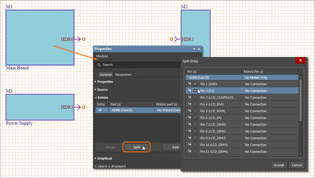
The editor will automatically create a new Module Entry for the separated Pins/Nets, which can then be connected to a different Module as required.
In the example shown, Entry HDR6 on Module M1 is intended to connect to both Module M2 (a panel LCD display) and Module M3 (a power supply board). The HDR6 Entry connections have been split to logically separate out three power Nets that will connect to HDR3 on power supply Module M3. This creates an additional HDR6 Entry on M1 (HDR6 [1-2,15]) that offers just the three power connections for M3, while the original HDR6 Entry is automatically reassigned to offer the remaining 17 connections, which ultimately connect to HDR1 on the LCD Module M2.
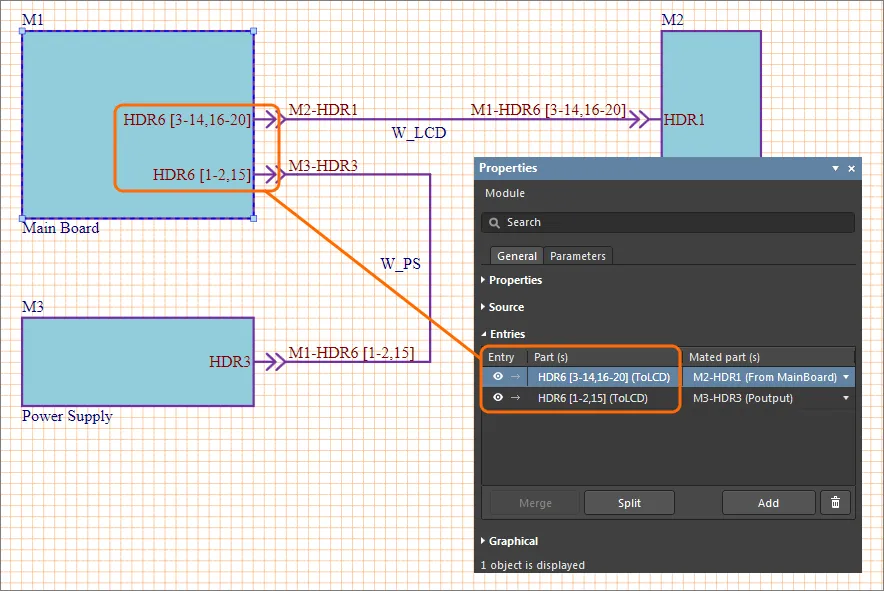
Select a Connection in the workspace to see its constituent Nets in the Properties panel. Here, one section of the (split) HDR6 Nets is connected to HDR3 through the wire connection W-PS, which represents the three power lines between the Main Board (M1) and Power Supply (M3). As shown in the image below, each virtual wire listed in the panel’s Connections area also includes its Entry name, Pin and Net at either end in the From and To columns.
Note that along with a connection's Designator, the wire name (#) and local Net name (Net) for each entry in the Connections list can be edited for convenience. These names are local to the Multi-board system design and do not affect the source Child Projects.
Edit Connections
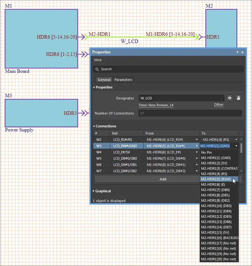
The connections between Child Project Modules are not necessarily a pin-to-pin match, particularly when a connector is split in sections that are wired to different PCB Modules.
To edit or correct the Pin/Net matches between a Module interconnection, select the Connection in the workspace and then change the From/To assignments as required in the Properties panel’s Connections list entries.
Use the From or To drop-down list to select a new Net assignment, and therefore a different end-to-end signal relationship through that individual connection or wire, within the Module-to-Module connection.
Connection Manager
The overall connectivity in a Multi-board design, once established, is detailed in the Connection Manager dialog (Design » Connection Manager).
This dialog lists all Net/Pin assignments grouped under their parent Connection Designators and type (Wire, Direct, etc.,), and includes their system design ID and Net Name, along with their From and To Pin/Net connections. Use the dialog’s  option to include details of the literal Pin connections in the listing.
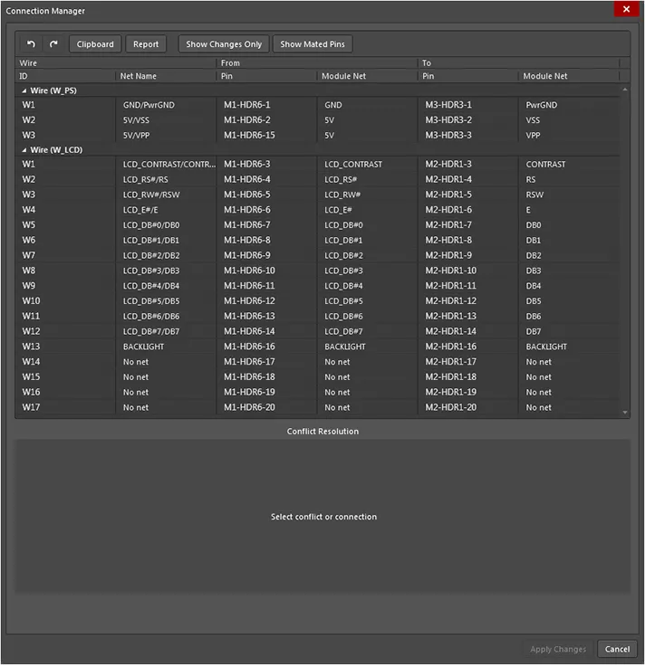
The dialog’s lower Conflict Resolution area will indicate any connection conflicts between the current Multi-board system design and source (child) projects during a design update, as outlined below.
