
Importing a Design from OrCAD
Translating complete OrCAD® designs, including Capture™ schematics, Layout™ PCB files, and library files can all be handled by Altium Designer's Import Wizard (to OrCAD version 17.4). The Import Wizard removes much of the headache normally found with design translation by analyzing the imported files and offering defaults and suggested settings for the project structure, layer mapping, PCB footprint naming, and more. The flexibility provided through the Wizard steps gives you as little or as much control as you like over the file translation settings before committing to the actual translation process.
Importing OrCAD Files
The OrCAD design file importer is available through Altium Designer's Import Wizard (File » Import Wizard) by selecting the Orcad Designs and Libraries Files option on the Wizard's Select Type of Files to Import page. The Wizard provides options for nominating both schematic/pcb design files and library files, and also OrCAD to Altium Designer PCB layer mapping options.

Import Wizard - Orcad Designs and Libraries Files
Orcad Designs and Libraries Files

Importing Orcad Designs

Click Add to choose which OrCAD design files to include in the import process. You can delete a selected file by clicking Remove.
Importing Orcad Libraries

Click Add to choose which OrCAD library files to include in the import process. You can delete a selected file by clicking Remove.
Reporting Options

Use the Reporting Options page to set up general log reporting options.
Under General Settings, enable the desired options: Log All Errors, Log All Warnings, and Log All Events.
Schematics General Options

Use this page of the Wizard to control how OrCAD objects are imported.
Enable Convert Orcad Component Rectangles to Altium Designer Rectangles if desired.
Enable Convert Orcad Off-Page connectors as Altium Ports (instead of defaults Off-sheet connectors) if desired.
Schematics Sheet Options

Use this page of the Wizard to control how OrCAD pages are imported.
Title Blocks – OrCAD title blocks are imported as schematic components. In Altium Designer, title blocks are limited to two types: Standard and ANSI, and the graphics for them are not editable. Templates can be used if you desire a more flexible solution. Templates allow any graphical data to be placed onto a schematic sheet.
- Strip Orcad Title Blocks – enable to strip the OrCAD title blocks.
-
Enable AdvSCH Title Blocks – check to enable AdvSCH title blocks. Use the drop-down to select
StandardorANSI.
Pin-to-Pin Spacing
- Pin-to-Pin Spacing – enter the desired spacing ratio.
- Resize Sheet – enable to resize the sheet based on the pin-to-pin spacing entered in the above textbox.
Schematics Parameter and Net Connectivity Options

Use this page of the Wizard to control how OrCAD properties and junctions are imported.
Properties – OrCAD properties are generally imported as schematic parameters, with the exception of wire properties, which are imported as texts.
- Auto-position Parameter – enable to automatically place schematic parameters out of the way after rotation or other movements.
- Disable "Mark Manual Parameters" – manually-positioned parameters will be marked with blue dots. Check this box to disable this feature.
- Force convert all I/O and Bi-directional pins to passive pins - enable to force all I/O and bi-directional pins to be converted to passive pins.
-
Import Orcad Junctions – use the drop-down to select which junctions to import. Choices include:
Only Cross JunctionsandAll.
PCB Color and Rules Options

Options
- Run Online DRC after importing files – use the drop-down to select between Suppress Online DRC and Use Preference Settings, depending on how you'd like the DRC run after importing files.
- Use Orcad Color Settings – enable to use imported Orcad Color settings.
Design Rules
- Import Solder Mask Rules – enable to import Orcad Solder Mask rules.
- Import Solder Paste Rules – enable to import Orcad Solder Paste rules.
- Allow Via Underneath Pad – enable to allow imported vias underneath pads.
- Import Free Vias As Vias – enable to allow imported free vias as vias.
Current PCB Layer Mappings

This page of the Wizard is used to review and edit the layer mapping for each Orcad PCB. Default mapping is provided by the Wizard to build the layer mapping for each PCB. Layer mapping can be customized for each of your designs to be imported. You may wish to import multiple Orcad PCB designs and map the same Orcad layer to the same Altium Designer layer. You can set your layer mapping once and use this layer mapping for all of your files to be imported. The advantage of importing in this manner is that batch layer management can save time when importing multiple designs. The disadvantage to using this is that Default Layer Mapping is not always intelligent with differing structures in designs, and therefore, some manual changes may be required.
The Orcad Layer Name, Orcad Layer Type, and Altium Design Layer are listed in the grid region. Click on the ![]() icon on the right-hand side of each region to filter the displayed list of that region.
icon on the right-hand side of each region to filter the displayed list of that region.
If desired, you can edit the layer mapping for any or all Orcad Import PCB designs or library files on this page of the Wizard. To group by a column, drag the column header into the area at the top of the table specified.
- File Menu – use this option to jump to the file path entry.
Right-clicking in the grid region or selecting the Menu button provides you with a sub-menu where you can:
-
Invert Selection – select to invert the items that are selected to not selected, and those that are not selected to selected.
-
Set Selection To – select to access a sub-menu of layer types (listed below) with their own sub-menus of layers from which you can choose the desired layer:
-
Signal Layers -
Plane Layers -
Mechanical Layers -
Other Layers
-
-
Load Layer Mapping – select to open the Load Configuration dialog to load the desired mapping files.
-
Save Layer Mapping – select to open the Choose File to Save Layer Mapping dialog. Choose a file from the File Paths list that you'd like to save as a Layer Mapping File (*.lni). Once selected, choose OK to open the Save Configuration dialog, where you may determine where you'd like to save the file.

The Choose File to Save Layer Mapping dialog
Output Library Options

Use this page of the Wizard to control how the imported libraries are grouped.
Library Import Options – select one of the following options for how to group output libraries.
- Output Libraries as PCB Project – select to minimize the integration between PCB and schematic libraries. The imported libraries will only be grouped as a PCB project. They can be added to the list of libraries in the library panel later. This setup is most advantageous for those who wish to operate in the same environment as they did in OrCAD.
- Output Libraries as Library Packages – select to group the libraries into library packages. You can then select to compile the library packages as integrated libraries by enabling Compile as Integrated Libraries. Integrated libraries combine both PCB, schematic and PSpice libraries, enabling better interactions. Errors in the compilation are shown in the Messages panel.
Placement Outline Obstacles

- Convert Orcad Placement Outline Obstacles – enable if you wish to convert Orcad placement outline obstacles.
- Altium Designer Layer – use this field to determine which mechanical layer you'd like to override.
- Outline track width – use this field to enter the desired outline track width.
Output PCB Projects

Use this page of the Wizard to review the output project structure and specify the output directory in which to import the files. Use the Browse Folder icon to search for and choose the Project Output Directory.
Click Menu to access options to edit the project structure:
-
Create Project – click to open the Create Project dialog to add a project.

Use the Create Project dialog to add a new project. -
Rename Project – click to rename the selected project. This option is available only when a
*.PrjPcb fileis selected. - Remove Selected Projects – click to remove the selected project from the PCB Projects structure.
- Reset Structure to Default – click to reset the PCB Projects structure to the defaults.
-
Add Designs to Project – click to add a design(s) to the project. This option is available only when a
*.PrjPcb fileis selected. - Remove Selected Designs - click to remove the selected design files.
Output Libraries

The output directory for the imported libraries are shown on this page of the Wizard. Use the Browse Folder icon to search for and choose the desired Library Output Directory.
Executing Import Process
A green progress bar shows the progress of the import process while also listing each file at the process continues.
Closing the Wizard

The OrCAD Import Wizard has completed. The Messages panel appears with any relevant messages. Click Finish to close the Wizard. If any warnings were generated during the import process, a *.LOG file opens showing the warnings.
Imported OrCAD files translate as follows:
-
OrCAD Layout (
*.MAX) files translate to Altium Designer PCB files (*.PcbDoc). -
OrCAD Capture (
*.DSN) files translate to Altium Designer schematic files. Each page within a.DSNfile will be imported as a single Altium Designer schematic file (*.SchDoc). Design caches within a.DSNfile will be imported as a schematic library (*.SchLib). Design hierarchy is maintained, including complex hierarchy. -
OrCAD .OLB (schematic library) files will be translated into Altium Designer schematic library files (
*.SchLib). -
OrCAD .LLB (PCB library) files will be translated into Altium Designer PCB library files (
*.PcbLib). -
Translated OrCAD libraries are automatically grouped into one PCB project.
File Translation
Imported OrCAD files translate as follows:
- OrCAD Layout (*.MAX) files translate to Altium Designer PCB files (*.PcbDoc).
- OrCAD Capture (*.DSN) files translate to Altium Designer schematic files. Each page within a .DSN file will be imported as a single Altium Designer schematic file (*.SchDoc). Design caches within a .DSN file will be imported as a schematic library (*.SchLib). Design hierarchy is maintained, including complex hierarchy.
- OrCAD .OLB (schematic library) files will be translated into Altium Designer schematic library files (*.SchLib).
- OrCAD .LLB (PCB library) files will be translated into Altium Designer PCB library files (*.PcbLib).
- Translated OrCAD libraries are automatically grouped into one PCB project.
- OrCAD PCB Editor (*.BRD & *.ALG) files can be imported into Altium Designer using the Allegro importer.
Importing Orcad and PADS Designs and Libraries Files
Many PADS users use a combination of PADS Layout for their PCB layout and OrCAD Capture for their schematic capture. This section assumes this combination.
All used PADS PCB layers must be mapped to an Altium Designer layer prior to import. There are additional options through the pages of the Wizard to control the automatic creation of design rules, missing vias, and keep-out conversions.
It should be noted about how the layers are mapped on import for PCB designs. Layer Mapping is simply a mapping between the names of the PADS PCB layers and Altium Designer PCB layers. Of course, you can change as many mappings as you want as only suggested default mappings are given. This mapping is used by the Import Wizard to build the layer mapping for each PCB that can then be individually customized. The rationale here is that should you wish to import ten PCB designs and you want to map the layer Assembly 1 to Mechanical Layer 1, you would not have to customize each of the ten PCB designs in order to get the right layer mapping.
The advantage to importing in this manner is that batch management of layer mapping can save a lot of time when importing multiple designs. In this instance, the default layer mapping will be saved to your Preferences. The disadvantage to using this is that Default Layer Mapping is not always intelligent with differing structures in designs, and so some manual changes may be needed afterward.

Import Wizard - Orcad and PADS Designs and Libraries Files
Orcad and PADS Designs and Libraries Files
Selecting the OrCAD and PADS Design Files
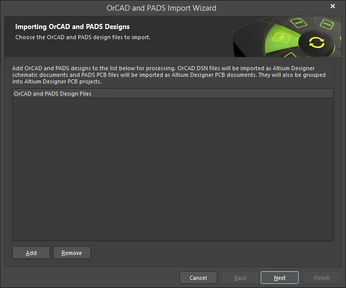
Use this page of the Wizard to add the OrCAD and PADS design files you want to import. Click Add to search for and select the desired files. Click Remove to delete a selected file.
Selecting the OrCAD and PADS Library Files
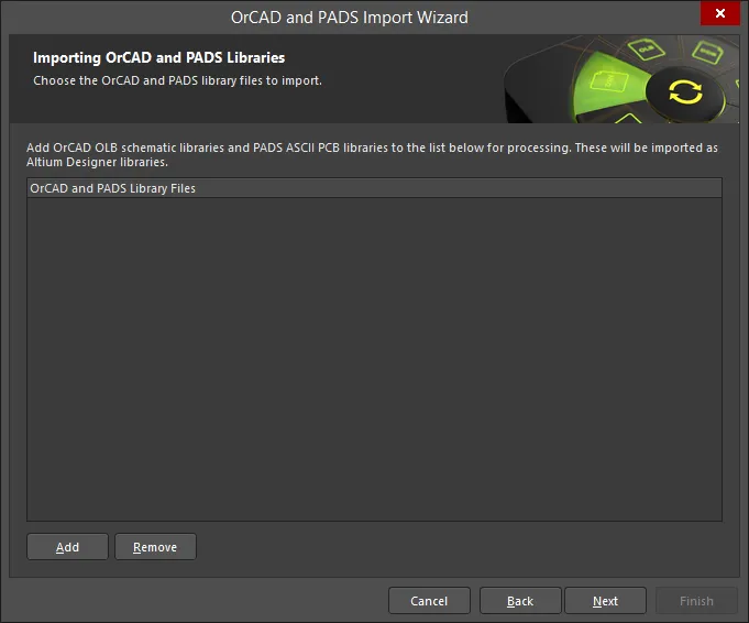
Use this page of the Wizard to add the OrCAD and PADS library files you want to import. Click Add to search for and select the desired files. Click Remove to delete a selected file.
Setting the Reporting Options
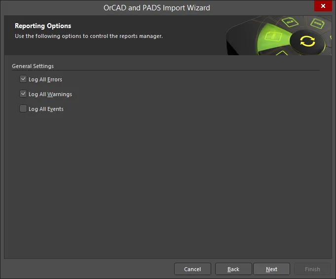
Use the Reporting Options page to set up general log reporting options.
Under General Settings, enable the desired options: Log All Errors, Log All Warnings, and Log All Events.
Setting the Schematic Options
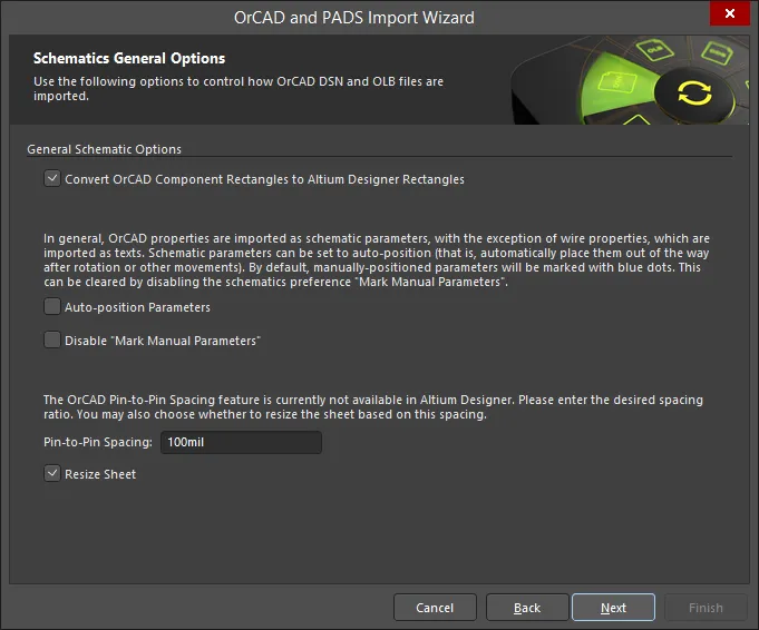
Use this page of the Wizard to control how OrCAD DSN (design) and OLB (library) files are imported.
Enable Convert OrCAD Component Rectangles to Altium Designer Rectangles if desired.
Usually, OrCAD properties are imported as schematic parameters (with the exception of wire properties) and are imported as texts. Schematic parameters can be set to auto-position by enabling Auto-position Parameters, which will automatically place them out of the way after rotation or other movements. By default, manually-positioned parameters will be marked with blue dots. To disable this default, enable Disable "Mark Manual Parameters".
The OrCAD pin-to-pin spacing feature currently is not available in Altium Designer. Enter the desired spacing ratio in the Pin-to-Pin Spacing textbox. If you want to also resize the sheet based on the entered spacing, enable Resize Sheet.
Setting Schematic Sheet Options

Use this page of the Wizard to control how OrCAD pages and junctions are imported.
OrCAD title blocks are imported as schematic components. Altium Designer also supports this feature; however, the title blocks in Altium Designer are limited to two types: Standard and ANSI and their graphics are not editable. If this is not desirable for your situation, templates can be used to provide a more flexible solution. Templates allow any graphical data to be placed onto a schematic sheet. Enable Strip OrCAD Title Blocks to strip the OrCAD title blocks. Check Enable Schematic Title Blocks if desired, then use the drop-down to select Standard or ANSI.
Enable the Force convert all I/O and Bi-directional pins to passive pins to automatically convert to I/O and bi-directional pins to passive pins.
Setting PCB and PCB Library Default Options
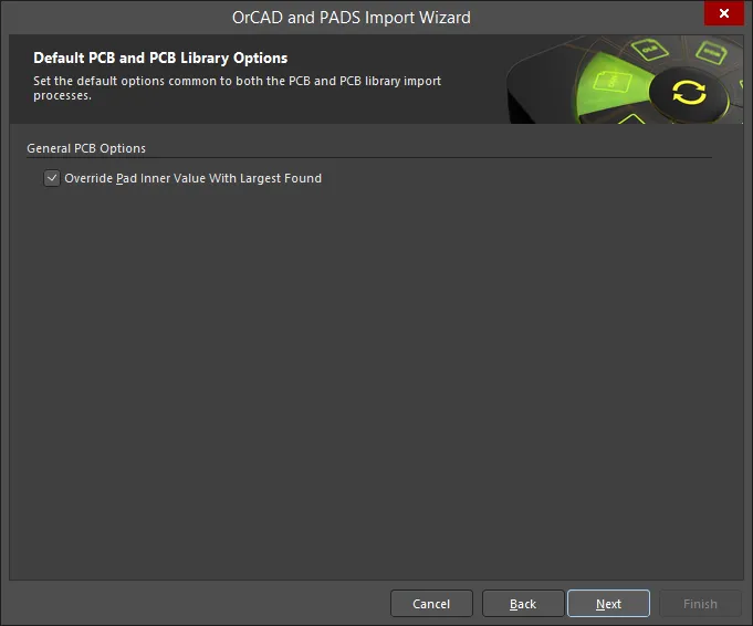
Use this page of the Wizard to set default options that are common to both the PCB and PCB Library import process.
Enable Override Pad Inner Value With Largest Found to specify that imported pads will have their sizes on the mid-layers set to the largest size found.
Setting Options for PCB Import Process
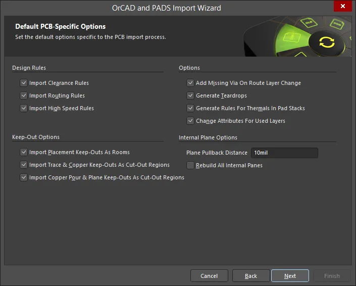
Use this page of the Wizard to set default options that are specific to the PCB import process.
Enable any Design Rules you want to import: Import Clearance Rules, Import Routing Rules, and Import Routing Rules.
Enable any Keep-Out Options you want to import: Import Placement Keep-Outs As Rooms, Import Trace & Copper Keep-Outs As Cut-Out Regions, and Import Copper Pour & Plane Keep-Outs As Cut-Out Regions.
Enable any desired miscellaneous Options:
- Add Missing Via On Route Layer Change
- Generate Teardrops
- Generate Rules For Thermals In Pad Stacks
- Change Attributes For Used Layers
Specify the desired Plane Pullback Distance in the textbox. Enable the checkbox to Rebuild All Internal Planes.
PCB and PCB Library Options

This page of the Wizard is used to review and edit options for each PADS PCB and PCB Library. Any unmapped layers are highlighted in pink.
Click Edit Mapping to open the PADS PCB Library ASCII File Import Options dialog.

All used PADS PCB layers must be mapped to an Altium Designer layer prior to import. The PADS PCB Library ASCII File Import Options dialog allows the user to map PADS PCB layers to an Altium Designer layer. The dialog also gives access to the Importer Settings dialog in which the user can control design rules, missing vias and keep-out conversions during the import process.
Setting Output Library Options
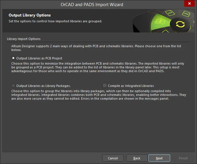
Use this page of the Wizard to control how the imported libraries are grouped.
Library Import Options – select one of the following options for how to group output libraries.
- Output Libraries as PCB Project – select to minimize the integration between PCB and schematic libraries. The imported libraries will only be grouped as a PCB project. They can be added to the list of libraries in the library panel later. This setup is most advantageous for those who wish to operate in the same environment as they did in OrCAD.
- Output Libraries as Library Packages – select to group the libraries into library packages. You can then select to compile the library packages as integrated libraries by enabling Compile as Integrated Libraries. Integrated libraries combine both PCB, schematic and PSpice libraries, enabling better interactions. Errors in the compilation are shown in the Messages panel.
Specifying the Output Directory

Use this page of the Wizard to review the output project structure and specify the output directory in which to import the files. Use the Browse Folder icon to search for and choose the Project Output Directory.
Click Menu to access options to edit the project structure:
-
Create Project – click to open the Create Project dialog to add a project.
Use the Create Project dialog to add a new project. -
Rename Project – click to rename the selected project. This option is available only when a
*.PrjPcb fileis selected. - Remove Selected Projects – click to remove the selected project from the PCB Projects structure.
- Reset Structure to Default – click to reset the PCB Projects structure to the defaults.
-
Add Designs to Project – click to add a design(s) to the project. This option is available only when a
*.PrjPcb fileis selected. - Remove Selected Designs - click to remove the selected design files.
Specifying the Output Library Directory

Use this page of the Wizard to review the output library structure and specify the output directory in which to import the library files. Use the Browse Folder icon to search for and choose the Library Output Directory.
Executing Import Process

This page shows a green progress bar of the import process.
Closing the Wizard
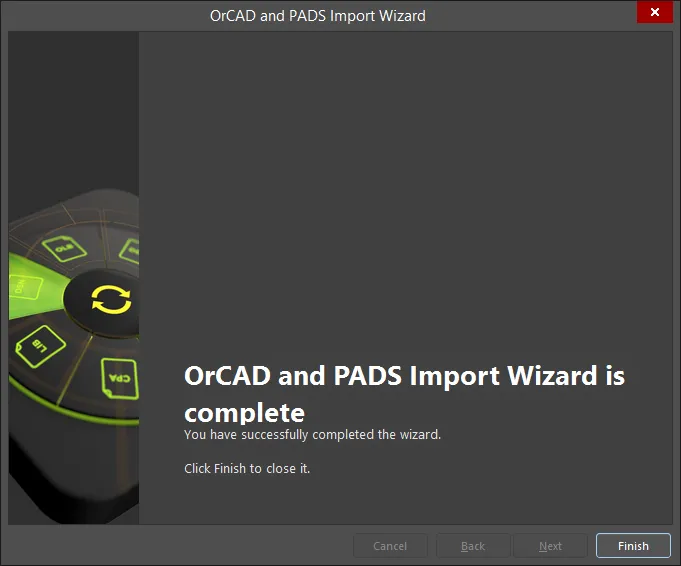
The OrCAD and PADS Import Wizard has completed. The Messages panel appears with any relevant messages. Click Finish to close the Wizard. If any warnings were generated during the import process, a *.LOG file opens showing the warnings.
PADS and OrCAD files translate as follows:
-
PADS ASCII PCB Layout (
*.ASC) files translate to Altium Designer PCB files (*.PcbDoc). -
PADS ASCII PCB Library files translate into Altium Designer PCB library files (
*.PcbLib). -
OrCAD Capture (
*.DSN) files translate to Altium Designer schematic files. Each page within a .DSN file will be imported as a single Altium Designer schematic file (*.SchDoc). Design caches within a .DSN file will be imported as a schematic library (*.SchLib). Design hierarchy is maintained, including complex hierarchy. -
OrCAD schematic library (
*.OLB) files will be translated into Altium Designer schematic library files (*.SchLib). -
The files will be grouped into an Altium Designer PCB project (
*.PrjPCB) that is automatically created. - Translated OrCAD libraries are automatically grouped into one PCB project.
Working with Imported Documents
In OrCAD Capture, all design work begins on the page, which is the logical working area of the design, and there can be multiple schematic pages within a single OrCAD schematic design file (*.DSN file). In Altium Designer, the logical design area begins with a document, and for each document, there is a file stored on the hard drive.
This means that each Altium Designer schematic sheet (page) is represented by is schematic document file, which is a key conceptual difference to keep in mind. Note that Altium Designer can also include multiple documents of varying types (beyond just schematic and PCB design documents), depending on the nature of the design project.
Panels
Many elements of the Altium Designer environment will appear familiar to OrCAD users, such as the Projects panel, which is similar to the OrCAD Project Manager. Since the Projects panel is not limited to schematic design data, it can include the PCB, all libraries, output files, as well as other project documents, such as non-native files (PDFs, text files, spreadsheets, etc.).
Project Structure
OrCAD Capture, like Altium Designer, supports flat and hierarchical designs.
Capture presents a schematic, shown as a folder icon in Capture's Project Manager, and this contains pages shown as schematic sheet icons. Each Capture schematic can be made up of one or more pages, and a typical flat Capture design is one schematic (folder), with the design being drawn on as many pages as required in that schematic.
The schematic folder at the top of a hierarchy, which directly or indirectly refers to all other modules in the design, is called the root module. In the OrCAD Project Manager, the root module has a backslash on its folder icon.
Altium Designer presents a hierarchy of related schematics, where the sheet-to-sheet structure is typically defined by Sheet Symbols. The equivalent Capture construct is a Hierarchical Block symbol, which references the lower-level schematic.
Net Connectivity
In OrCAD Capture, net connectivity is made using net aliases, off-page connectors, hierarchical blocks and ports, and globals. Nets between schematic pages within a single schematic folder are connected through the off-page connectors while the hierarchical blocks and ports connect the nets between the schematic folders. Globals are used to connect power/ground nets throughout the design.
Altium Designer uses a similar set of net identifiers to create net connectivity. Within a schematic sheet you can use Wires and Net Labels. Between schematic sheets, nets in a flat design are typically connected using Ports, but Off-Sheet Connectors are also available. Nets in a hierarchical design are connected from a Port on the lower sheet to a Sheet Entry of the same name in the sheet symbol that represents the lower sheet. Power/ground nets are connected using Power Ports.
If desired, you can enable the Convert Orcad Off-Page connectors as Altium Ports (instead of defaults Off-sheet connectors) option on the Schematics General Options page to eliminate the manual process needed to convert off-page connectors to ports.
