
Polygons on Signal Layers

Altium Essentials: PCB Polygon Pour and Planes
This content is part of the official Altium Professional Training Program. For full courses, materials and certification, visit Altium Training.
 being used to create a large GND area on a board")
A polygon pour (brighter red) being used to create a large GND area on a board

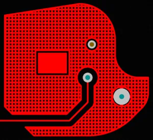
A polygon pour is shown as solid and hatched, demonstrating varying clearances and controlled connection style and air gap.
A polygon pour is a group design object that is made up of simpler primitive objects, either regions, or tracks and arcs. Polygon pours are used to create a solid or hatched (lattice) area on a PCB layer, using either region objects or a combination of track and arc objects. Also referred to as copper pours, polygon pours are similar to a region except that they can fill irregularly shaped areas of a board as they automatically pour around existing objects, connecting only to objects on the same net as the polygon pour.
On a signal layer, you can place a solid polygon pour to define an area for carrying large power supply currents, or as a ground-connected area for providing electromagnetic shielding. Hatched polygon pours are commonly used for ground purposes in analog designs.
A polygon pour that is placed on a signal layer creates a polygonal (multi-sided) area of copper that can either be solid or hatched. As they are poured, polygons automatically allow for clearances around electrical objects belonging to a different net, connect to objects of the same net, and fill irregularly shaped areas. Clearances and connection properties are controlled by the applicable Electrical Clearance and Polygon Connection Style design rules.
Placing a Polygon Pour
Polygon pours can only be placed in the PCB editor. To place a polygon pour directly, first switch to the required layer. After launching the polygon pour placement command (Place » Polygon Pour), the cursor will change to a crosshair, and you will enter polygon pour placement mode. Position the cursor, then click or press Enter to place. Continue placing further polygon pours or right-click or press Esc to exit placement mode.
Corner Modes
While placing a polygon pour, there are five available corner modes (45°, 45° arc, 90°, 90° arc, and Any Angle), four of which also have corner direction sub-modes. During placement:
- Press Shift+Spacebar to cycle through the available corner modes.
- Press Spacebar to toggle between the two corner direction sub-modes (except for the Any Angle mode).
- When in either of the arc corner modes, hold the , or . key to shrink or grow the arc. Hold the Shift key as you press to accelerate arc resizing.
- Press Backspace to remove the last corner.
- Press the 1 shortcut key to toggle between placing two edges per click or one edge per click. In the second mode, the dashed edge is referred to as the look-ahead segment (as shown in the last image in the set below; refer to the Understanding the Look-Ahead Feature section for more information).


Press Shift+Spacebar to cycle through the five available corner modes; press the 1 shortcut to toggle placement between two edges or one edge.
Understanding the Look-Ahead Feature
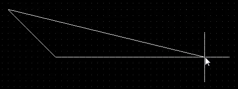
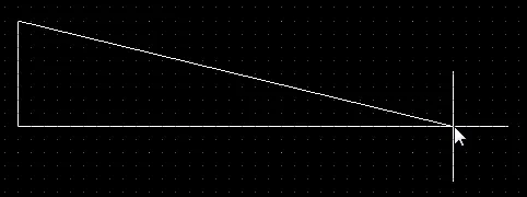
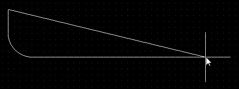
There are many situations during PCB design where you need to be able to predict where a future track segment or object edge must go without committing to place that object. To support this requirement, Altium Designer includes a feature called Look-Ahead. When Look-Ahead is enabled, the track/object edge currently attached to the cursor is not placed when you click; only the previous segment is placed. In other words, the last segment allows you to look ahead to where the future segment will be placed.
Press the 1 shortcut key during object placement to toggle Look-Ahead on or off. Note how the display changes to display each mode. In track placement, the segments to be placed with the next click are shown as hatched, and the Look-Ahead segment is shown as hollow or empty. In solid object placement, the edges to be placed with the next click are shown as solid white lines and the Look-Ahead edge is shown as a dashed white line.
The following images show how the display of track segment changes when the Look-Ahead feature is on and off.
 and off (second image). The next mouse click will place the hatched track segments.") Track placement with Look-Ahead on (first image) and off (second image). The next mouse click will place the hatched track segments.
Track placement with Look-Ahead on (first image) and off (second image). The next mouse click will place the hatched track segments.
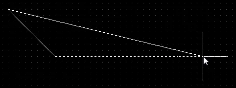
The Look-Ahead feature also works during polygon pour placement. Press the 1 shortcut key during placement to toggle it on and off (note that this shortcut only works during object placement). The following images show the first corner placement of a polygon pour.
 Look-Ahead is on. With the next mouse click, the solid line becomes a polygon edge but not the dotted line. Note the solid return line. It shows how the polygon will be closed if you terminate polygon placement.
 Look-Ahead is off. With the next click, both of the solid lines become polygon edges. Note the solid return line. It shows how the polygon will be closed if you terminate polygon placement.
Editing a Polygon
Moving a Polygon Pour
Click on the actual shape of a selected polygon pour (away from its editing handles) and drag to move it. Hold down the Shift key to select multiple polygon pours to move.
Additional actions that can be performed during movement are:
- Press the Spacebar to rotate the polygon pour counterclockwise or Shift+Spacebar for clockwise rotation. Rotation is in accordance with the value for the Rotation Step defined on the PCB Editor – General page of the Preferences dialog.
- Press the L key to flip the polygon to the other side of the board.
- Press the X or Y keys to mirror the polygon along the X-axis or Y-axis respectively.
Alternatively, you can right-click over a polygon pour and choose the Polygon Actions » Move Polygon command from the context menu. After launching the command, the polygon pour will attach to the cursor, drawn in outline mode. Move the polygon pour to the required position, then click or press Enter to effect placement.
Reshaping a Polygon Pour
 A polygon pour with 90º arc corners being resized.
A selected polygon pour contains two types of points or "handles" with which to edit the shape of the polygon pour.
- Full Handles - these filled handles are located at the corners of the polygon.
- Empty Handles - these blank handles are located in the centers of the segments created by the Full Handles.
An existing polygon can be reshaped by moving these handles, or vertices, located at each corner or at the center of each edge.
To modify the polygon shape:
-
Click and select a polygon, which will highlight the vertices for the polygon and change the cursor to a crosshair.
- Click, hold and drag a Full Handle to move that corner.
- Click, hold and drag along an edge to move the entire edge.
- Click, hold and drag an Empty Handle to move the whole side (for track and for arc).
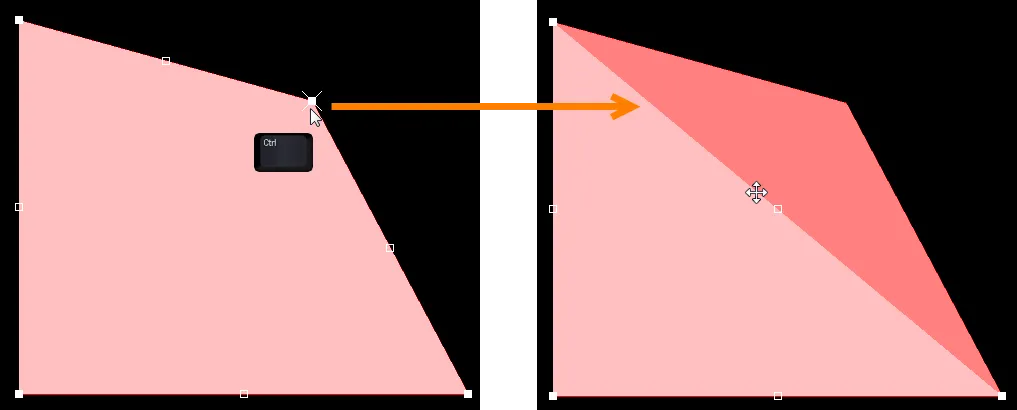
- Ctrl+Click on an Empty Handle to break that edge into two edges. Ctrl only needs to be held at the beginning of movement. The Shift+Spacebar hotkeys can then be used to cycle through modes (arc, miter, and any angle).

The top images show empty handle editing. In the bottom images, Ctrl has been clicked while grabbing the handle to move for editing. -
If the 'any angle' placement mode creates unwanted vertices, click and hold on the vertex and drag the edge to reduce the vertices on that edge to one. To delete a vertex, click and hold on the vertex as if you were going to move it then press the Delete key.
- When you have finished, right-click and then select Polygon Actions » Repour Selected to repour the polygon in its new shape.
Modifying Polygon Pour Border
In addition to vertex editing, you can also use the Polygon Actions » Modify Polygon Border right-click command to easily change the shape of polygons. Once the command is launched, the cursor becomes a crosshair. Each time you click, a new vertex is added. As during polygon placement, the Shift+Spacebar shortcuts can be used to change corner shapes.
Resizing a Polygon Pour
To switch from editing the shape to editing the size of the selected polygon pour object currently under the cursor, you can right-click over a selected polygon pour object and then choose the Polygon Actions » Resize Polygon command from the context menu. After launching the command, the polygon editing mode will change from that of reshaping, to that of resizing. Confirmation of this is visually conferred by the editing handles along each edge of the polygonal shape, being replaced with eight editing handles located at the corners (and centers) of the object's bounding rectangle.
- Click and drag a corner editing handle to resize the polygonal pour in the vertical and horizontal directions simultaneously.
-
Click and drag a center editing handle to resize the polygonal pour in the vertical or horizontal direction separately.
After modifying the size or location of the polygon pour, it will become marked as modified. If the Repour Polygons After Modification option is enabled on the PCB Editor - General page of the Preferences dialog, the polygon (and all of its dependants) will be repoured automatically. If this option is not enabled, the polygon pour will not be repoured.
To switch from editing the size back to editing the shape, right-click over a selected polygon pour object, whose size is currently being modified, and choose the Polygon Actions » Edit Polygon Shape command from the context menu.
Polygon Pour Properties

The Polygon Pour mode of the Properties panel
| Actions |
|
| Net Information | Information about the net that the polygon pour belongs to, as well the differential pair, if that net is a member. Class information is also shown where appropriate. Refer to the PCB Placement & Editing Techniques page to learn more about net information. |
| Net | Net that this polygon pour is a member of. All nets for the active board design will be listed in the drop-down list. Select No Net to specify that the polygon is not connected to any net. The Net property of a primitive is used by the Design Rule Checker to determine if a PCB object is legally placed. Alternatively, you can click on the Assign Net icon ( |
| Layer | Use the drop-down to select the layer on which the polygon pour is placed. |
| Name | Specify a suitable name for the polygon. As well as helping identify each polygon, the name can be used to target a specific polygon (or family of polygons) in a design rule. By default, automatic polygon naming based on the layer and the net is applied to the polygon. Naming is based on the chosen naming scheme specified in the Polygon Naming Scheme field of the Board mode of the Properties panel. If you have entered a custom name and wish to revert to automatic naming, simply clear the field and press Enter. |
| Area | The area that the given polygon pour encapsulates listed in square millimeters or square inches. |
| (X/Y) | Current location of the first vertex of this polygon pour in the design space, relative to the user-definable origin. Click the |
| Fill Mode | Choose the fill mode for the polygon pour. There are three modes available, each with its own advantages and options. Learn more about Polygon Pour Fill Modes. |
| Pour Over Same Net | Use the drop-down to control the pouring behavior when objects on the same net are encountered. Learn more about Connecting the Polygon Pour to a Net. |
| Remove Dead Copper | When a polygon is poured, there can be regions (islands) of the polygon that are completely isolated from the connected net due to the presence of other tracks, pads, etc. If this option is enabled, any area of the polygon that does not include at least one connection to another net object is automatically removed. Note that if your polygon does not enclose any pads on the assigned net, then it is all dead copper and will all be removed. In this situation, the outline of the polygon is still shown to indicate that a polygon exists in this location. |
| Optimal Void Rotation | Enable this option to ensure that the polygon's edges are arranged to give the maximum neck width where a polygon passes between adjacent objects that belong to other nets. Polygon arcs are replaced by short straight edges, whose lengths are determined by the Arc Approx. setting. |
| Outline Vertices | Use this region to modify the individual vertices of the currently selected polygon pour object. You can modify the locations of existing vertices, add new vertices or remove them as required. Arc connections between vertex points can be defined and support is provided for exporting vertex information to and importing from a CSV-formatted file.
To export the entire grid contents to file in CSV format, right-click anywhere within the grid and choose the Export To CSV command. The Export Outline Vertices dialog will appear in which to determine where, and under what name, the file is saved. By default, the file will be named |
Polygon Pour Fill Modes
 then poured using tracks/arcs (Hatched).")
The same polygon poured using regions (Solid) then poured using tracks/arcs (Hatched).
The polygon pour placement engine can construct polygons from either solid regions or from a combination of tracks and arcs, depending on the fill mode selected in the Properties panel. The preview image changes to present a graphical depiction of a solid polygon pour, and associated options are provided in the panel. There are three supported fill modes.
Solid
When this mode is selected, the polygon is internally constructed from solid region objects, with a separate region for each contiguous area of copper in the completed polygon.
The following associated options are provided in the Properties panel when this mode is selected ( ).
).
| Remove Islands Less Than | Specify an area value. Any areas of copper whose area is smaller than this value will be removed. |
| Arc Approx. | Specify the maximum deviation from a perfect arc (curved edges are created from multiple short, straight edges). Reducing this value will result in a larger number of straight edges being used to give a better approximation of an arc. |
| Remove Necks Less Than | Specify a width value. Narrow slivers of copper with a width smaller than this value will be removed. Note that when this option has a larger value, there will be a greater number of tight locations where the polygon cannot pour. Typically, this is set to be no smaller than the smallest width track used in the design or the smallest copper width supported by the fabricator. Enable the Obey Rules option to take the value from the applicable minimum Width constraint. |
Hatched
When this mode is selected, the polygon is created from track and arc objects. The outline of a hatched polygon is created from tracks and arcs with the user-defined edge of the polygon at the center-line of the outline tracks and arcs.
The following associated options are provided in the Properties panel when this mode is selected ( ).
).
| Track Width | Specify the width of track used to create the polygon. |
| Grid Size | Specify the spacing, or grid, that the tracks are placed on for the hatched polygon. |
| Surround Pad With | Specify the shape used to surround the pads: Arcs or Octagons. |
| Hatch mode | There are four modes available: 90 Degree, 45 Degree, Horizontal, or Vertical. |
| Min Prim Length | Specify how short the track/arc objects in the fill mode are allowed to be. |
| Obey Polygon Cutout | Enable this option if the hatched polygon pour should not encroach boundaries of a polygon pour cutout. When this option is disabled, the centerlines of the polygon pour tracks will be placed along the boundaries of a polygon pour cutout. |
None
This mode is essentially the same as the Hatched mode. It also uses tracks and arcs to define the boundaries, but the fill-in tracks and arcs are not added.
The following associated options are provided in the Properties panel when this mode is selected ( ).
).
| Track Width | Specify the track width for the polygon pour outline. |
| Surround Pad With | Specify the shapes to surround the pads: Arcs or Octagons. |
| Min Prim Length | Specify how short the track/arc objects in the fill mode are allowed to be. |
| Obey Polygon Cutout | Enable this option if the outline polygon pour should not encroach boundaries of a polygon pour cutout. When this option is disabled, the centerlines of the polygon pour tracks will be placed along the boundaries of a polygon pour cutout. |
Connecting the Polygon Pour to a Net
A polygon can be attached to a net. Select the required net in the Net drop-down in the Properties panel. The polygon pour will connect to each pad and via of this net that is found within the outline of the polygon, in accordance with the applicable Polygon Connect Style design rule. Note that the rule supports defining different methods of connection for thru-hole pads, SMD pads, and vias, if required. The clearance between the polygon and objects belonging to other nets is determined by the applicable Electrical Clearance design rule.
How the polygon pour treats other objects on the same net, including routing tracks, arcs, fills, and regions, is determined by the option selected in the Pour Over Same Net drop-down in the Properties panel when the polygon pour is selected:
- Don't Pour Over Same Net Objects – choose this option if you specifically do not want the polygon to pour over track, arc, fill, region, or polygon objects in this (or any other) net, i.e. select to pour the polygon in free space only.
- Pour Over All Same Net Objects – choose this option if you want the polygon to be poured in free space and also over all objects (i.e. tracks, arcs, fills, regions, other polygons) on the same net as the polygon that are within the polygon's area. For example, existing routes on that net will be completely covered by the polygon.
- Pour Over Same Net Polygons Only – choose this option (default) if you want the polygon to only pour it in free space and over existing polygon pour objects inside its boundary that belong to the same net. The polygon will pour around all other objects (tracks, arcs, fills, and regions) regardless of the net to which they belong.
Shelving and Restoring a Polygon Pour
During the design process, it is normal for changes to occur – components might be added or changed, routing may need to be updated, etc. To simplify the management of existing polygons during this process, they can be shelved. This temporarily hides them from display and the DRC and net connectivity analysis engines but retains them in the PCB database (i.e. they are not destroyed and can be restored at any time). This allows changes to the board layout to be made both with visual ease, and without the impact on performance – both editing and DRC – that visual polygon pours can bring.
- To shelve all polygon pours in the current design, select Tools » Polygon Pours » Shelve <n> Polygon(s) from the main menus (where <n> is the number of polygon pours that have been detected in the design).
- To restore all shelved polygon pours, select Tools » Polygon Pours » Restore <n> Shelved Polygon(s) command from the main menus (where <n> is the number of polygon pours that are currently shelved). All restored polygons are treated as though they have been modified. If the Repour Polygons After Modification option is enabled on the PCB Editor - General page of the Preferences dialog, the polygon pours, and all their dependents, will be automatically repoured. If this option is disabled, the restored polygon pours will not be repoured.
- You also can selectively shelve polygons from the right-click Polygon Actions sub-menu commands or the Polygon Pour Manager dialog.
Repouring a Polygon
If you have changed the design within a polygon, once it has been restored, it will need to be repoured to clear any violations created by the design changes. There are a number of ways a polygon can be repoured (rebuilt) in the current document.
To repour a polygon, right-click on the polygon then select a Repour command from the Polygon Actions sub-menu or use the appropriate Repour command in the Tools » Polygon Pours sub-menu:
- Repour Selected - repour all selected polygon pours (and their dependents).
- Repour All - repour all defined (and non-shelved) polygon pours.
- Repour Violating Polygons - repour all violating polygon pours.
- Repour Modified - repour all modified polygon pours. A modified polygon pour is one that has been changed in some way, but has not yet been repoured. Its IsModified property - which can be seen from the PCB List panel for a selected polygon pour - is enabled (True).
Polygon pours can also be repoured in the Polygon Pour Manager dialog (Tools » Polygon Pours » Polygon Manager) by selecting the required polygon then clicking the Repour button.
Confirm the changes in the Confirm dialog.
Configuring the Pour Order
When two polygons overlap, Altium Designer needs to know which one should occupy the shared area where they overlap. This is done by defining the pour order, with the higher-order polygon having precedence and pouring over the shared area. The pour order of overlapping polygons can be configured interactively by right-clicking over a selected polygon pour and choosing one of the following commands from the context menu:
-
Polygon Actions » Bring to front - change the pour order, so that the selected polygon is in front of all other overlapping polygons (and therefore has the highest precedence).
-
Polygon Actions » Send to back - change the pour order so that the selected polygon is behind all other overlapping polygons (and therefore has the lowest precedence).
The changed order will be seen visually in the design space once the polygon pour, which is now classed as modified, is repoured.
Controlling the Polygon Connection Style
Main page: Polygon Connect Style Design Rule
How the polygon connects to pads on the net to which it is attached is controlled by the applicable Plane » Polygon Connect Style design rule (Design » Rules).

How the polygon connects to pads on the net is determined by the Polygon Connect Style design rule.
Three connection options are available:
- Relief Connect - a spoke-style connection is created. Define the Number of conductors, the Angle of these conductors (90º or 45º), Conductor Width, and the Air Gap Width (the clearance between the edge of the pad and the edge of the polygon surrounding the pad).
- Direct Connect - the polygon effectively pours over the pad creating solid copper to the pin.
- No Connect - the pads on the net will be isolated from the polygon.
Controlling the Polygon Clearance
Main page: Clearance Design Rule
Like any object placed on a signal (copper) layer, the clearance of a polygon from objects that it is poured around is controlled by the applicable Electrical Clearance design rule.
 The clearance from the polygon to objects on other nets is controlled by the Electrical Clearance design rule.
It is common practice to have a larger clearance between a polygon and other net objects. To achieve this, a polygon-specific Electrical Clearance design rule can be defined. An example of this is shown in the image above. Remember that the Polygon Clearance rule must also have a higher Priority than any general clearance rule to have any effect.
Polygon Pour Cutouts
A polygon pour cutout is essentially a negative copper region in which you are defining a void or hole in the polygon. To define a cutout in a polygon:
- Select the Place » Polygon Pour Cutout command from the main menus.
- The cursor will change to a crosshair, starting inside the boundary of the polygon. Click to define the starting location.
- Move the cursor across the polygon. Press Shift+Spacebar to cycle through the region corner modes.
- Continue to click and move the mouse to define the cutout outline.
- Right-click to exit polygon cutout placement mode.
- The original polygon must now be repoured. Click on it to select it, then use the Tools » Polygon Pours » Repour Selected command from the main menus - it will pour around the new cutout.
The cutout is actually a Region object with the Polygon Cutout option enabled. It can be moved, resized, or deleted if required. To resize a cutout, click on it once to select it, then click and hold to drag an edge or a vertex. Remember that the polygon must be repoured whenever the cutout is changed.
; the polygon has been repoured (second image).")
The cutout has been placed (first image); the polygon has been repoured (second image).
Creating a Polygon Pour From a Set of Tracks
As well as defining areas of electrical copper on a board, polygons and solid regions are also used to define other polygonal-shaped design objects, such as a special symbol or a company logo. If an outline of the required shape has been defined in another design tool, such as AutoCAD, it can be exported as a DXF file then imported into Altium Designer. That outline can then be converted into a polygon or a solid region.
To convert a closed boundary made up of selected track and/or arc objects to a polygon, select all primitives that form the closed shape and then select Tools » Convert » Create Polygon from Selected Primitives from the main menus.
Note that:
- The polygon will be created on the current (or active) layer, not the layer that the selected tracks are on. This means you can define the shape on a Mechanical Layer then create the polygon on a signal layer.
- The originally selected primitives are not removed – they will still exist after the polygon has been created and will remain selected. The new polygon is poured inside the selected objects.
- The edge of the new polygon will lay along the centerline of the selected objects that were used to create it.
- If the polygon is created on the same layer as the selected tracks, it will pour within the tracks in accordance with the applicable Electrical Clearance Design Rule.
- The polygon will be created with its fill mode set to None. Double-click to repour the new polygon as solid or hatched.
Slicing a Polygon Pour
A single polygon pour can be sliced into two or more separate polygon pours. To do this:
- Ensure that the correct layer is made the current layer since the slicer will only work provided the current layer is the layer on which the polygon pour to be sliced resides.
- Select the Place » Slice Polygon Pour from the main menus (or the Slice Polygon Pour command on the Active Bar, or the Polygon Actions » Slice Polygon Pour command from the polygon pour's right-click menu).
- When you select the command, you are in slice mode (similar to track placement mode), and the cursor will change to a crosshair. Starting outside the boundary of the polygon, click to anchor the starting point for the slicing line (the first track segment).
-
Move the cursor across the polygon. The slicing process uses the Line placement mode to define both the slice path and width. When defining the slice:
-
Press Shift+Spacebar to cycle through the line placement corner modes.
-
Press Spacebar to toggle between the Start and End corner modes.
-
Press Backspace to remove the last-placed corner.
-
Press Tab to access the Line Constraints dialog to change the width of the line and/or the current layer for placement.

The Line Constraints dialog.- Line Width - use this field to enter a new width for the line. This new width will be applied to the segment currently being placed.
- Current Layer - use this field to switch the layer on which the line is placed. The drop-down menu lists all currently defined (and enabled) layers for the board. The chosen layer will apply to the look-ahead segment of line, that is, the segment after the one currently being placed.
-
- Click to anchor a series of vertex points that define the slice line.
- Once the slicing line has been placed across and out the other side of the polygon, right-click or press Esc to terminate line placement.
- Right-click a second time to terminate slicing. A Confirm dialog will appear asking if you want to split the polygon; click Yes to split it.
Since these are now two independent polygons, each can be edited and repoured as required.
Combining Selected Polygon Pours
Two or more polygon pour objects can be combined by performing the following sequence of actions:
- Place new (or drag existing polygon pours) so that they are overlapping each other as required.
- Select all polygon pours that are to be combined.
- Right-click over one of the pours in the selection then choose the Polygon Actions » Combine Selected Polygons command from the context menu.
Subtracting Selected Polygon Pours
One or more polygon pour objects can be subtracted from another 'base' polygon pour by performing the following sequence of actions:
- Place new or drag existing polygon pours so that they are overlapping the required base polygon pour - this is the pour from which to be 'subtracted'.
- Select the base polygon pour, right-click, and then choose the Polygon Actions » Subtract Polygons From Selected command from the context menu.
- Select the polygons to be subtracted.
- Right-click or press Esc to complete the process.
Exploding a Polygon Pour to Primitives
A polygon pour can be reverted to the various primitives from which it was made by choosing the Tools » Convert » Explode Polygon to Free Primitives command from the main menus or by right-clicking over a placed polygon pour (selected or not) then choosing the Polygon Actions » Explode Polygon To Free Primitives (or Explode Selected Polygons To Free Primitives) command from the context menu. Solid polygons will revert to region primitives, while hatched polygons will revert to tracks and arcs. Once exploded, a polygon pour object can no longer be manipulated as a group object.
Although there is no actual command to regroup an exploded polygon, you can use the Undo command to achieve this.
The Polygon Pour Manager Dialog
The Polygon Pour Manager dialog provides a high-level view of all polygons that currently exist in the PCB design space. The dialog also allows you to name/rename each polygon, set the pour order of polygons, perform repouring or shelving actions on selected polygons, and add/scope design rules for selected polygons.
To open the Polygon Pour Manager dialog, select the Tools » Polygon Pours » Polygon Manager command from the main menus or right-clicking over a placed polygon pour in the design space then choose the Polygon Actions » Polygon Manager command from the context menu.

The Polygon Pour Manager dialog gives you full control over all the polygons in the design.
After launching the command, the Polygon Pour Manager dialog will open. The dialog can be used to perform all non-graphical editing of polygon pours in the design including controls to:
- Rename polygons (including the ability to use the Auto-Naming feature).
- Set polygon pour order.
- Perform repouring of all or certain polygons (modified/selected/violating).
- Shelve or unshelve all or selected polygons.
- Lock or unlock all or selected polygons.
- Ignore or keep violations for all or selected polygons (with respect to the Online DRC).
- Add/scope the polygon connection style and clearance design rules.
- Add polygon classes for selected polygons.
- Create a new polygon from either a selected polygon or the board outline.
Options and Controls of the Polygon Pour Manager Dialog
View/Edit
This is a list of all existing polygons in the PCB document. The Pour Order list groups polygon outs by layer, which presents only those polygon pours on the same layer as the currently selected polygon pour (or first selected if multiple pours are selected across different layers). Click a column heading to sort by that column. Polygon names may be edited. Once named, they can be used to scope polygon rules or create queries. You may select one or more polygons in the grid (Ctrl+Click) then perform the grid functions described below.
Grid
-
Name – specify a suitable name for the polygon. As well as helping identify each polygon, the name can be used to target a specific polygon (or family of polygons) in a design rule. By default, automatic polygon naming is applied to the polygon. Naming is based on the chosen naming scheme specified in the Polygon Naming Scheme field of the Board mode of the Properties panel. If you have entered a custom name and wish to revert to automatic naming, simply clear the field and press Enter.
- Area – the area that the given polygon encapsulates, listed in square millimeters.
- Net – the assigned net.
- Shelved – enable to shelve the polygon.
- IsModified – shows if the polygon has been modified.
- Locked – toggle to lock/unlock the polygon.
- Ignore On-Line DRC Violations – enable to ignore violations.
Buttons
-
Repour – use the sub-menus to select which polygon(s) to repour:
Modified Polygons,Selected Polygons,Violating Polygons, orForce Repour All Polygons. The number listed in parentheses after the first three choices is the total number of polygons affected with that specific action. -
Shelving – use the sub-menus to select which polygon(s) to Shelve or Unshelve:
All PolygonsorSelected Polygons. To commit the action, click Apply or OK. -
Locking – use the sub-menus to select which polygon(s) to Lock or Unlock:
All PolygonsorSelected Polygons. To commit the action, click Apply or OK. -
Violations – use the sub-menus to selectively Ignore Violations or Keep Violations of online DRC violations for
All PolygonsorSelected Polygons. To commit the action, click Apply or OK. -
New Clearance Rule – click to open the Edit PCB Rule dialog to create a clearance rule with a new query for the selected polygons. This rule specifies the minimum clearance between any two primitives on a copper layer.
-
New Connect Style Rule – click to open the Edit PCB Rule dialog to create a polygon connection style rule with a new query for the selected polygons. This rule specifies the style of the connection from a component pin to a polygon plane.
-
New Polygon Class – click to create a polygon class for the selected polygons. You will be required to provide a name for the new polygon class in the Object Class Name dialog. An object class is a set of objects treated as a group used by the design rules for example.
-
New Polygon from – click to create a new polygon then choose:
-
Selected Polygon – click to create a new polygon in which the settings are cloned from the selected polygon by default. The new polygon pour is automatically added to the list of existing pours in the View/Edit and Pour Order region of the Polygon Pour Manager dialog.
-
Board Outline – click to create a new polygon from the board outline. The new polygon pour is automatically added to the list of existing pours in the View/Edit and Pour Order region of the Polygon Pour Manager dialog.
The new polygon is inserted into the repour order according to the following logic:
Source Polygon
Other Polygon
New Polygon
Same layer
Same layer
Below Both
Same layer
Different layer
Below Source
Different layer
Same layer
Above Source
Different layer
Different layer
Above Source
-
Pour Order
This region lists the order in which polygons will be poured. The preview image to the right shows a graphical representation of the polygon pours.
- Move Up – click to move the selected polygon up in the repour order list. The higher the polygon is in the list, the earlier it gets re-poured relative to other polygons lower in the list.
- Move Down – click to move the selected polygon down in the repour order list. The lower the polygon is in the list, the later it gets re-poured relative to other polygons higher in the list.
- Auto Generate – click to have the system determine the pour order of polygons from smallest to largest. You can then use the Move Up and Move Down buttons to fine-tune the pour order if required.
- Animate Pour Order – click to preview the order of polygon pours in the graphical representation of the PCB in the preview area.
Polygon Pour Properties
The far-right region presents the properties of the selected polygon pour. The properties can be edited directly in the Polygon Pour Manager dialog, or they can be edited in the Properties panel when the polygon pour is selected in the design space. Refer to the Polygon Pour Properties section to learn more about the properties available for polygon pours.
Notes about the Polygon Pour Manager dialog:
- A polygon is automatically named during placement; you can rename it to suit your design. Note that the Name can be used to scope design rules targeting a polygon.
- The Pour Order region allows you to rearrange the pour order of polygons with the Move Up, Move Down, and Auto Generate buttons. You can also change the order using mouse drag-and-drop functionality, which is far more expedient in designs featuring many polygon pours.
- Pour order can be important when there is a polygon that is completely enclosed within another polygon. Typically, you would order from the smallest polygon down to the largest polygon.
- The Auto Generate button will order the polygons from the smallest area to the largest area on a layer-by-layer basis.
- If you click the Repour button, you have the choice of repouring modified polygons, selected polygons, polygons that have violations, or all polygons, or Force Repour All Polygons. Update progress can be monitored in the status bar.
Once all editing/management of polygons has been performed, click OK. Changes will be effected at this point. If the Repour Polygons After Modification option is enabled on the PCB Editor - General page of the Preferences dialog, the polygon(s) will be repoured automatically. This also will include dependent polygon(s) if the Repour all dependent polygons after editing option is also enabled. If these options are not enabled, the polygon pour(s) will not be repoured. In this latter case, use the applicable Repour command from the Tools » Polygon Pours sub-menu.
Browsing Polygons
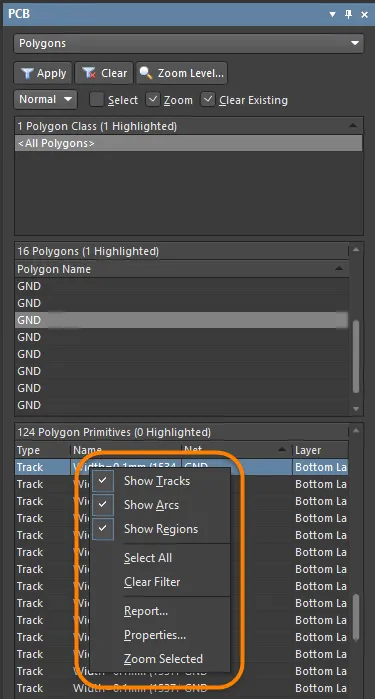
In the PCB panel’s Polygons mode, its three main regions change to reflect the polygon hierarchy of the current PCB design (in order from the top):
- Polygon Classes.
- Individual Polygons within a class.
- Individual Polygon Primitives that constitute a Polygon.
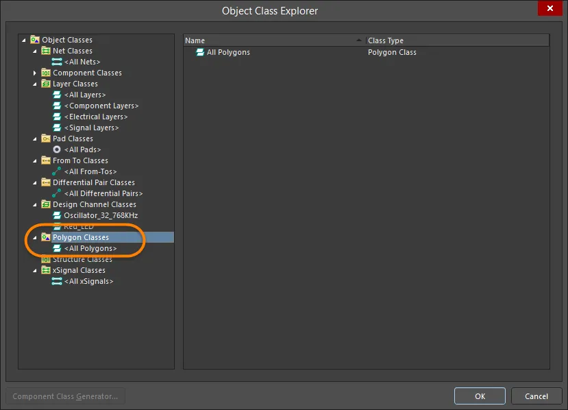
For full control and editing of Polygon Classes, open the Object Class Explorer dialog using the Design » Classes command from the main menus. From this dialog, you can view/modify the polygon membership of the class, rename it, or add additional classes.
In the PCB panel, right-clicking on a polygon entry then selecting Properties (or double-clicking on the entry) will open the Polygon Pour mode of the Properties panel in which you can view/modify the properties as required. Similarly, right-clicking on a polygon primitive entry then selecting Properties (or double-clicking on the entry directly) will provide access to the relevant Properties panel mode in which you can view/modify the properties of the primitive as required.
In the PCB panel's Polygon Primitives region, the display/inclusion of each polygon primitive type is dependent on the setting of the corresponding enabling option, accessed from the right-click menu.
Reporting on Polygons
For more information about polygon pours in your PCB, use the Board Information region of the Properties panel (accessed when no objects are selected in the design space) or list the properties of a polygon pour and its children. The number of polygons detected on the PCB is shown in the Primitives & Others region of the Board Information region. Keep in mind that this total reflects not only polygon pours but also internal planes and split planes. For a detailed listing of polygon properties, use the PCB List panel.