
High Speed Design
Parent page: Laying Out Your PCB
High-Speed Design in Altium NEXUS
High-speed printed circuit board design is a process of balancing the circuit design requirements, device technologies, and fabrication materials and methodologies, to deliver a PCB that can transfer signals between the components, with integrity.
Elements to Consider
The process of routing a board with high-speed signals requires you to manage:
- Termination components that may be required
- The definition of the signals that need high-speed design rules applied to them
- The mechanical dimensions of the routes - for controlled impedance routing
- The properties and dimensions of the board materials
- The quantity and arrangement of the layers in the layer stack
- The return path of each high-speed signal
- The impact and configuration of vias
- The configuration and routing of differential pairs
- Configuring and controlling the route lengths
Pre- and Post-layout Signal Integrity Analysis
Early in the design process, it is important to identify signals that might require impedance matching so that additional termination components can be included before the component placement process is complete. Since output pins are typically low impedance and input pins are typically high impedance, termination components may need to be added to the design to achieve impedance matching.
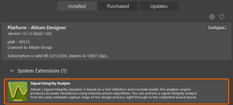
Altium NEXUS includes a signal integrity simulator that can be accessed during both the design capture and board layout phases of the design process, allowing both pre- and post-layout signal integrity analysis to be performed (Tools » Signal Integrity). The signal integrity simulator models the behavior of the routed board by using the calculated characteristic impedance of the traces combined with I/O buffer macro-model information as input for the simulations. The simulator is based on a Fast Reflection and Crosstalk Simulator, which produces very accurate simulations using industry-proven algorithms.
Because both design capture and board design use an integrated component system that links schematic symbols to relevant PCB footprints, SPICE simulation models and signal integrity macro-models, signal integrity analysis can be run at the schematic capture stage prior to the creation of the board design. When no board design is present, the tool allows you to set up the physical characteristics of the design, such as the desired characteristic trace impedance, from within the signal integrity simulator. At this pre-layout stage of the design process, the signal integrity simulator cannot determine the actual length of particular connections so it uses a user-definable average connection length to make its transmission line calculations. By carefully choosing this default length to reflect the dimensions of the intended board, you can gain a fairly accurate picture of the likely signal integrity performance of the design.
Nets with potential reflection problems can be identified and any additional termination components can be added to the schematic before proceeding to board layout. The values of these components can then be further tuned once the post-layout signal integrity analysis has been performed.

The Signal Integrity analysis engine helps identify nets with potential reflection issues. Note that measurements can be taken directly from the waveforms.
► Learn more about Impedance Matching the Components
Defining the High-Speed Signals
Main articles: Defining High-Speed Signal Paths with xSignals, xSignal Wizard
High-speed design is the art of managing the flow of energy from one point on a circuit board to another point. As the designer, you need to be able to focus your attention and apply the design constraints onto a signal that travels from this point on the board to that point on the board. This signal you are focusing on is not necessarily a single PCB net though. The signal might be one branch of A0 in a design that you intend to route in a T-branch topology, with the other branch of A0 being another signal you need to focus your attention on as well, and be able to compare the route lengths of these two signals. Or the signal might include a series termination component in its path (which the PCB editor sees as one component and two PCB nets), and if that signal is in a differential pair, its length needs to be compared to the length of the other signal in that pair.
You can manage these requirements using a feature known as xSignals, where an xSignal is essentially a user-defined signal path. You select the source pad and the target pad (in the workspace or in the PCB panel) then right-click on either to define that signal path as an xSignal. As well as interactively defining an xSignal by its start and end pads, you also can run the intelligent xSignals Wizard, whose heuristics will help you to quickly set up a large number of xSignals between the chosen components. These xSignals can then be used to target design rules to your high-speed signals. The software understands the structure of these xSignals; for example, calculating the overall length of multiple nets connected through a termination component, as well as the distance through that termination component.
The PCB panel includes an xSignal mode that is used to examine and manage the xSignals. The panel also provides feedback on the signal length, highlighting xSignals that are close to meeting (yellow) or failing to meet (red) the applicable design constraints. In the image below the xSignal lengths of the CLK1 differential pair are different in length by more than allowed by the applicable Matched Length design rule. The panel includes the Signal Length, which is an accurate point-to-point length. Traditional length inconsistencies, such as tracks within pads and stacked track segments, are resolved, and accurate via span distances are used to calculate the Signal Length.
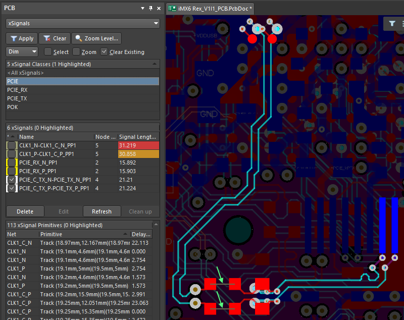
Use the xSignals mode of the PCB panel to manage and investigate your xSignals. Note the thin line; this indicates the signal path through a series component.
(Image courtesy FEDEVEL Open Source, www.fedevel.com)
Defining the Properties of the Routing
Main article: Controlled Impedance Routing
Traditionally, board designers would define the widths and thickness of the routing by entering a dimension for the width and selecting a thickness of copper for that layer. This was generally sufficient since you only needed to ensure that the current could be carried and the required voltage clearances were maintained. This approach is not sufficient for the high-speed signals in your design, for these you need to control the impedance of their routes.
Controlled Impedance routing is all about configuring the dimensions of the routes and the properties of the board materials to deliver a specific impedance. This is done by defining a suitable impedance profile, and then assigning that profile to the critical high-speed nets in the routing design rules.
Defining the Impedance Profile
Main article: Configuring the Layer Stack for Controlled Impedance Routing
Impedance profiles are defined in the PCB editor's Layer Stack Manager (Design » Layer Stack Manager). The Layer Stack Manager opens in a document editor, in the same way as a schematic sheet, the PCB, and other document types do.
Once the layer properties have been configured, switch to the Layer Stack Manager's Impedance tab to add or edit single or differential impedance profiles.
 A 50Ω impedance profile defined for individual nets routed on the top layer, hover the cursor over the image to display the settings for the same profile for layer L3.
Configuring the Design Rules
The routing impedance is determined by the width and height of the route, and the properties of the surrounding dielectric materials. Based on the material properties defined in the Layer Stack Manager, the required routing widths are calculated when each impedance profile is created. Depending on the material properties, the width may change as the routing layer is changed. This requirement to changes widths as you change routing layers is automatically managed by the applicable routing design rule configured in the PCB Rules and Constraints Editor (Design » Rules).
For most board designs, there will be a specific set of nets to be routed with a controlled impedance. A common approach is to create a net class or differential pair class that includes these nets, then create a routing rule that targets this class, as shown in the images below.
Normally you manually define the Min, Max and Preferred Widths, either in the upper constraint settings to apply them to all layers; or individually for each layer in the layer grid. For controlled impedance routing you enable the Use Impedance Profile option instead, then select the required Impedance Profile from the dropdown. When this is done, the Constraints region of the rule will change. The first thing you will notice is that the available layers region of the design rule will no longer show all signal layers in the board, it will now only show the layers enabled in the selected Impedance Profile. The Preferred Width values (and diff pair gap) will update to reflect the widths (and gaps) calculated for each layer. These Preferred values cannot be edited but the Min and Max values can, set these to suitable smaller/larger values.
Routing Width Design Rule
For single-sided nets, the routing width is defined by the Routing Width design rule.
 When you choose to Use an Impedance Profile, the available layers and Preferred Widths are controlled by the selected profile.
Differential Pairs Routing Design Rule
The routing of differential pairs is controlled by the Differential Pair Routing design rule.
 For a differential pair, the available layers, the Preferred Width and the Preferred Gap are controlled by the selected profile.
► Learn more about Differential Pair Routing
Choosing the Impedance
So how do you know what target impedance to select? This is normally driven by the characteristic source impedance of the logic family or technology being used. For example, ECL logic has a 50Ω characteristic impedance, and TTL has a source impedance range of 70Ω to 100Ω. 50Ω to 60Ω is a common target impedance used in many designs, and for differential pairs, 90Ω or 100 Ω differential impedance is common. Remember, the lower the impedance the greater the current drain, the higher the impedance the more chance there will be EMI emitted, and the more susceptible that signal will be to crosstalk.
A 100Ω differential pair can also be viewed as two, 50Ω single-ended routes that have the same length. This is not exactly correct due to the coupling that occurs between the pair, which becomes stronger as they become closer, reducing the differential impedance of the pair. To maintain 100Ω differential impedance the width of each route can be reduced, which slightly increases the characteristic impedance of each route in the pair by a few ohms.
Defining the Properties of the Board
Main article: Layer Stack Management
The materials used for the layers in your board, their dimensions, and the number of and order that the layers are arranged, are all defined in the Layer Stack Manager. Here you configure the various layers that are needed to fabricate the final board including the copper signal and plane layers, the dielectric layers that separate the copper, the cover layers, and the component overlay.

All fabricated layers are defined in the Layer Stack Manager Stackup tab.
Configuring the Vias
Main article: Defining the Via Types
As mentioned in the overview section of this article, vias affect the impedance of the signal routing and are a key consideration in high-speed design. As well as the length, hole diameter, and via land area affecting the impedance that the signal sees, any unused portion of a via barrel can act as a stub, contributing to signal reflections. To manage this, various layer-to-layer via styles can be fabricated, including Blind, Buried, µVia, and Skip Vias. These via types are all supported in Altium NEXUS.
Vias are defined as part of the layer stack, in the Layer Stack Manager's Via Types tab. Back drilling of unused via barrels is also supported, these are defined in the Layer Stack Manager's Back Drills tab (Learn more about configuring the board for back drilling).
 All of the various types of vias that can be fabricated can be defined in the Via Types tab of the Layer Stack Manager.
Quantitative studies have been performed to understand the impact of vias, such as the Altera Application Note AN529 Via Optimization Techniques for High-Speed Channel Designs.
Summarizing this study and other references, the following guidelines are given to help minimize the impact of vias:
- Reduce the size of the via annular ring where the signal route connects to the via, the App Note suggests a via diameter/hole size of 20/10 mil (0.5/0.25 mm) for mechanically drilled vias.
- Remove unused annular rings (also known as NFPs, or Non-Functioning Pads) on layers that the via is not connected to. Use the Tools » Remove Unused Pad Shapes command to do this.
- Increase the clearance from the via barrel to adjacent plane layers. This is controlled by the Power Plane Clearance design rule, the App Note suggests 40 to 50 mil (1.0 to 1.25 mm). Note that this increases the size of blowouts in those plane layers.
- Place stitching vias adjacent to signal vias whenever the signal route has a layer change that results in the return path switching to another layer. If the new reference plane layer is the same voltage as the original reference plane then those planes should be tied together with a via, within 35 mil (0.9 mm) of the signal via (center to center).
- When the signal route has a layer change and the new reference plane layer is a different voltage, place decoupling capacitors adjacent to the signal via. This capacitor decouples directly between the 2 planes, regardless of the voltages they carry. Note that this solution can result in noise being coupled from one plane to the other, so this should only be done as a last resort to reduce the return path loop area.
- Remove via stubs (extra via length beyond the layer that the signal route accesses the via). This is done by using suitable blind and buried vias, or by via back drilling during fabrication.
Managing the Return Path for High-Speed Signals
A good quality return path is essential for each high-speed signal in the design. Whenever the return path deviates and does not flow under the signal route, a loop is created and this loop results in EMI being generated, with the amount being directly related to the area of the loop.
Creating Power Planes
- A power plane can be created from either a plane layer, or a signal layer covered by a polygon(s).
- Creating a power plane with a plane layer:
- Plane layers are added in the Layer Stack Manager, right-click on an existing layer to Insert layer above or Insert layer below to add a new plane layer.
- With the plane layer selected as the active layer, double-click anywhere within the plane to open the Split Plane dialog, where the net can be assigned.
- The software automatically pulls the plane edge back from the edge of the board by the amount specified in the Pullback Distance column for that layer in the Layer Stack Manager. If that column is not visible, right-click on an existing column heading to access the Select Columns command.
- A plane layer can be split into separate regions by placing lines (Place » Line). Press Tab after starting to place the first line segment to set the width of the split line. Place the line segments from board edge to board edge, or create a closed shape for an island. The software will automatically detect the separate shapes created by the split lines, double-click on each shape to assign it to a net.
- Creating a power plane with polygons on a signal layer:
- Signal layers are added in the Layer Stack Manager, right-click on an existing layer to Insert layer above or Insert layer below to add a new signal layer.
- If separate power zones are required it can be easier to cover the entire layer with a polygon and then slice it (Place » Slice Polygon Pour). Press Tab after starting to place the slice line to open the Line Constraints dialog, where you can set the slice width - this width will become the distance between the two polygons created by the slicing action. The slice line must start outside the polygon and finish outside the polygon.
- To repour a polygon, right-click and select Polygon Actions » Repour Selected from the context menu.
- Polygons can also be shelved (temporarily hidden), right-click and select the relevant command from the Polygon Actions sub-menu. Use this feature when you need to move components and routing.
- It can help to display the different nets in a different color, as shown in the images below. This can be done in the schematic or the PCB, learn more about Applying Color to the Nets.

 The first image is a plane layer split into 3v3 and 5v0 zones; the second image is a signal layer with a 3v3 polygon and a 5v0 polygon. Net colors have been assigned and highlighting enabled.
The Plane as a Signal Return Path
A good quality return path is one where:
- There are no breaks, splits, or blowouts (holes in the plane created by a via or thruhole pin) under the signal route in the plane providing the return path (the plane closest to the signal of interest).
- The width of the return path is ideally 3x the width of the signal routing, or 3x the distance from the route to the plane, whichever is smaller. While the greatest current density is directly below the signal route, it also spreads out into the plane on either side of the route with approximately 95% flowing within 3x the route width. Breaks in the plane within this region have the effect of increasing the impedance of the return path, and any deviation in the return path will create a loop. In terms of signal integrity, this increased return path impedance impacts the quality of the signal as much as increasing the impedance of the signal path.
- The area of the loop has been minimized. Generally, it is more important to reduce the loop area than minimize the routed signal length. If the return path encounters a blowout, consider re-routing the signal to suit an available return path.
- When a power plane is providing the return path, the return energy will ultimately get to ground through a decoupling capacitor. Carefully consider the location of the decoupling capacitors near the source pin of the signal to minimize the size of any loop created.
Managing Split and Multiple Power and Ground Planes
There is general agreement that a ground plane should not be split unless there is a specific requirement for it and you understand how to define and manage it. Instead, the components should be arranged to keep noisy components separate from quiet components, and to also cluster components by the supply rail that they use.
Other points to keep in mind about power and ground planes include:
- If the design requires a ground plane to be partially split then signals that traverse those areas should be routed across the bridge (the zone without a split below it).
- If you are attempting to minimize circuit noise, it is better to use additional ground planes than to split a plane, and where possible, include plane layers for both the supply and ground rails of each regulated power supply.
- If the design includes multiple rails with each distributed on its own plane, ensure that each power plane only references its own ground plane. Do not let allow a power plane overlap (reference) a different rail's ground plane. This creates capacitive coupling, allowing noise to travel from one supply to another.
- If the adjacent plane is a power plane that must be split into different voltage areas, then you might need to decouple directly across the two voltages areas to provide a suitable return path.
Visualizing Split Planes
To help with the task of visually checking the return paths, you can configure the display so you can more easily examine the return path under the critical route paths.
Checking if signals travel over a split line as they traverse different voltage areas on the plane. The four highlighted nets
cross a split in the VCC power plane, creating a split in the return path of those signals.
To do this:
- Assign a color to each power net, learn more about Applying Color to the Nets.
- Reduce the display of layers to only show the relevant signal and plane layers. This set of layers can be saved as a Layer Set, learn more about creating a layer set.
- Switch to the signal layer and Ctrl+Click on the net of interest to highlight it (include Shift as you click to highlight multiple nets). The advantage of highlighting over selecting is that highlighting is persistent so they will remain highlighted if you click somewhere else, press Shift+C to clear the current highlight set.
- Highlighting is achieved by dimming the rest of the objects in the workspace, the Dimmed Objects level is set in the Mask and Dim Settings section of the View Configuration panel.
- Make the plane layer the active layer.
Your net(s) will stand out, and any splits or discontinuities that lie in the return path, such as split lines or blowouts created by through-hole pads and vias, will be easier to see.
Detecting Breaks in the Return Path
Breaks or necks in the return path can be detected by the Return Path design rule. The Return Path design rule checks for a continuous signal return path on the designated reference layer(s) above or below the signal(s) targeted by the rule. The return path can be created from fills, regions, and polygon pours placed on the reference signal layer, or it can be a plane layer.
The return path layers are the reference layers defined in the Impedance Profile selected in the Return Path design rule. These layers are checked to ensure the specified Minimum Gap (width beyond the signal edge) exists along the signal's path. Add a new Return Path design rule in the High Speed rule category.
 is defined by the Minimum Gap.") The return path layers are defined in the selected Impedance Profile, the path width (beyond the signal edge) is defined by the Minimum Gap.
The return path layers are defined in the selected Impedance Profile, the path width (beyond the signal edge) is defined by the Minimum Gap.
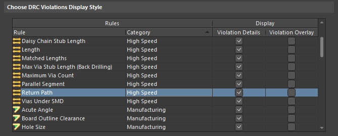
The image below shows return path errors detected for the signal, NetX, with a Minimum Gap setting of 0.1mm. It can be easier to locate Return Path errors by configuring the DRC Violation Display Style to show Violation Details but not the Violation Overlay ( show image), in the Preferences dialog. Doing this highlights the exact locations where the rule has failed, rather than the entire object(s) in violation.
 show image
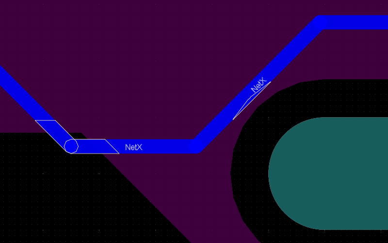
Configuring and Routing Differential Pairs
Main articles: Differential Pair Routing, Controlled Impedance Routing
The definition of differential pairs can be done during schematic capture, or they can be defined once the design has been transferred to board layout. A core requirement of defining a pair on the schematic is to include an _P or _N at the end of the Net name for each of the relevant nets. Differential pairs are identified on the schematic by placing a Differential Pair directive on each net, or by placing one on a Blanket directive, where the Blanket directive overlays a set of enclosed differential-style Net Labels, as shown in the image below.

A Blanket can be used to configure multiple nets as differential pair members.
Working with Differential Pairs:
- In the PCB editor, differential pairs can be defined in the Differential Pair Editor mode of the PCB panel. To simplify the process of defining design rules that apply to the differential pairs, they can either be assigned to Net Classes or to Differential Pair Classes, both of which are defined in the Object Class Explorer.
- To route a differential pair with a controlled impedance, create an impedance profile in the Layer Stack Manager. Learn more about Controlled Impedance Routing.
- The properties of the differential pair routing is defined by the Differential Pair Routing design rule.
- To route a differential pair, you use the Interactive Differential Pair routing command. Click on either the
_Por_Npad to commence routing, then use the Spacebar to cycle through the available exit routing shapes. The routing behavior is the same as single net routing, press Shift+F1 for a list of interactive routing shortcuts. As you approach the target pads, press Ctrl+Click to complete the routing up to the pads.
Differential Pair rules of thumb:
- Length matching is critical for differential pairs to be effective, keep the lengths matched to within 25 mil (0.635 mm). Another rule of thumb that is used is to match the lengths to be within 20% of the signal rise time. Differential pairs work because the return energy flows back through the other member of the pair, the more that the lengths do not match, the greater the amount of energy that returns through the nearest plane layer instead.
- Discontinuities in the coupling, such as when the pair members route around either side of an obstacle, increases the impedance. It can be better to route the entire pair with looser coupling (for example 2 x signal route width) to reduce the amount that the impedance changes due to coupling discontinuities.
- Keep aggressor routes away, especially on surface layers, aim for a clearance of 3 x the signal route width for potential aggressor nets.
- As a general rule, aim for a pair-to-other signal clearance of 2 x signal route width.
- Keep same-layer ground polygons away by at least 3 x signal route width.
- Reflections introduced by vias and coupling discontinuities are managed through controlled impedance routing, doing this requires a continuous reference plane below the signal path.
- Reduce the signal layer-to-plane separation to improve immunity to crosstalk.
Controlling and Tuning the Route Lengths
Main articles: Length Tuning, Length design rule, Matched Length design rule
A key requirement of managing high-speed signals on a board is to control and tune their route lengths.
- The absolute lengths can be monitored by the Length design rule, and the and relative route lengths monitored by the Matched Length design rule.
- The current lengths of a set of nets, and their compliance with applicable design rules, can be checked in the PCB panel in Nets mode (as shown below).
- If there is a Length rule and/or a Matched Length rule defined, then you can monitor the length during interactive routing or length tuning by displaying the Length Tuning Gauge (Shift+G).
-
The delay caused by the length of the pin within the device package is supported, to learn more read about Pin Package Delay.
-
Nets that include serial components in their path are managed by defining xSignals.
Design Rules
- Managing the Overall Route Lengths - the overall route length of a net or set of nets can be monitored by a Length design rule. The Length design rule has a minimum and maximum allowed length, if the Signal Length is less than the allowed minimum it is highlighted in yellow in the PCB panel (in Nets mode), a Signal Length greater than the allowed maximum is highlighted in red.
- Managing the Relative Route Lengths - the relative route lengths of a set of nets can be monitored by a Matched Length design rule. The Matched Length design rule has a tolerance and uses the longest route in the set of targeted nets as reference length. Yellow highlighting of the Signal Length in the panel indicates that the length of this signal is less than the longest route length minus the tolerance. Red highlighting indicates that this signal's length is greater than the longest route length.
To understand how the settings of these two rules are resolved when both are present in a design, refer to the Length Tuning page.
Monitoring the Route Length
Current route lengths are displayed in the Nets mode of the PCB panel, and are updated as you route. The Routed length value will go yellow as you approach the target length, and turn red if you exceed it.
If there is a Length rule and/or a Matched Length rule defined, you can monitor the length during interactive routing or length tuning by displaying the Length Tuning Gauge. While you are routing, use the Shift+G shortcut to toggle the Gauge on and off.
The Gauge shows the current Routed Length as a number over the top of the slider, while the slider shows the Estimated Length. During length tuning the Estimated Length = Current Routed Length; if you are using the Gauge during interactive routing then the Estimated Length = Routed Length + distance to target (length of connection line).
 The Gauge settings are calculated from the constraints defined by the applicable rules.
- Gauge minimum (left edge of gauge) is 45 (lowest
MinLimit) - Gauge maximum (right edge of gauge) is 48 (highest
MaxLimit) - Left yellow bar (highest
MinLimit) is 46.58 - Right yellow bar (lowest
MaxLimit) is 47.58 (obscured by the green bar in the image above) - Green bar (
TargetLength) is 47.58 (route length of the longest net in the set, equal toMaxLimit) - Green slider and the overlaid numerical value (Current route length) is 47.197.
Tuning the Route Lengths
Route lengths can be tuned after the routing is complete, using the Interactive Length Tuning command, or the Interactive Diff Pair Length Tuning command (Route menu). These commands add accordion sections to the routing, in a choice of three shapes.
If there is an applicable Length rule and Matched Length rule, the length tuning tool considers both of these rules and works out the tightest set of constraints. So if the maximum length specified by the Length rule is shorter than the longest length targeted by the Match Length rule, then the Length rule wins and its length is used during tuning.
To see which rules are being applied or to change the accordion properties during length tuning, press Tab to open the Interactive Length Tuning mode of the Properties panel, as shown below. Note the Target Length, this is the Max Limit of the strictest applicable rule settings.
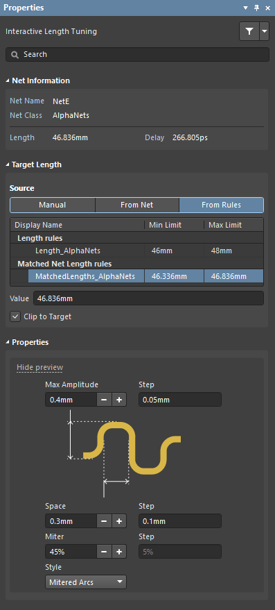
Press TAB during length tuning to open the panel in Interactive Length Tuning mode,
where you can select the target length mode and adjust the accordion parameters.
To tune the length of a net, run the command and then click anywhere along the net's length. Move the cursor so that it follows the path of the route, tuning accordion sections will be added as you do. Tuning sections will continue to be added until the length requirements defined by the applicable design rule(s) have been satisfied. If the cursor moves outside the bounds of the tuning accordions, the accordion shapes will disappear - when the cursor is moved so that it is back within the bounds of the accordion shape, they will re-appear.
► Learn more about Length Tuning
In Conclusion
While it is not possible to derive a universal set of rules that apply to every high-speed design, it is possible to follow good design practices that will help you succeed with your high-speed design. There are a number of industry experts that deliver practical and popular training courses on high-speed design. Use the links below to learn more, and to research specialized training options.
References
The author gratefully acknowledges the work of the following industry experts, this article is an attempt to summarize their collective knowledge.
- Microstrip Propagation Times
- Splitting Planes For Speed and Power
- Skin Effect
- Differential Trace Design Rules - Truth vs Fiction
- Via Inductance
- 10 Layer Stack
Lee W. Ritchey books and articles
- Right the First Time
- A Treatment of Differential Signaling and its Design Requirements
- PCB laminates influence high-speed data rates, Part 1, Part 2
In-Circuit Design articles - Barry Olney
- Differential Pair Routing
- The Plain Truth About Plane Jumpers
- Critical Placement
- Stackup Planning (Parts 1, 2 & 3)
- The Perfect Stackup
Best Practice in Circuit Board Design - Tim Jarvis RadioCAD Limited
PCB Layout - Learn EMC website
Keith Armstrong articles, EMC Information Centre (free registration required)
The Electronic Packaging Handbook - Glenn R. Blackwell
The Printed Circuits Handbook - Clyde Coombs and Happy Holden
The HDI Handbook - Happy Holden and others
Via Optimization Techniques for High-Speed Channel Designs - Altera Application Note AN529
High-Speed PCB Design Considerations - Lattice Semiconductor Application Note TN 1033
Measuring a Signal's Flight Time - Chris Grachanen, EDN
The Future of HDI Via Structures, Power Delivery, and Thermal Management in Next Generation Printed Circuits - Tom Buck TTM Technologies