
Design View
This document is no longer available beyond version 4. Information can now be found here: Design View for version 5
Parent page: PCB Design Objects

Place a Design View to show a specific area of the board. This example has been scaled to 200%.
Summary
The PCB Design View object is a graphic snapshot of any rectangular-shaped region of the current board or another board. It can be placed anywhere in the design space and scaled to any size.
Availability
A Design View can be placed in the PCB Editor in one of the following ways:
- Click Place » Design View from the main menus.
- Right-click in the design space then choose Place » Design View from the context menu.
Placement
After launching the command, a design view will appear attached to the cursor. Position the design view in a suitable location then click or press Enter to place it.
Additional actions that can be performed during placement while the design view is still floating on the cursor and before the design view is anchored are:
- Press the Tab key to pause the placement to access the Design View mode of the Properties panel from where its properties can be changed on the fly. Click the design space pause button overlay (
 ) to resume placement.
 - Press the Alt key to constrain the direction of movement to the horizontal or vertical axis, depending on the initial direction of movement.
After placement of the design view, you can define the display of desired layers by performing the following steps:
- With the Design View selected in the design space, open the Properties panel by double-clicking or right-clicking then choosing Properties from the context menu.
- Use the Define button in the Properties panel to interactively define the area of interest.
- In the Layers section of the Properties panel, click (toggle) the
 icon to enable the display of the desired layers. When enabled in the Properties panel, the desired layer(s) will display the
  icon.
icon.
Including a Design View in Printed or PDF Output
Design Views are included in printed and PDF output. The Design View retains its own layer visibility settings in the output allowing it to present as required in the printed/PDF output. Note that the primitives on layers used in the Design View continue to obey the display settings defined for that layer in the Print dialog. For example, if the Top Overlay is displayed in the Design View and the Top Overlay is configured to display tracks in Draft mode for that output in the Output Job, then the Top Overlay tracks in the Design View will also present in Draft mode.
Graphical Editing
Once a Design View has been placed in the design space, you can interactively adjust the position, scale, size and focus of the View.
- Change the position – Click+Drag the Design View object to a new location on the PCB design space.
- Adjusting the Scale – click once to select the Design View then Click+Drag on a corner handle to scale the Design View up (drag out) or down (drag in).
- Adjusting the View Size – click once to select the Design View then Ctrl+Click+Drag on a corner handle to resize the Design View.
- Changing the Focus – Ctrl+Click+Drag anywhere within the Design View to slide the currently viewed area around within the Design View window.

Ctrl+Click+Drag to slide and adjust the area currently being viewed in the Design View.
Non-Graphical Editing
The following methods of non-graphical editing are available.
Editing via Design View Dialog or Properties Panel
Properties page: Design View Properties
This method of editing uses the associated Design View dialog and Properties panel mode to modify the properties of a Design View object.
 and the Design View mode of the Properties panel (the second image)")
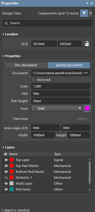
The Design View dialog (the first image) and the Design View mode of the Properties panel (the second image)
During placement, the Design View mode of the Properties panel can be accessed by pressing the Tab key. Once the Design View is placed, all options appear.
After placement, the Design View dialog can be accessed by:
- Double-clicking on the placed Design View object.
- Placing the cursor over the Design View object, right-clicking then choosing Properties from the context menu.
After placement, the Design View mode of the Properties panel can be accessed in one of the following ways:
- If the Properties panel is already active, select the Design View object.
- After selecting the Design View object, select the Properties panel from the Panels button at the bottom right of the design space or select View » Panels » Properties from the main menus.
Editing Multiple Objects
The Properties panel supports editing multiple objects, where the property settings that are identical in all currently selected objects may be modified. When multiples of the same object type are selected manually, via the Find Similar Objects dialog or through a Filter or List panel, a Properties panel field entry can be edited for all selected objects. If values of a property are different for objects in the selection, the appropriate field will be shown as an asterisk (*) – a new property value will be applied to all selected objects.
Editing via a List Panel
Panel pages: PCB List, PCB Filter
A List panel allows you to display design objects from one or more documents in tabular format, enabling quick inspection and modification of object attributes. Used in conjunction with appropriate filtering – by using the applicable Filter panel, or the Find Similar Objects dialog – it enables the display of just those objects falling under the scope of the active filter – allowing you to target and edit multiple design objects with greater accuracy and efficiency.