
Power Analyzer от Keysight
Практическая эффективность топологии (layout) печатной платы зависит от множества факторов, многие из которых можно с достаточной точностью предсказать с помощью различных инструментов анализа PCB, например посттопологического анализа целостности сигнала. Однако часто упускают из виду — или просто сводят к подходу «по эмпирическому правилу» — разработку наиболее эффективной топологии для систем распределения питания постоянного тока на плате. Речь о том, как проектируются медные области платы, которые обеспечивают как шины питания DC для схемы, так и их «землю»/общий обратный путь к источнику питания. Желаемый результат — эффективная конструкция, сохраняющая целостность DC-разводки питания в проекте.
В современных цифровых устройствах с высокоскоростными цепями, множеством микросхем, высокой плотностью монтажа и несколькими шинами питания требования к сети распределения питания постоянного тока (DC power distribution network) требуют более аналитического подхода. DC-анализ сети питания Power Delivery Network (PDN), или результаты анализа DC Power Integrity (PI-DC), по сути направлены на то, чтобы убедиться: на пути от источников напряжения к нагрузкам предусмотрено достаточное количество меди — другими словами, что полигоны/плоскости, дорожки и переходные отверстия на плате имеют достаточные размеры (и характеристики), чтобы удовлетворить требованиям по потреблению мощности устройств на плате.
К счастью, от «угадывания» при оценке сети питания PCB можно уйти, используя инструмент моделирования DC Power Integrity (PI-DC), который анализирует DC-поведение платы на основе её электрических и физических свойств и помогает инженеру ответить на ключевые вопросы проектирования, включая:
-
Выявить и устранить проблемы с DC-напряжением и плотностью тока.
-
Рассчитать взаимодействия между несколькими сетями и обратными путями.
-
Визуализировать распределение напряжения и плотности тока и выявить «горячие точки» в редакторе PCB.
-
Проверить напряжение, плотность тока и ток через переходные отверстия в любой точке платы.
-
Сформировать отчёт по результатам моделирования анализа.
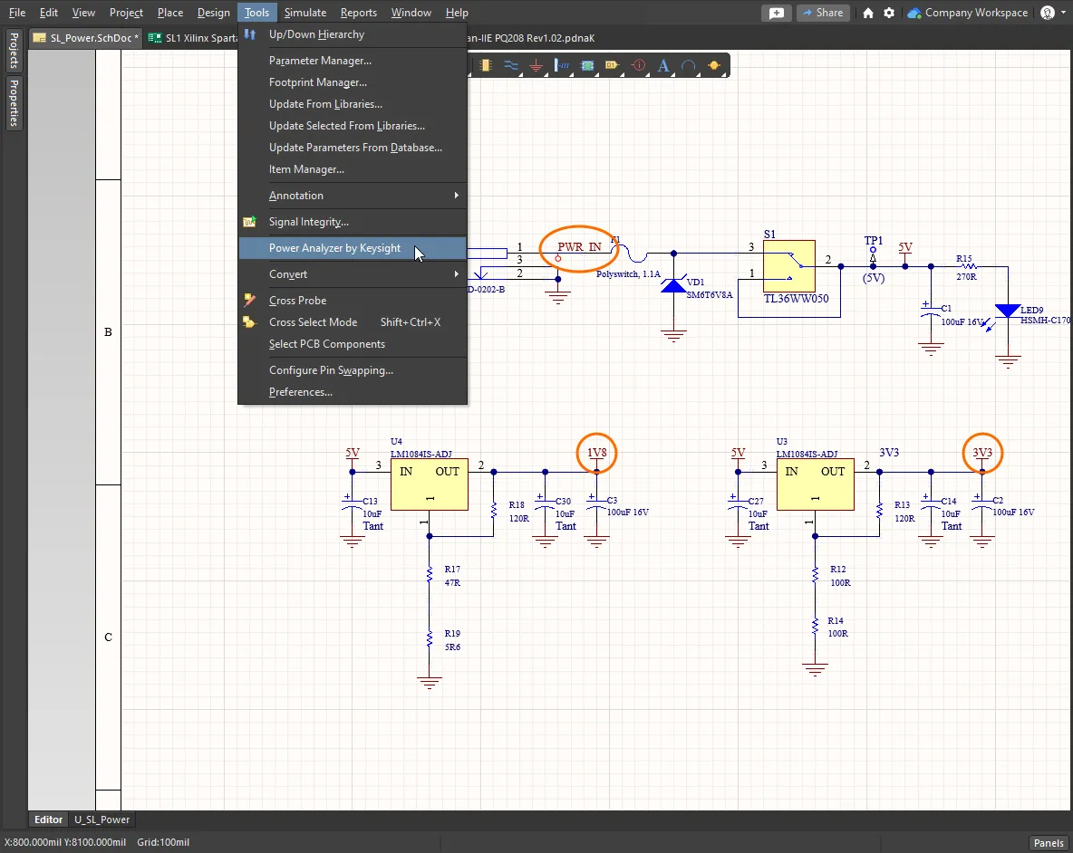
Чтобы выполнять анализ DC Power Integrity прямо в среде проектирования PCB Altium Designer, основным решением является Power Analyzer by Keysight.
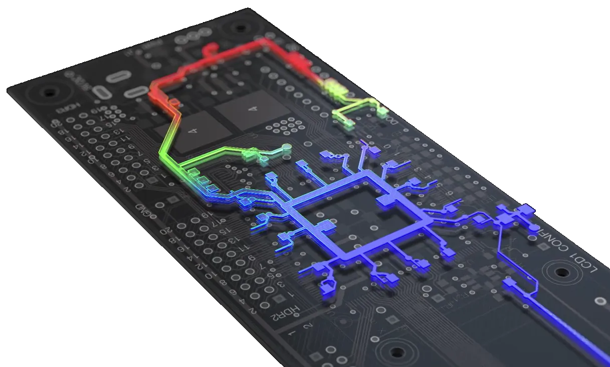
Power Analyzer by Keysight, работающий на базе Keysight Technologies, интегрируется напрямую с Altium Designer и позволяет выполнять PI-DC моделирование и анализ текущего PCB-проекта. Вместо того чтобы полагаться на простые расчёты по площади поперечного сечения для определения токонесущей способности сети питания, Power Analyzer сначала точно моделирует медные структуры, а затем рассчитывает напряжения и токи распределения питания по всей PCB. Представляя результаты в визуальном и табличном виде, инструмент даёт инженеру обратную связь, позволяя быстро скорректировать ширины дорожек, толщины меди и параметры переходных отверстий так, чтобы обеспечить требуемую для проекта целостность DC-питания.
Чтобы выполнить анализ Power Integrity в Altium, инженер сначала создаёт иерархическую сеть всей системы распределения питания, определяя каждую сеть питания и возврата, источники и нагрузки, а также любые последовательные элементы, присутствующие в каждом участке сети питания. После определения сети и настроек конфигурации Power Analyzer может проанализировать всю сеть целиком.
Настройка сети питания
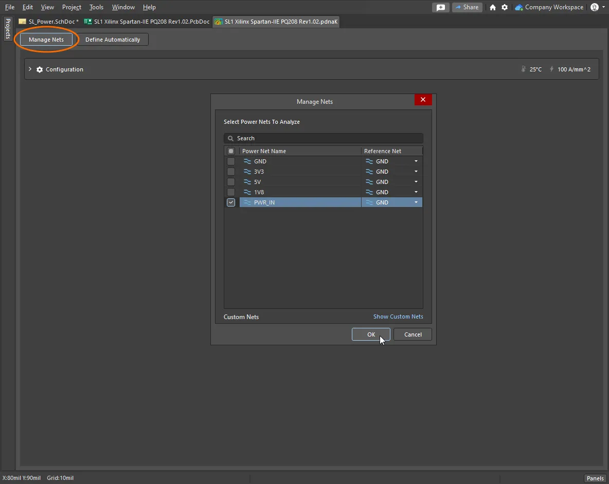
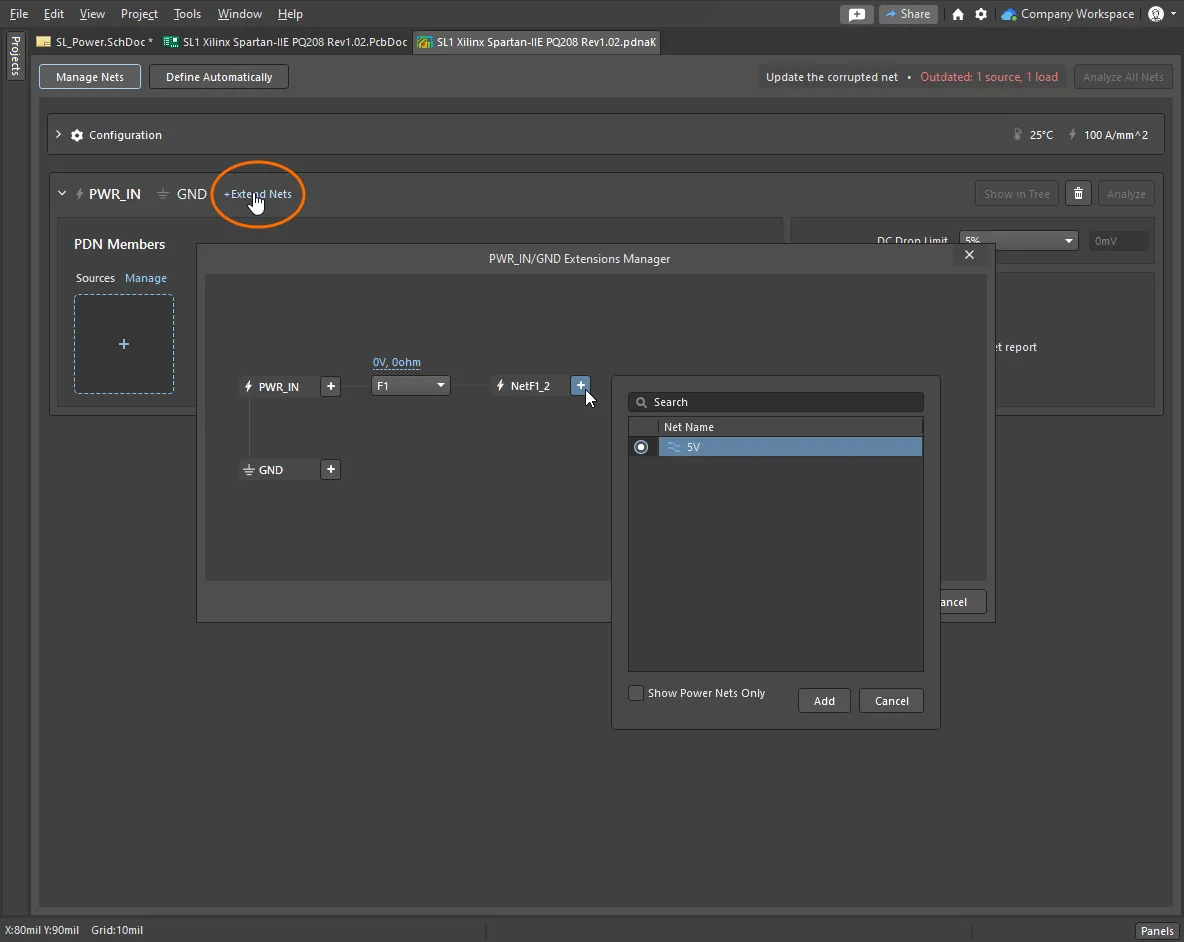
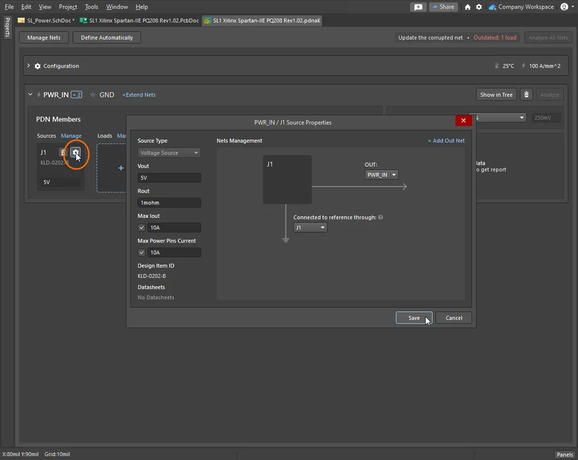
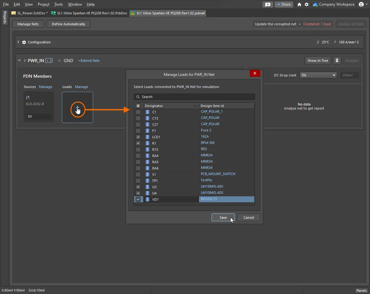
Power Analyzer исследует поток энергии по медным проводящим путям в сети питания. Сеть питания определяется путём идентификации и настройки различных элементов сети, включая сеть (net), источник (source), любые последовательные компоненты и нагрузки (loads). Чтобы настроить сеть питания:
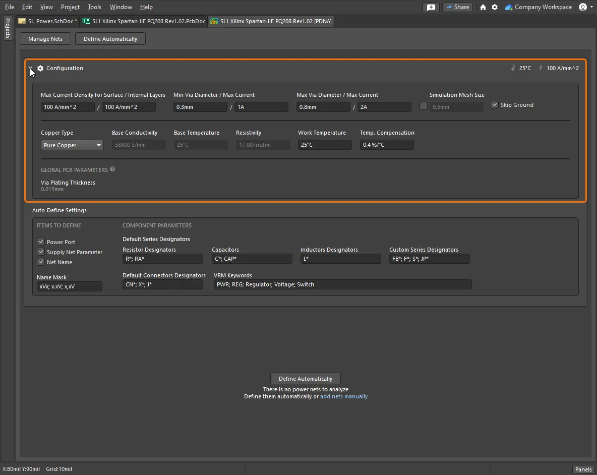
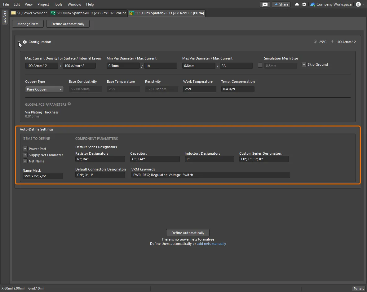
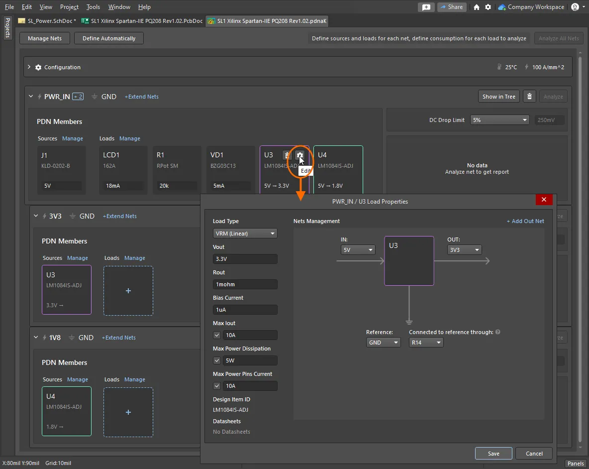
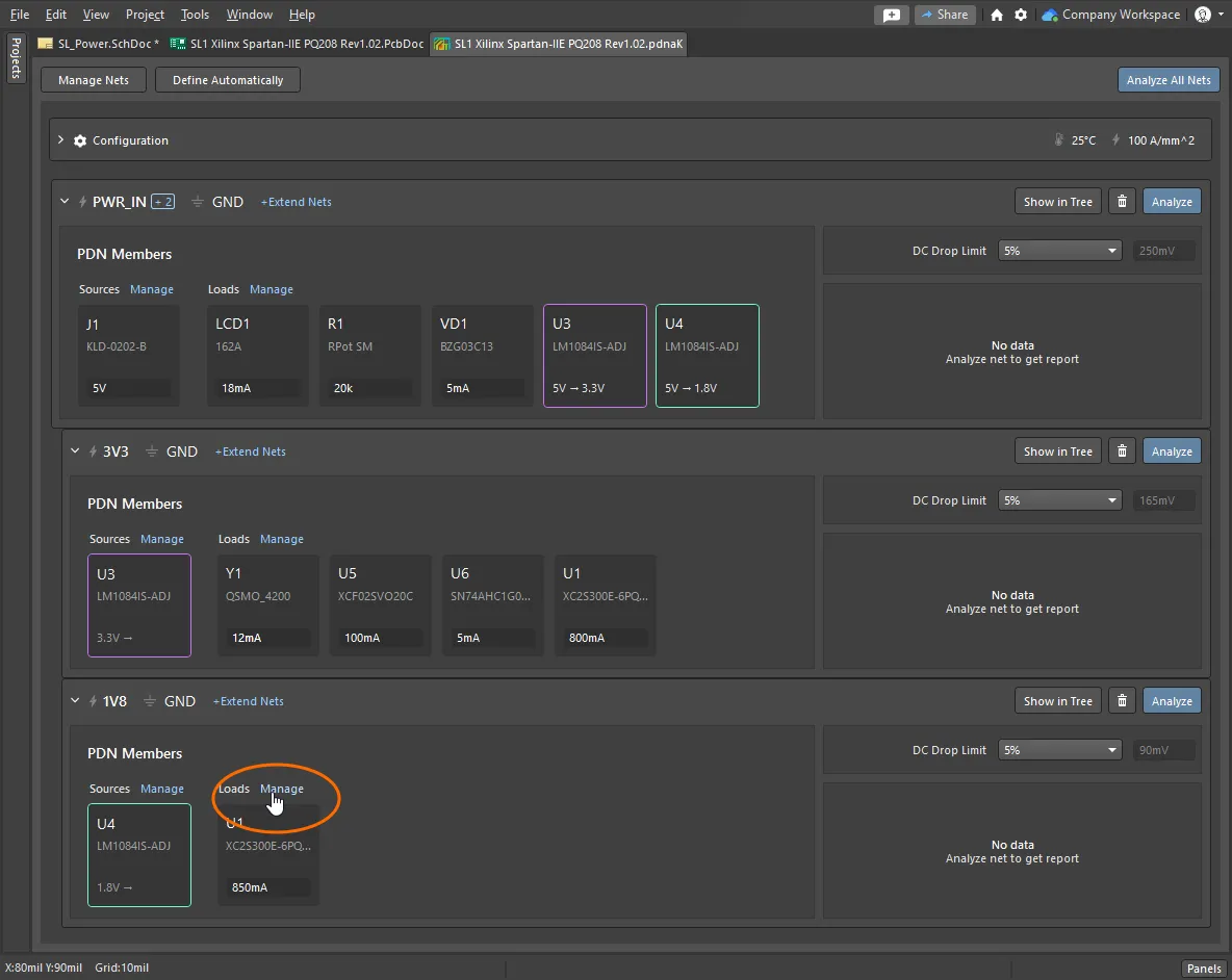
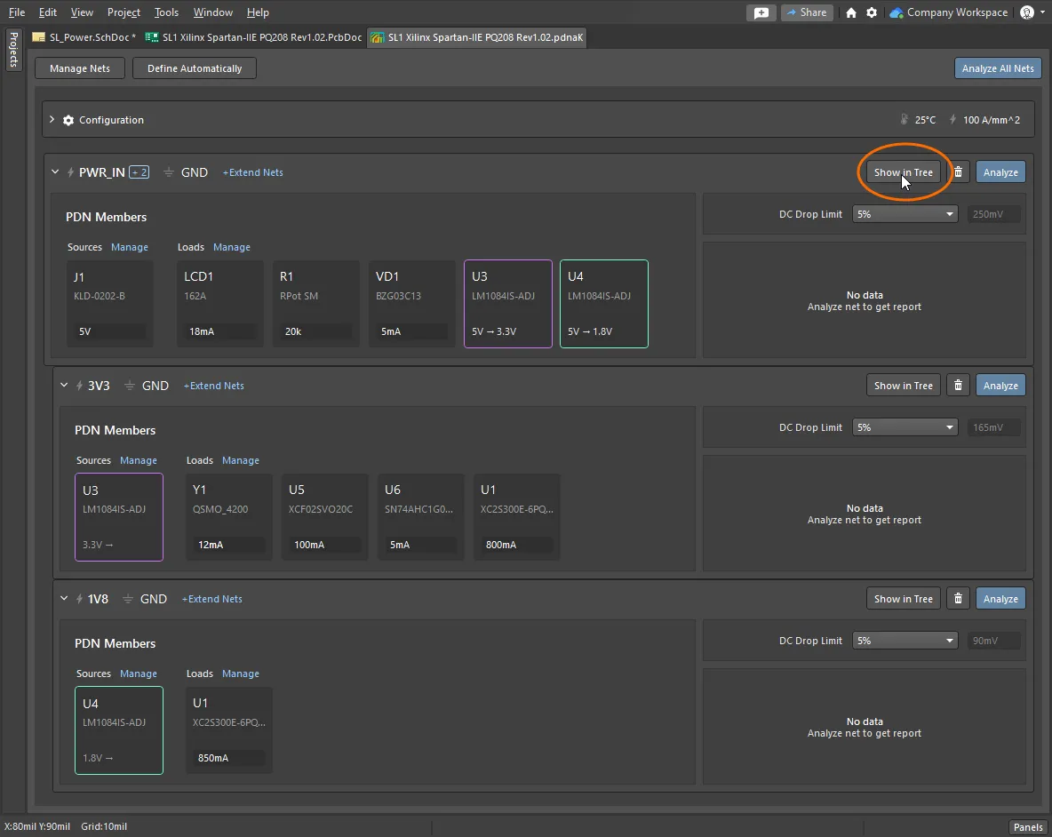
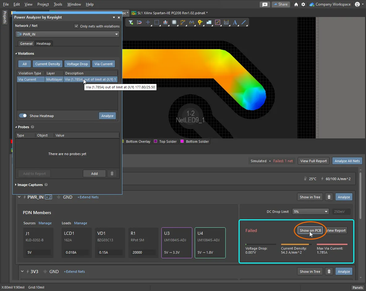
Добавьте документ Analysis в проектАнализ настраивается и запускается из документа Power Analyzer by Keysight ( Настройте свойства платыPower Analyzer необходимо знать физические свойства платы, такие как допустимая плотность тока, тип меди, рабочая температура и т. п. Убедитесь, что значения по умолчанию, заданные в разделе Configuration документа analyzer , подходят для вашего проекта. Автоматическая идентификация сетей питанияPower Analyzer может попытаться определить сети питания автоматически. Для этого ему нужно знать, как распознавать элементы схемы, такие как стабилизаторы напряжения, разъёмы и последовательные компоненты. Помимо использования подсказок вроде префиксов обозначений компонентов, вы также можете добавлять параметры к некоторым компонентам, чтобы улучшить процесс автоматического обнаружения. Подробнее: Configuring the Auto-Define Settings. Выберите сеть(и) питанияНажмите Расширьте сеть(и)Если сеть питания проходит через последовательный компонент, например предохранитель, расширьте сеть и укажите последовательные компоненты и связанные (chained) сети. Подробнее: extending a net. Определите и настройте источникКаждая сеть питания начинается от источника (Source), например разъёма. Включите источник в диалоге Add Source, затем нажмите значок шестерёнки, чтобы настроить этот источник. Подробнее: identifying and configuring the Source. Определите нагрузкиНачните с основных потребителей тока, включая модули стабилизаторов напряжения Voltage Regulator Modules (VRMs). Подробнее: identifying the Loads. Настройте нагрузки и VRMНажмите значок шестерёнки, чтобы открыть диалог Load Properties, и настройте каждую нагрузку. Когда устройство настроено как Voltage Regulator Module (VRM), в иерархии автоматически создаётся дочерняя сеть питания, где этот VRM выступает источником. Определите нагрузки в дочерних сетях питанияУбедитесь, что основные компоненты-нагрузки включены в каждую сеть питания. Подтвердите сеть питанияНажмите кнопку Готово к анализуПроверьте дерево (Tree), чтобы визуально убедиться, что каждая сеть питания завершена. Чтобы перейти от одной сети питания к другой, нажмите ссылку Power Analyzer by Keysight, чтобы вернуться к документу сети питания, и выберите Tree для каждой сети питания. Когда это сделано, можно анализировать сеть питания. |
Анализ сети питания
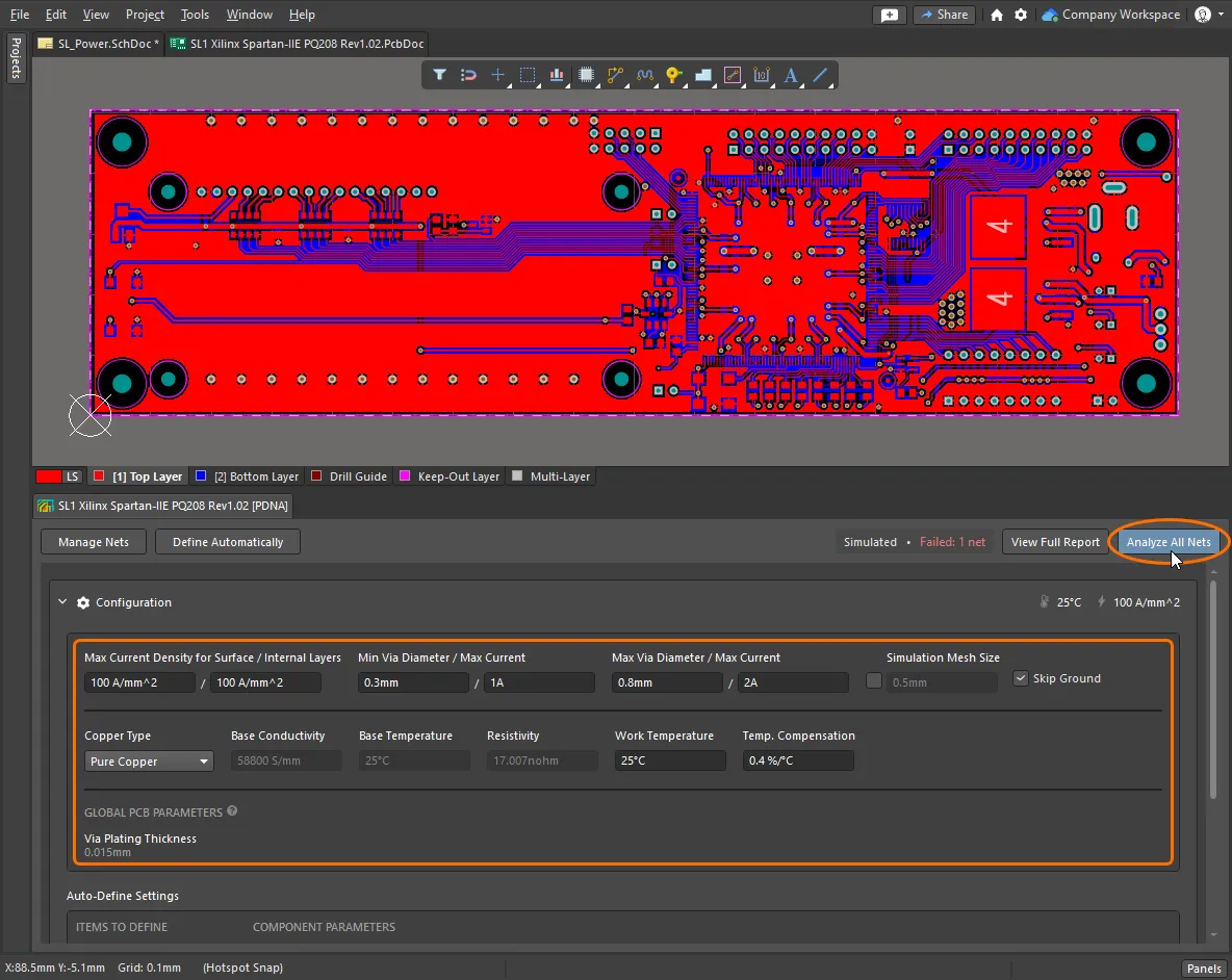
После определения Power Networks вы готовы анализировать распределение DC-питания по плате и через её слои.
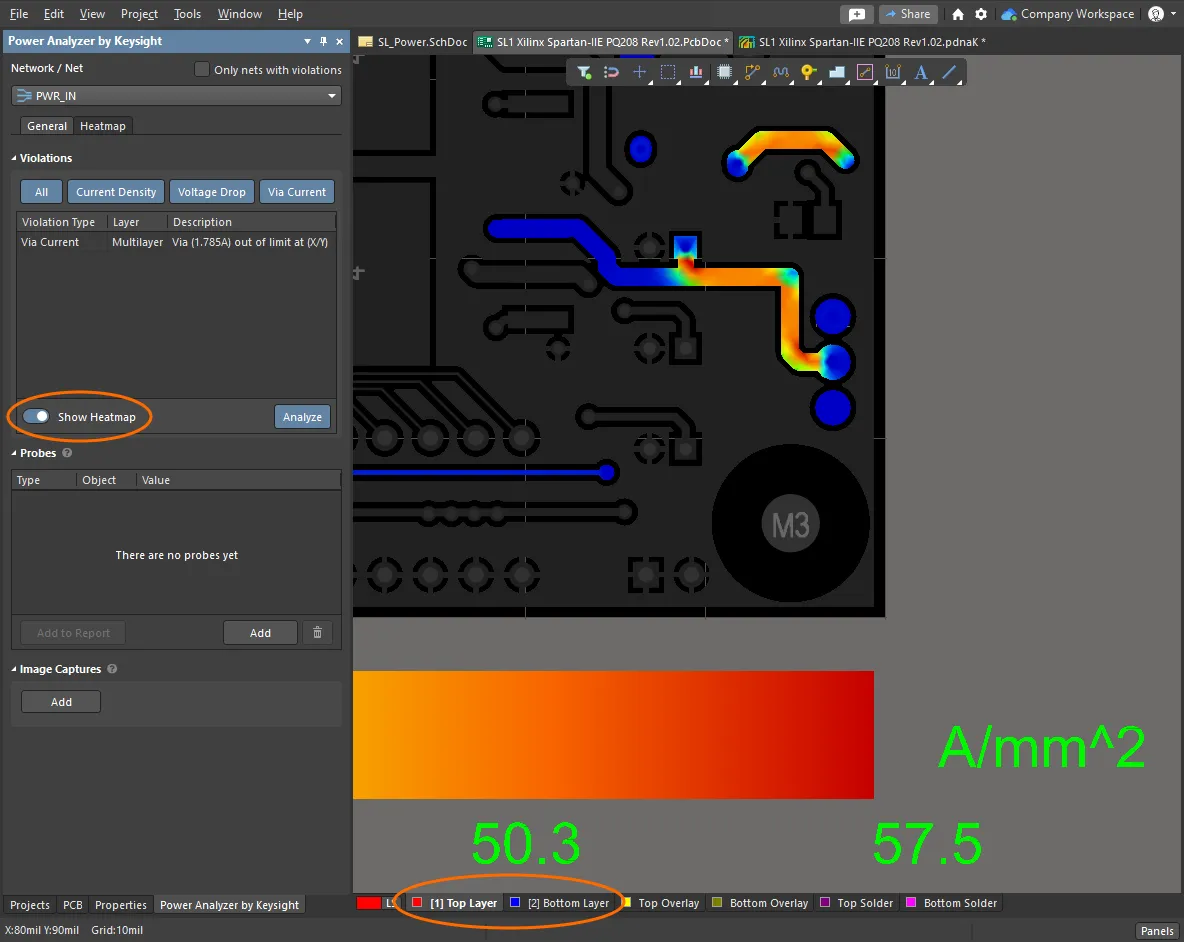
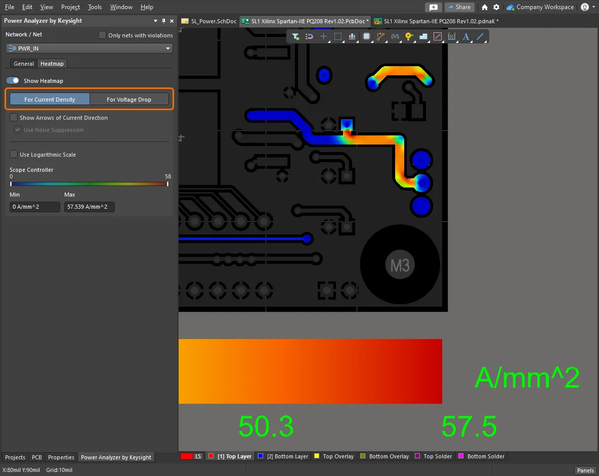
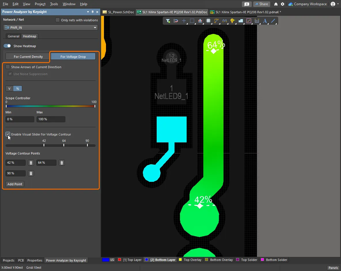
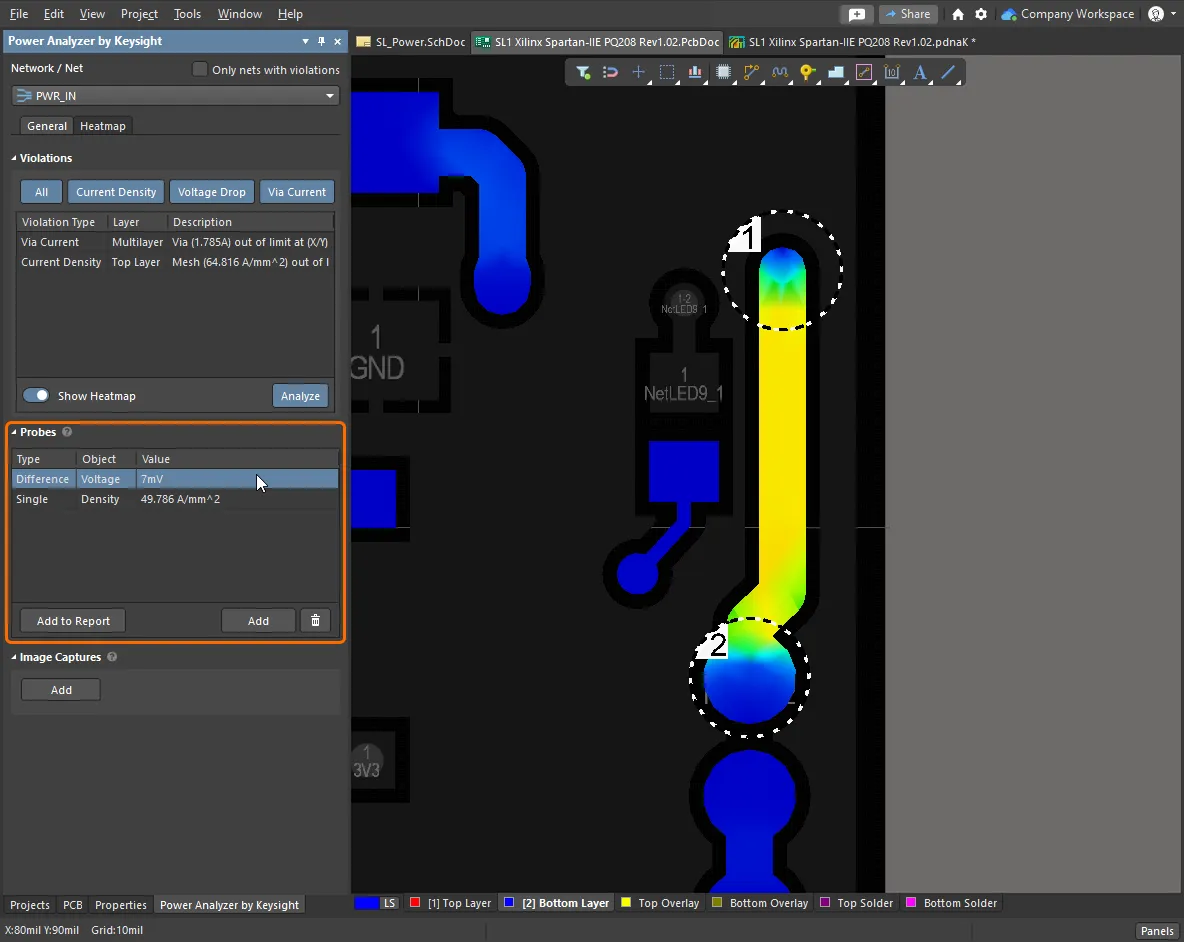
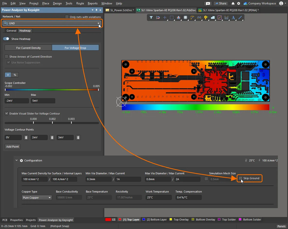
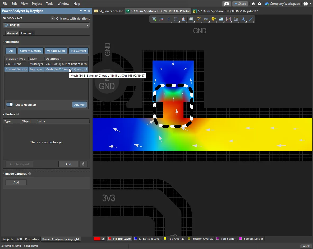
Проанализируйте медные структурыНа основе настроек Configuration, когда вы нажимаете кнопку Показать на PCBСводка результатов анализа Voltage Drop, Current Density и Max Via Current отображается как часть Power Net Definition в документе Изучите тепловые картыРассчитанные токи и падения напряжения отображаются в виде тепловых карт (Heatmaps) прямо в редакторе PCB. Используйте вкладки слоёв редактора PCB, чтобы просмотреть heatmap на каждом слое, переключайтесь между режимами 2D и 3D стандартными сочетаниями 2 и 3 и нажмите кнопку Show Heatmap на панели Power Analyzer by Keysight, чтобы переключаться между тепловыми картами анализа питания и стандартными режимами отображения PCB. Изучите результаты анализаВ редакторе PCB результат анализа сети питания, который вы просматриваете, управляется через панель Power Analyzer by Keysight. В верхней части панели выберите сеть питания/нет, heatmap которого нужно отобразить. Обратите внимание: если в проекте есть нарушения (violations), по умолчанию в выпадающем списке включён пункт Only nets with violations; снимите этот флажок, чтобы включить в список все сети питания. Подробнее о панели Power Analyzer by Keysight Panel. Переключение между плотностью тока и падением напряженияТепловая карта (Heatmap) отображает либо Current Density через медь, либо Voltage Drop по меди; используйте кнопки в верхней части вкладки Heatmap панели, чтобы выбрать нужный режим. Шкала для Heatmap отображается под платой и автоматически масштабируется: для тока — от Zero до Max Current Density, либо для падения напряжения — от (Voltage - VDrop) до Voltage. На Heatmap можно отображать направленные стрелки, показывающие направление протекания тока, а также настраивать шкалу плотности тока или падения напряжения. Подробнее см. настройка и управление отображением Heatmap. Исследование падения напряженияРасположение «горячих точек» плотности тока можно напрямую определить по их цвету на тепловой карте. Поскольку падение напряжения вычисляется как разность между точками, его интерпретация требует более глубокого анализа. Чтобы упростить поиск критических мест, используйте параметр Enable Visual Slider for Voltage Contour для отображения предопределённых контурных линий — либо в вольтах, либо в процентах. Подробнее см. Heatmap для падения напряжения. Зондирование результатовЧтобы снять измерение непосредственно с Heatmap, установите Probe (зонд). Установите один Probe, чтобы отобразить абсолютное значение тока или напряжения в этой точке, либо щёлкните во второй точке, чтобы измерить разницу между двумя точками Probe. Тип измерения (V или I) определяется текущим режимом Heatmap (плотность тока или падение напряжения). Обратите внимание: зондирование центральной точки металлизированного отверстия (thru-hole) всегда будет отображать плотность тока. Подробнее см. Probes. Просмотр результатов для цепи земли (Ground Net)По умолчанию цепь земли (Ground) исключена из результатов Heatmap. Снимите флажок Skip Ground в разделе Configuration документа |

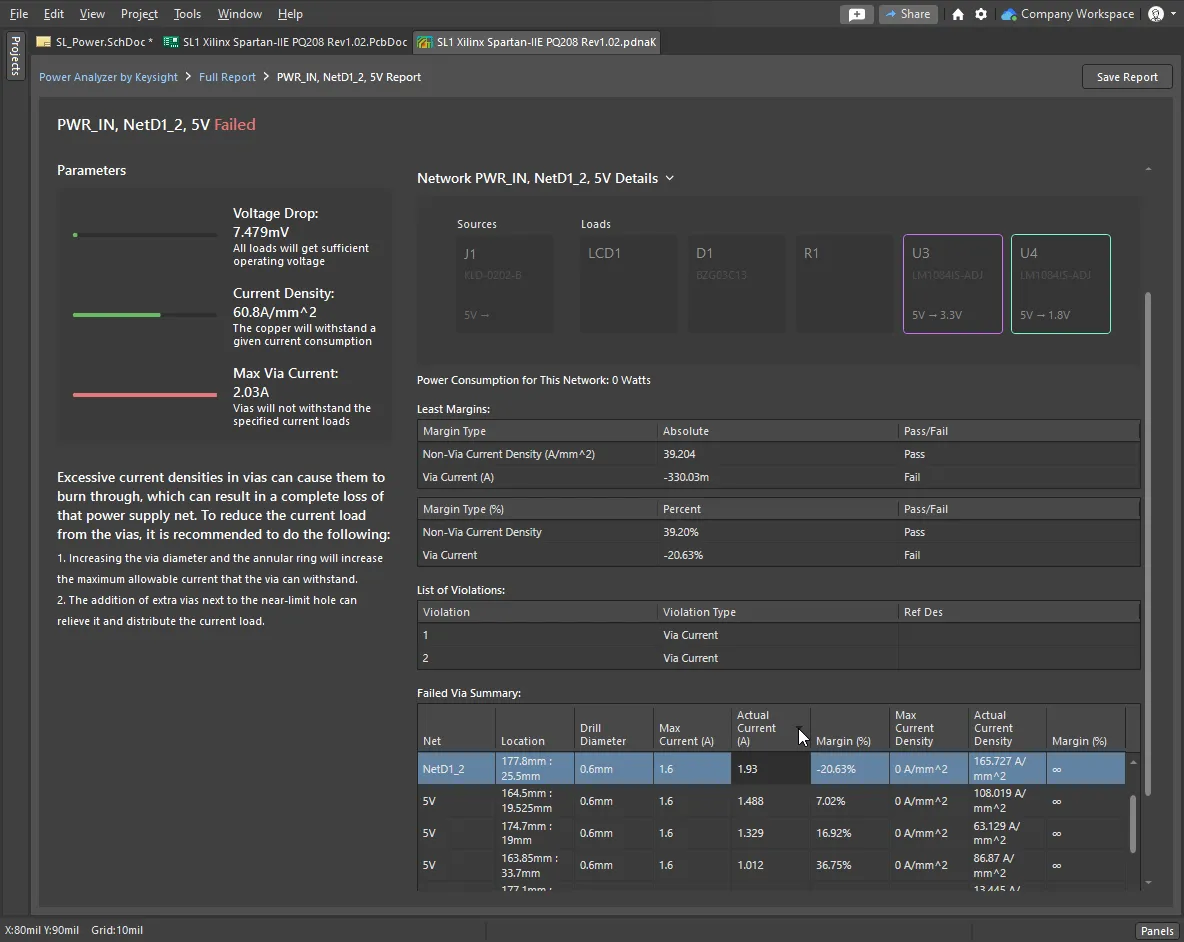
Интерпретация результатов и формирование отчёта
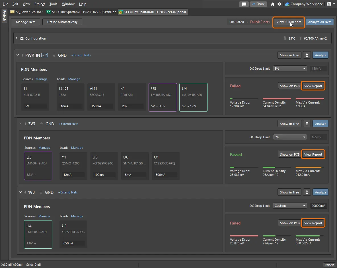
Power Analyzer предоставляет подробную обратную связь прямо в редакторе PCB. На панели Power Analyzer by Keysight можно быстро исследовать нарушения, расставлять измерительные зонды и сохранять тепловые карты в виде изображений. Чтобы получить подробную информацию о DC-анализе питания вашей платы, можно сформировать отчёт. Подробный отчёт открывается внутри документа pdnaK, и оттуда можно сохранить выбранные разделы в HTML-файл отчёта. Отчёт может быть сформирован как для отдельной силовой сети, так и для всей сети питания.
Работа с интерактивными графическими результатамиРаботая с интерактивной панелью Power Analyzer by Keysight, вы можете быстро находить и анализировать нарушения. Формирование отчётаЧтобы сформировать подробный отчёт, нажмите кнопку Подробный отчёт по сети — параметрыПолный отчёт (Full Report) перечисляет все силовые сети, которые были проанализированы; щёлкните по имени сети (Net Name), чтобы открыть подробный отчёт по этой сети. В левой части отчёта по сети перечислено:
Подробный отчёт по сети — результатыВ правой части отчёта есть сворачиваемые разделы для:
Подробный отчёт по сети — детали сетиИспользуйте раздел Network Details , чтобы быстро выявлять потенциальные проблемы в проекте. В этом разделе перечислено:
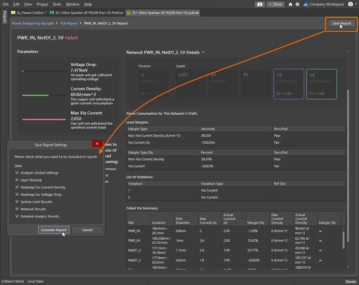
Сохранение отчётаЧтобы создать HTML-отчёт по анализам, нажмите кнопку
Включение результатов Probe и сохранённых изображенийИзображения, сохранённые с помощью кнопки |
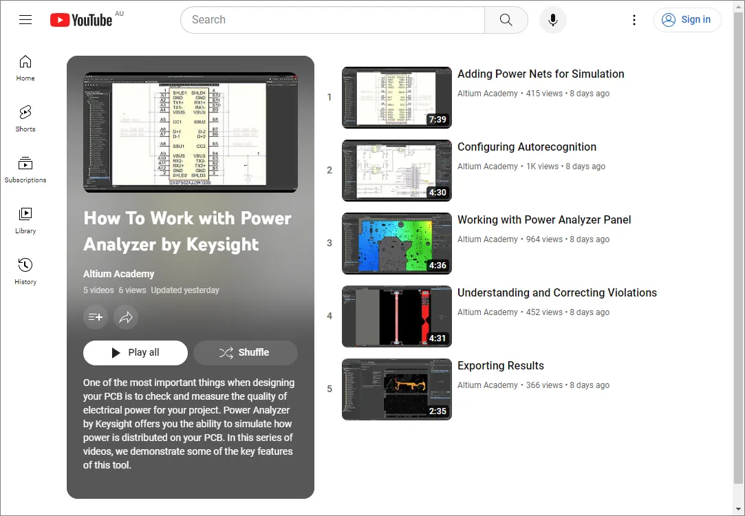
Плейлист — как работать с Power Analyzer by Keysight
Чтобы научиться работать с новым ПО для проектирования, требуется время. Если вам удобнее учиться по видео, посмотрите этот плейлист, в котором демонстрируются некоторые ключевые возможности: How to Work with Power Analyzer by Keysight.
 Локализовано с помощью ИИ