
Creating the Layout Drawing
Once the harness design has been captured in the form of a wiring diagram, the physical representation of the design can be created as a harness layout drawing (*.LdrDoc). Add this document to the harness project from the Projects panel by right-clicking on the project entry and then selecting Add New to Project » Harness Wiring Diagram from the context menu (or use the File » New » Harness Layout Drawing command from the main menus).
Setting Up a Harness Layout Drawing Document
Options of a layout drawing document can be configured in the Properties panel when no object is selected in the document's design space. The main settings are:
-
In the General region of the panel's General tab – select the measurement units that apply to the document and its graphic elements and set the grids to enable easier placement. Altium Designer offers three grid types: visible grid for navigation, snap grid for placement, and snap distance for aiding the creation of connections.
-
In the Page Options region of the panel's General tab – configure document sheet size and title block or select from available harness layout drawing templates.

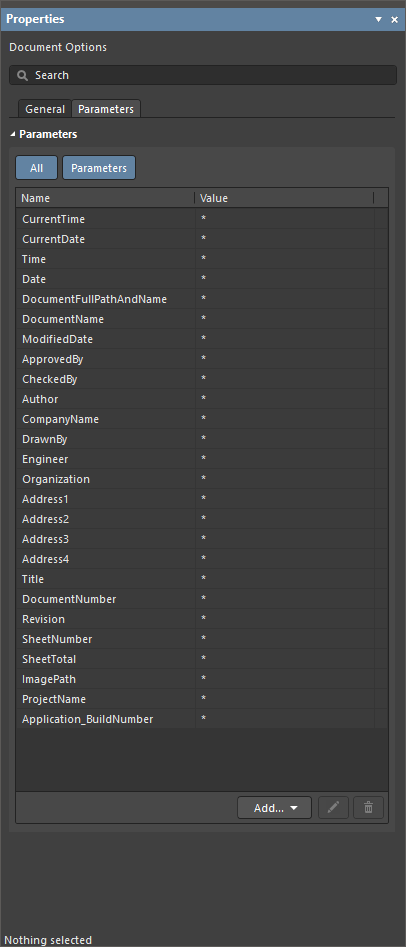
The General and Parameters tabs of the Properties panel when no object is selected in the harness layout drawing document
Importing Data from the Wiring Diagram
Select the Design » Import Wiring Diagram command from the main menus to import the design data from the wiring diagram. The component will be placed on the layout drawing sheet in the relative positions defined in the wiring diagram. Connection points associated with components will also be placed next to each component on the layout drawing.

A harness layout drawing document with the imported data from the wiring diagram
 ).
).Working with Components
Initially, each component is represented on the layout drawing with its symbol. Properties of a placed component can be configured in the Properties panel when the component is selected in the design space. The Properties panel for a component includes the following tabs:
-
General – general properties of the component, such as designator and comment, location, model representation, parameters, etc.
-
Pins – the list of component pins.
-
Cavities – a read-only view of socket cavities assigned to the component. Cavity assignments can only be modified in the wiring diagram – learn more.
-
Associated Parts – allows additional parts, such as heatshrink, to be assigned to the component.

Configuring Representation of a Component
Using the Graphical Symbol / Physical Model option in the Model region of the Properties panel (under the General tab) when a component is selected, you can toggle between the symbol representation (the component's symbol) and the 3D model projection (the component's footprint). Use other settings in the panel's region to configure the representation.
|
A component represented by its schematic symbol The same component represented by the projection of its 3D model |


When using the Physical Model representation, use the Style options to display the model either as a Solid (no lines) or as a Wireframe. Use the options of the Side drop-down to select the desired side of the model's view (orthogonal and isometric options are available). The below images demonstrate some of the settings with the corresponding results in the design space.


 ).
).Defining Physical Arrangement on a Harness Layout Drawing
All physical connections within the harness are defined as harness bundles (even if a bundle contains just a single wire). Each bundle must start and end at a connection point. At the initial import of harness design data (as described above), each component has a connection point automatically placed next to it, and this connection point is associated with the component and all of its pins. If required by the design's physical structure, new connection points can be placed, and assigned objects of a connection point can be configured.
 ).
).Working with Connection Points
To place a new connection point, use the Place » Connection Point command from the main menus. Connection points are displayed in the design space as shown below.

Properties of a placed connection point (its location, visual representation, etc.) can be configured in the Properties panel when the connection point is selected in the design space.

The Properties panel when a connection point is selected
 ).
). ).
).Assigning Objects to Connection Points
Objects assigned to a connection point can be configured as needed according to your design intent. One or multiple objects (components, splices/taps, 'no connect' objects, and shields with connection) can be assigned to a connection point using the Add Assigned Objects dialog accessed by clicking the ![]() button in the Assigned Objects region of the Properties panel.
button in the Assigned Objects region of the Properties panel.

 ).
).When a component is assigned to a connection point, a dash-dotted line is displayed in the design space between the component and the connection point, as shown below. In the Properties, you can select which component pins are assigned. Click the cell in the Pins column of the grid in the Assigned Objects region to access the drop-down to select the required component pins.

Working with Harness Bundles
To place a new harness bundle, use the Place » Harness Bundle command from the main menus (shortcut: Shift+B).
After selecting the command, click a connection point (a red cross appears at the cursor when it is over a connection point's hotspot) to place the start point of the harness bundle. Position the cursor and click to anchor a series of vertex points that define the shape of the harness bundle. After placing the final vertex point at another connection point's hotspot, right-click to complete placement.
By default, a harness bundle is placed using Any Angle placement mode. When placing a harness bundle, press Shift+Spacebar to cycle through placement modes. The mode specifies how corners are created when placing bundles and the angles at which bundles can be placed. While in the 90 Degree or 45 Degree mode (true orthogonal modes), press Spacebar to cycle between the start and end sub-modes. The current mode and sub-mode are shown in the Status Bar.

An example of a harness bundle placed between connection points CP1 and CP_P2.
When placed and selected, a harness bundle’s vertices can be dragged to change the angle between two adjacent sections.
Properties of a placed harness bundle (location, visual representation, etc.) can be configured in the Properties panel when the harness bundle is selected in the design space.

The Properties panel when a harness bundle is selected
Each harness bundle will automatically contain the objects (wires and/or cables) according to the connectivity defined in the wiring diagram. These objects are listed in the Bundle Objects region of the Properties panel when the bundle is selected. Click an object in this list to highlight all bundles the selected object passes through.

Using the Length field in the panel's Properties region, you can define the length of the selected bundle. Lengths of wires and cables that pass through bundles are calculated based on Length values of these bundles. Calculated values of wire/cable length are shown in the Length Value column of the grid in the panel's Bundle Objects region.
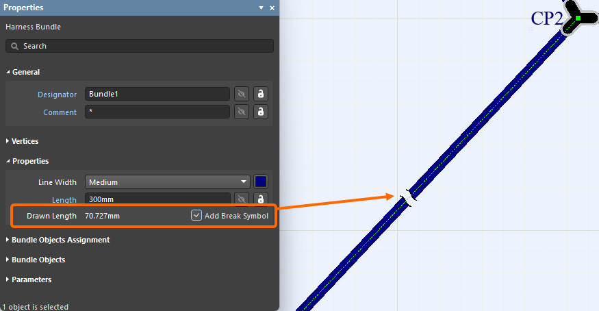
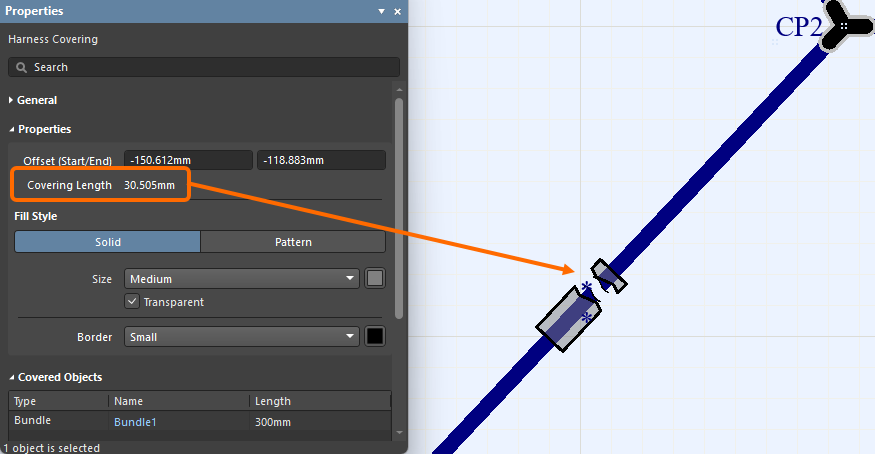
Adding a Break Point
A break point, which is used as an indication that the bundle is Not to Scale (NTS) can be placed on a harness bundle. The bundle will display a break symbol in the middle of its longest segment as shown in the first image below, and the properties will display the Drawn Length. To place a break, enable the Add Break Symbol option in the Properties region of the bundle properties. Harness coverings that cover a harness bundle with a break point will also display the break in the same location. If the harness covering ends at the harness bundle break point, the covering will be drawn slightly longer, as shown in the second image.
 ).
).Bundles with Wires from Split Cables
All harness bundles that include wires from a split harness cable are highlighted on the layout drawing when the cable is selected in the Bundle Objects region of the Properties panel. The length of a split cable is determined by the length of the longest wire.
|
Cable C1 is split between different connectors. When clicking the cable entry in the Bundle Objects region of the Properties panel for the selected bundle, all bundles that include wires from C1 are highlighted. The length of the cable is determined by the length of the longest wire (in this case, the wires that pass through bundles B1 and B3 are the longest). |


No Connect Objects Within a Cable
If the wiring diagram includes 'no connect' objects within a cable, there is no need to add these objects to connection points in the layout drawing. The harness bundle will correctly recognize objects of the cable. See an example in the images below.
|
A cable in the wiring diagram document contains unconnected wires (W4 and W5). The 'no connect' objects are not assigned to the connection points in the layout drawing. However, the bundle correctly recognizes all objects of the cable (including wires W4 and W5). |


Jumper Wires
Jumper wires can be displayed in the layout drawing. When the wiring diagram of a harness project includes a wire that connects cavities of the same harness connector, this wire is shown in the Properties panel as an object of the harness bundle that corresponds to the harness connector on the project's layout drawing when the harness bundle is selected in the design space.


Covering Harness Bundles
A harness covering object (Place » Harness Covering) can be placed over a harness bundle. The length of the covering can be graphically modified in the design space during or after placement.
After selecting a harness covering placement command, an orange dot will appear in the design space when the cursor is over a harness bundle, which signifies that the harness covering can be placed (a gray dot signifies that a harness covering cannot be placed at that specific place). Click where you want the covering to begin, then move the cursor along the bundle to the point you want the covering to end, then click again. Harness coverings can overlap one another, as demonstrated in the video below.
Properties of a placed harness covering can be configured in the Properties panel when the harness covering is selected in the design space.

The Properties panel when a harness covering is selected
You can define the size of a harness covering object relative to the size of the bundle it is covering (the bundle's Line Style) using the Size drop-down in the Properties panel. Scroll through the images below to see examples of different sized harness coverings with various harness bundle sizes.


Harness coverings can also be configured as patterned. In the Fill Style region of the Properties panel, select Pattern, then use the Pattern drop-down to choose the desired weave color (black, yellow, or red).


The start of a covering is taken as the left-most, top-most point of its path, and the path includes only the bundles the covering lays on.
You can apply/extend a harness covering over a junction point (a connection point in the layout drawing where two or more bundles come together). This removes the need to have separate harness coverings between junction points in a section that contains several connectors.

Adding Layout Labels
Physical labels can be placed into the layout drawing (Place » Layout Label).

Properties of a placed layout label (its designator, text, visual representation, etc.) can be configured in the Properties panel when the layout label is selected in the design space.

The Properties panel when a layout label is selected
When defining the label's text in the Text field, use Ctrl+Enter or Shift+Enter to add a new line of text. Enable Show only first line to display only the first line of the Text field in the design space. The layout label text can also be aligned according to your needs using the Alignment controls.


 )
) ).
). ).
).Updating Layout Drawing Objects from Libraries
The following objects can be updated from their source Workspace library:
-
Harness components
-
Parts associated with harness components
-
Parts associated with connection points
-
Harness coverings
-
Layout labels
When an object is selected, the information about the linked Workspace component can be found in the Properties panel (e.g., the Associated Parts tab for a harness component's associated parts or the General region for a layout label).
If there is a later revision of the Workspace component available, the entry for the revision status will reflect this using the text Out of date. At the individual object level, the link can be updated to the latest revision of the Workspace component by clicking the ![]() button.
button.

An example of indicating an out-of-date harness component revision
The Update from Libraries feature (Tools » Update from Libraries) can also be used to update out-of-date components linked to the objects listed above. Note that for an object be included into the update using the Update from Libraries feature, a component assigned to the object must include a link to a schematic symbol.

Annotating Harness Layout Drawing Objects
Use the commands in the Tools » Annotation menu to annotate the following objects in the harness layout drawing document:
-
Harness components
-
Connection points
-
Harness bundles
-
Harness coverings
-
Layout labels

Annotating objects in a harness layout drawing document is similar to annotating components in a schematic document (*.SchDoc) of a PCB design project. Use the following links to learn more about annotation commands available for a harness layout drawing document:
Cross Probing between Wiring Diagram and Layout Drawing
Cross-probing between the wiring diagram and layout drawing of a harness project is supported. The Cross Probe command can be accessed on the Tools main menu and the right-click menu in the design space.
Cross-probing can be performed:
-
Between components in the wiring diagram and layout drawing.
-
From a wire in the wiring diagram to the bundle(s) through which this wire passes in the layout drawing.
-
From a bundle in the layout drawing to the wire(s) that pass through this bundle in the wiring diagram.
|
Cross-probing from a component in the wiring diagram to the corresponding component in the layout drawing. Cross-probing from a component in the layout drawing to the corresponding component in the wiring diagram. Cross-probing from a wire in the wiring diagram to the corresponding bundles in the layout drawing. Cross-probing from a bundle in the layout drawing to the corresponding wires in the wiring diagram. |


