
xSignals での高速設計
課題
デバイスのスイッチング速度がますます高速化するにつれ、信号の完全性(シグナル・インテグリティ)を維持し、信号のタイミング要件を満たすことが課題になります。シグナル・インテグリティは、制御インピーダンス配線によって管理できます。これは、PCBスタックアップと、各層で使用する配線幅を慎重に設計することで実現します。
タイミング要件は、信号経路の配線長を一致させることで満たします。出力ピンから単一の入力ピンへそれぞれ接続される2ピンの信号経路の集合であれば、長さの算出と比較は単純です。しかし一般的な設計では、信号経路中に直列終端部品が入っていたり、信号に2ピンを超えるピンが含まれていたりすることが多く、その場合は下図に示すように、Balanced TやFly-Byの配線トポロジを用いて配線されることがあります。

Balanced Tトポロジで配線された4個のDDR2 RAMチップ。 ##
解決策
設計者の仕事は、タイミング・バジェットを満たすために許容される最大配線長といった設計要件を、タイミングを確実に満たすためのLengthルールや、潜在的なタイミング不一致を検出するMatched Lengthルールといった設計ルールのセットへ落とし込むことです。
設計者は信号を機能の観点で捉えます(例:「このアドレス信号はこのコネクタから各メモリデバイスへ配線する必要がある。そのため終端抵抗を末端に置いたfly-byトポロジで配線する。さらにソース側に直列終端が必要かもしれない」)。アドレスA0が終端抵抗を通過していても、設計者にとっては抵抗の反対側でもその信号は依然としてA0です。
しかしPCBエディタは、各信号を単に接続されたピンの集合(一般にネットと呼ばれる)として扱います。— ネットA0はこのコネクタのピンからこのメモリ部品のピンへ、次にこのメモリ部品のピンへ…という具合です。直列終端抵抗を追加した瞬間、そのアドレス線は2つの独立したネットになります。これにより、LengthやMatched Lengthといった重要な設計要件(設計ルール)を設計者が指定しにくくなります。
これは、xSignals (or extended Signal) という機能で管理できます。この機能により、高速信号経路を、終端部品や分岐を含めて、ソースとデスティネーション間を信号が伝搬する「経路」として正しく扱えるようになります。
新しいxSignalの作成
xSignalは、2つのノード間の設計者定義の信号経路です。 同一ネット内の2ノードの場合もあれば、異なるネット内の2ノードの場合もあります。
xSignalsは、次の方法で定義します。
- xSignals Multi-Chip Wizardを使用します。 これがxSignal作成の最も一般的なアプローチで、以下で説明します。
または、最初に対象オブジェクトを選択してから適切なコマンドを選ぶ、次の方法もあります。
-
選択したパッドに基づいて単一のxSignalを作成します。必要な開始パッドと終了パッドを選択します(直列終端部品がある場合、これらのパッドは異なるネットに属していても構いません)。パッドは設計空間で直接選択するか、PCBパネルをNetsモードで使用してパッドを検索・選択できます(下図参照)。パッドを選択したら、設計空間で選択したパッドを右クリックしてxSignals » Create xSignal from Selected Pinsコマンドを実行するか、PCBパネルで選択したパッドのいずれかを右クリックしてCreate xSignalコマンドを実行します。新しいxSignalは、PCBパネルのxSignalsモードに一覧表示されます。
- ソース部品を選択し、選択した部品を右クリックしてコンテキストメニューからxSignal » Create xSignals between Components コマンドを選択します。Create xSignals Between Componentsダイアログが開き、選択したソース部品が選択状態になります。このダイアログは以下で説明します。
- 設計空間で1つ以上の直列部品を選択し、選択した部品のいずれかを右クリックしてコンテキストメニューからxSignal » Create xSignals from Connected Nets コマンドを選択します。Create xSignals From Connected Netsダイアログが開きます。選択したソース部品と、その部品に接続されているネットが選択されます。このダイアログは以下で説明します。
- 既存のxSignal内にxSignalを作成したい場合もあります。その場合は、PCBパネルのxSignalモードを使用できます。パネル上部のSelectオプションが有効になっていることを確認し、現在のxSignalを見つけ、パネルのxSignal Primitivesセクションで必要なパッドを選択します。次に、設計空間で選択したパッドのいずれかを右クリックし、このリストの手順2で説明した方法を使って処理を完了します。

パネルのNetsモードで2つのパッドを選択し、選択したパッドのいずれかを右クリックしてCreate xSignalを選択します。パッドが異なるネットに属している点に注意してください。
xSignals Multi-Chip Wizard
xSignals Multi-Chip Wizardは、単一のソース部品と複数のターゲット部品の間にxSignalsを作成するために使用します。Wizard は、潜在的なxSignalsを特定するために部品指向のアプローチを採用しています。— 単一のソース部品、対象となるネット、ターゲット部品を選択すると、Wizard がソース部品から指定先部品までのすべての潜在的な経路を解析します。解析では、直列の受動部品を通過する経路や、あらゆる分岐に沿った経路も考慮されます。設計者は、生成したいxSignalsを選択でき、必要に応じてMatched Length設計ルールも作成できます。Wizard は、さまざまな一般的なインターフェース回路やメモリ回路に対して、xSignalsとxSignalクラスを自動作成するためにも使用できます。
このウィザードは複数回実行できるツールでもあります。— xSignal Routesページで最初に作成するxSignalsのマスターグループ全体から、そのサブセットを選択してクラスとルールを定義し、その後マスターグループに戻って別のサブセットを選び、クラスとルールを定義する…という作業を繰り返せます。
Wizard の大きな強みの1つは、Wizard とPCBエディタ間の連携が容易なことです。ウィザードのどのページでもxSignalをクリックすると、PCB上でパッドと配線(存在する場合)が視覚的にハイライト表示されます。
現時点では、ウィザードはTジャンクション識別子(tie-pointやbranch-pointとも呼ばれます)の自動追加をサポートしていません。設計に分岐配線が含まれる場合は、次を推奨します。
- (存在する場合)ソース部品から受動部品(直列終端抵抗など)までの長さを調整する。
- 各分岐について、Tジャンクションからデスティネーション部品までの長さを調整する。
- 必要に応じて、受動部品(受動部品がない場合はソース)からTジャンクションまでの残りの長さを調整する。
xSignals Multi-Chip Wizardにアクセスするには、メインメニューからDesign » xSignals » Run xSignals Wizardコマンドを選択するか、PCBレイアウト上で右クリックしてxSignals » Run xSignals Wizardを選択します。ウィザードの開始ページが表示されます。

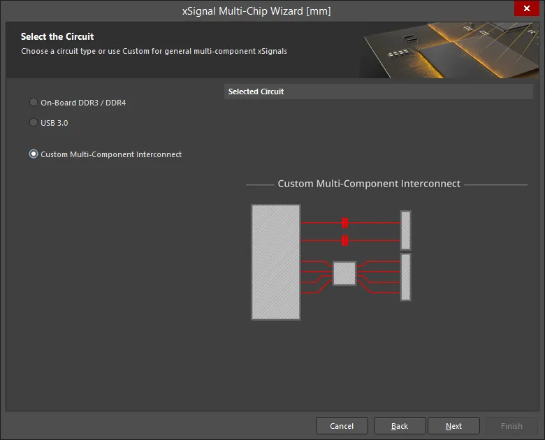
xSignals Multi-Chip Wizard
xSignals Multi-Chip Wizardの開始ページ
Wizardの2ページ目では、Custom Multi-Component Interconnect、On-Board DDR3 / DDR4、またはUSB 3.0のいずれかを選択するよう求められます。Custom Multi-Component Interconnectモードは、選択したソース部品と複数のターゲット部品の間に複数のxSignalsを定義するために使用します。一方、On-Board DDR3 / DDR4 モードはDDR3またはDDR4メモリ用のxSignalsを作成するために使用します。USB 3.0モードは、各USB 3.0チャネルに対してxSignals、xSignal Classes、Matched Lengthルールを作成します。用途に応じて適切なモードを選択してください。
The Custom Multi-Component Interconnect Mode
このモードでは、ウィザードを使用して、選択したソース・コンポーネントと複数のターゲット・コンポーネント間に複数のxSignalを定義できます。ウィザードは、潜在的なxSignalを特定するためにコンポーネント指向のアプローチを採用しています。単一のソース・コンポーネント、対象となるネット、宛先コンポーネントを選択すると、ソース・コンポーネントから宛先コンポーネントまでのすべての潜在的なパス(直列の受動部品を通過し、分岐も含む)を解析します。その後、設計者が生成したいxSignalを選択します。ウィザードでは、コンポーネント間の複数ネットに対するエンドツーエンドのxSignalを定義できるだけでなく、それらのエンドツーエンド信号の区間(ソース出力ピンから直列終端部品まで、直列終端部品から宛先入力ピンまで)に対するxSignalも作成できます。有効にした設定に基づき、ウィザードはxSignalクラスおよび Matched Net Lengths デザインルール(それらのxSignalを対象)も作成できます。ウィザードが完了したら、長さ調整(Length Tuning)プロセスを開始できます。
ウィザードは複数のページで構成されます。ページ数は回路構成によって異なります。たとえば直列終端がある場合は、追加ページが表示されます。各ページの設定内容を以下に示します。
ソース・コンポーネントの選択
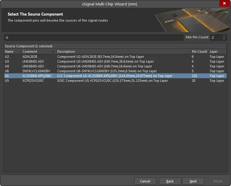
このページでは単一のソース・コンポーネントを選択します。グリッド上部の Filter および Min Pin Count フィールドを使用して、目的のコンポーネントを見つけやすくできます。ワイルドカード * と ? が使用できます。
ソース・ネットの選択
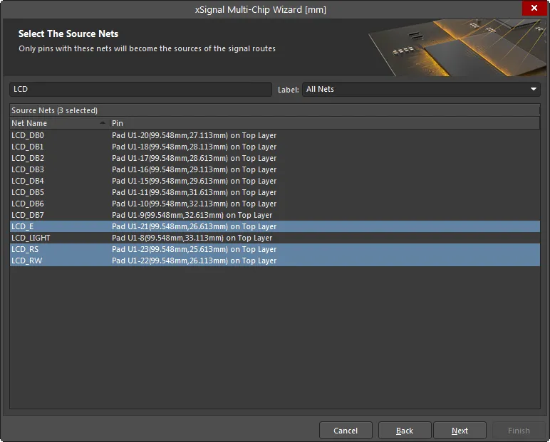
選択したソース・コンポーネントに接続されている、対象のネットを選択します。グリッド上部の Filter および Label フィールドを使用して 目的のネットを見つけやすくできます。リストされたネットを持つピンのみが、信号ルートのソースになります。
宛先コンポーネントの選択
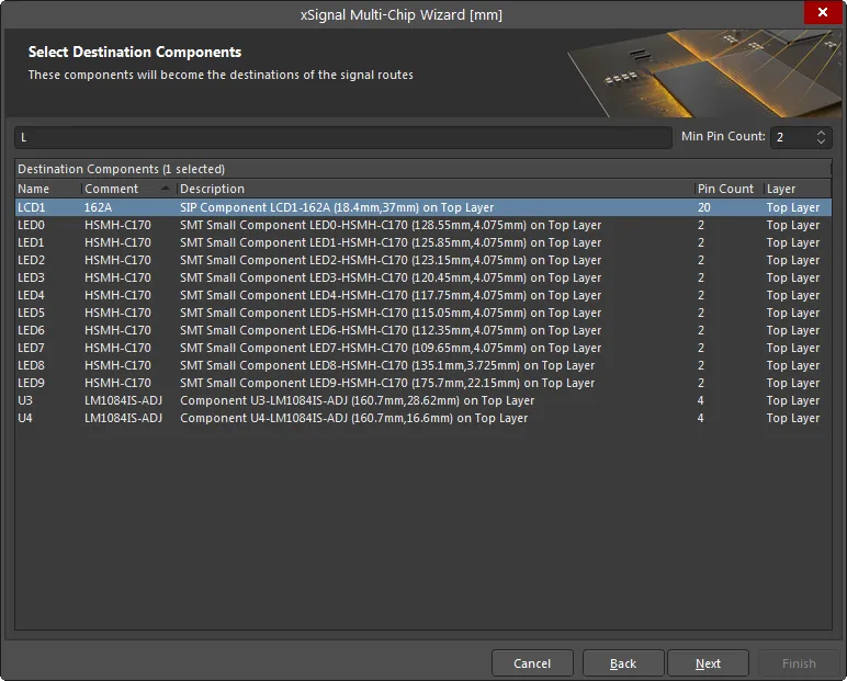
目的の宛先コンポーネントを選択します。グリッド上部のコンポーネント Filter および Min Pin Count フィールドを使用して 目的のコンポーネントを見つけやすくできます。
xSignalルート
このウィザードページには、各 Source Pin から各 Destination Pin までの提案xSignalが一覧表示されます。エントリをクリックすると、PCB上でそのxSignalがハイライト表示されます。
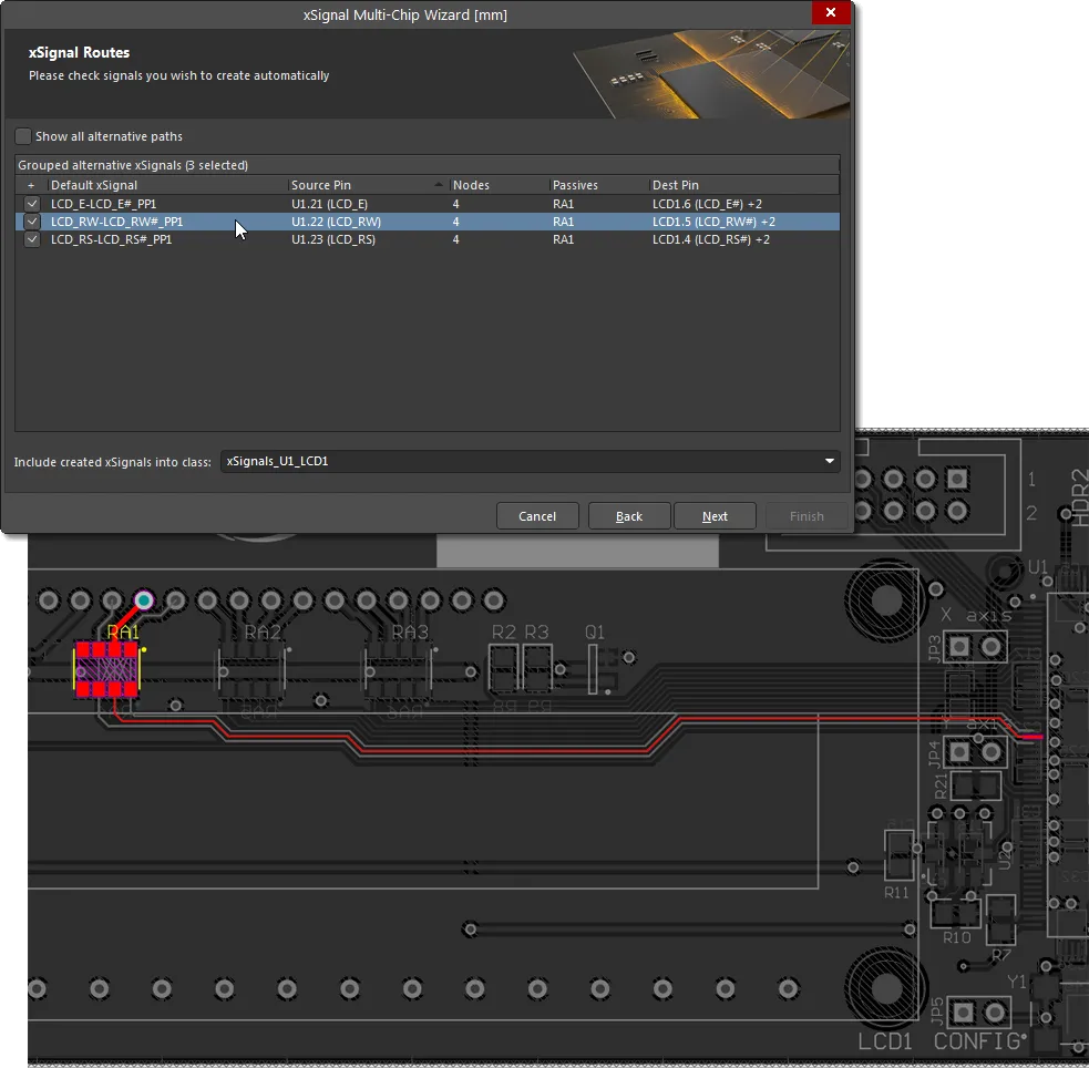
ネットパスを解析して潜在的なxSignalを特定した後、ウィザードは、関心のある組み合わせのみがリストされるようにセットを絞り込もうとします。これらはエンドツーエンドのxSignalです。上の画像は、ウィザードの前ページで選択したソース・コンポーネントと宛先コンポーネント間のものを示しています。また、各ルートで直列終端部品RA1が検出されたことも示しています。RA1は実際には4連の抵抗パックです。この状況では、ウィザードは自動的に論理的な関連付けを作成します。各抵抗がパックを横断して接続されていると仮定し、コンポーネント上で互いに向かい合うピンに接続されるネットをペアリングします。
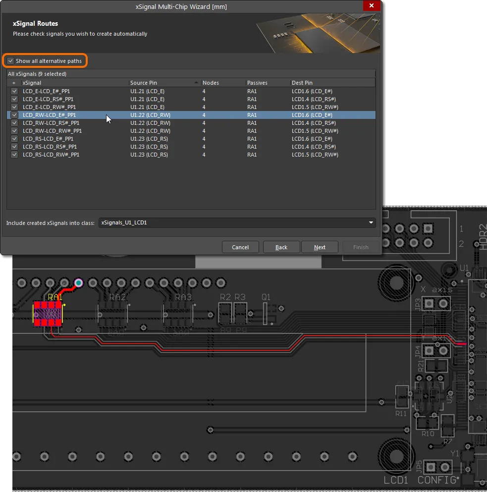
ただし、「各抵抗のピンが互いに向かい合っている」という仮定が常に正しいとは限らないため、Dest Pin 列のドロップダウンを使用して、他の利用可能な出力ネットを選択できます。あるいは、グリッド上部の Show all alternative paths オプションを有効にして、xSignal生成に使用できるネットの潜在的な組み合わせをすべて表示します。xSignalを作成したい行ごとにチェックボックスを有効にしてください。有効化されたxSignalは、このページ下部の Include created xSignals into class フィールドに表示されるクラスに追加されます。新しい名前を入力するか、ドロップダウンから選択します。
xSignals 長さ調整
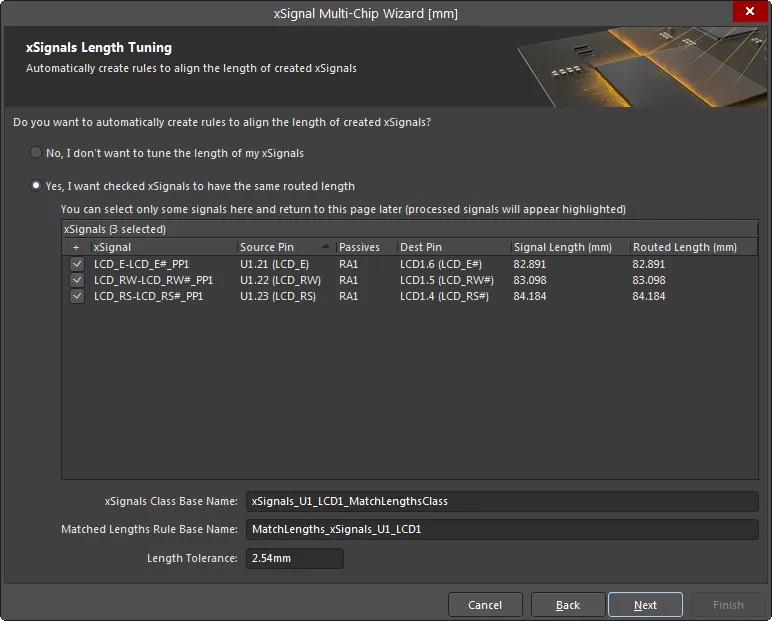
このページは、有効化されたxSignalに対して Matched Length デザインルールを自動作成するために使用します。この新しいデザインルールの対象にしたいxSignalを only 有効にしてください。設計上、要件の異なる複数のルールが必要な場合は、後続の工程で、まだルールが定義されていないxSignalに対して追加ルールを定義する機会が与えられます。この最初の段階では、全体のエンドツーエンドxSignalも提示されます。後続のウィザードページでは、xSignal内の区間(例:出力ピンから直列終端抵抗までの区間)に対するデザインルールを定義できます。
xSignalの長さを調整したくない場合は、No, I don't want to tune the length of my xSignals を有効にしてください。このオプションが有効な場合、このページの他のオプションは使用できません。他のオプションを編集・利用できるようにするには、Yes, I want checked xSignals to have the same routed length を有効にしてください。
xSignals Class Base Name フィールドは、現在選択されているxSignalの名前を定義するために使用します。他のxSignalに対してこの処理を繰り返す可能性があることを念頭に、意味のある名前を入力してください。このxSignalセットは、Matched Lengths Rule Base Name フィールドに入力した名前のデザインルールによって、指定した Length Tolerance でターゲット化されます。
ソース→受動部品 長さ調整
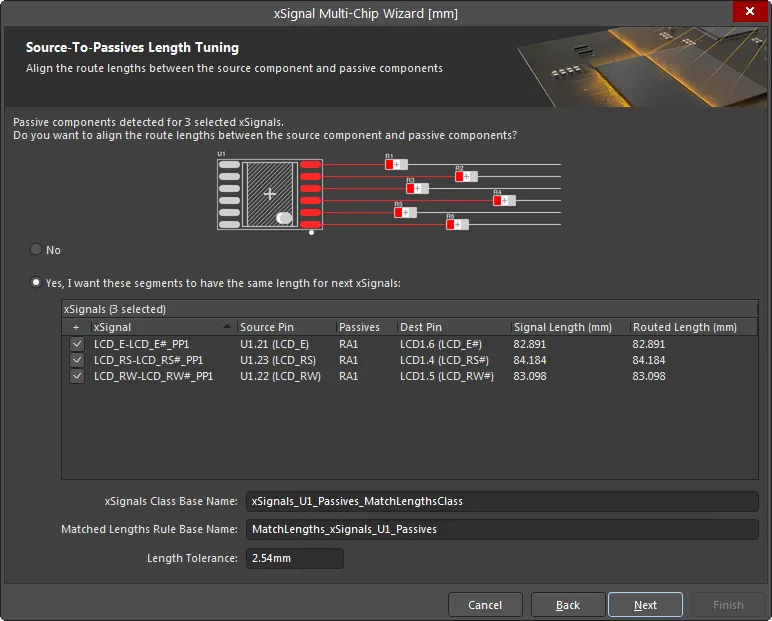
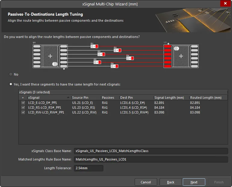
選択したネットのセットに直列終端部品が含まれている場合、追加のウィザードページが表示され、これらのネット区間に対して追加のxSignalおよびデザインルールを作成できます。上の画像では、このウィザードページを使用して、ソース・ピンから終端部品まで走る選択xSignalに対する Matched Length デザインルールを作成しています。これらに対してxSignal/xSignalクラス/デザインルールが必要な場合は、Yes, I want these segments to have the same length for next xSignals オプションを有効にし、必要なxSignalを有効化して、xSignals Class Base Name、Matched Lengths Rule Base Name、Length Tolerance を定義してください。この Matched Length ルールで使用するための追加xSignalが作成されます。
受動部品→宛先 長さ調整
このページは、終端部品から宛先ピンまで走る選択xSignalに対する Matched Length デザインルールを作成するために使用します。必要な場合は Yes, I want these segments to have the same length for next xSignals オプションを有効にし、必要なxSignalを有効化して、 xSignals Class Base Name、Matched Lengths Rule Base Name、Length Tolerance を定義してください。この Matched Length ルールで使用するための追加xSignalが作成されます。
レポートと続行
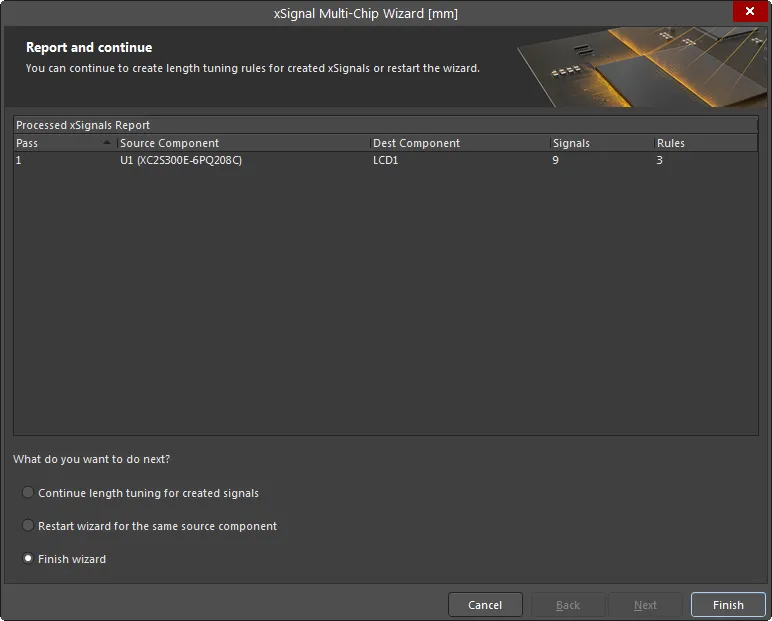
このウィザードページでは、作成される予定のxSignal数と、作成される予定のデザインルール数が詳細表示されます。
ページ下部では次を選択できます。
- Continue length tuning for created signals – 前ページで特定のxSignalを無効にしており、いまそれらのxSignalに対して追加ルール定義のプロセスを進める必要がある場合に選択します。
- Restart wizard for the same source component – これらの設定を破棄し、同じコンポーネント/ネット選択のままウィザードを再開始したい場合に選択します。
- Finish wizard – このソース・コンポーネントに対するxSignalおよびデザインルール作成が完了した場合に選択します。
これらのxSignalは長さ調整の準備ができています。開始するには、メイン Route メニューまたは Active Bar から Interactive Length Tuning オプション( )を選択します。
On-Board DDR3 / DDR4
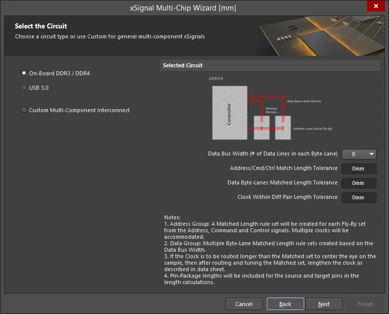
このモードでは、オンボードDDR3/DDR4向けに、ウィザードがxSignal、xSignalクラス、Matched Lengthグループ、Diff Pair Matched Lengthsルール、およびFly-Byトポロジを自動的に作成します。ウィザードは、フライバイ配線トポロジが使用されることを前提としています。
ソース・コンポーネントの選択
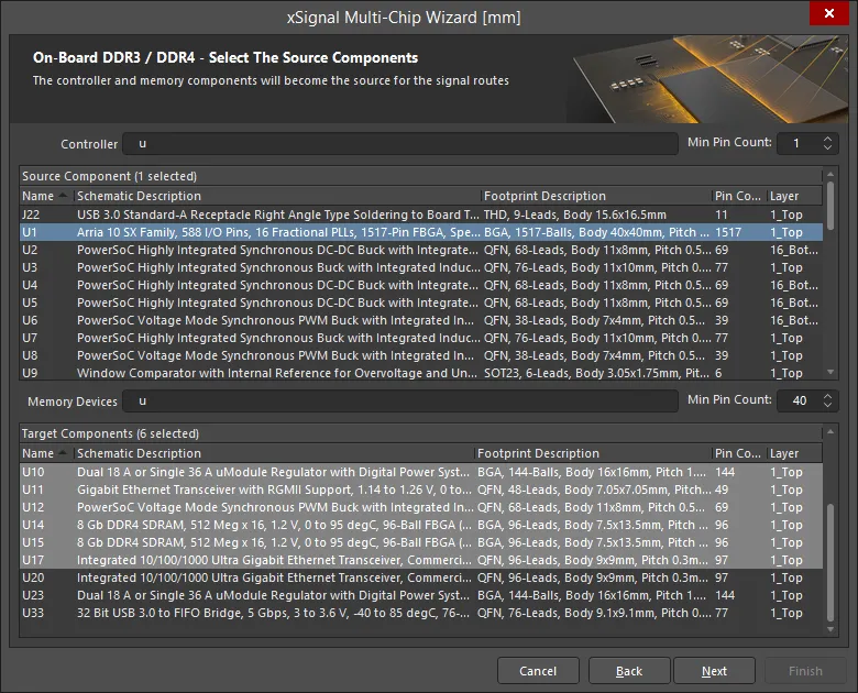
このページでは、Wizard が、デジグネータのプレフィックスとピン数に基づいて、潜在的なソース・コンポーネントおよびターゲット・コンポーネントをすべて識別します。Controller/Memory Devices フィールドを使用してコンポーネント/メモリデバイスをフィルタし、上下矢印で Min Pin Count を必要に応じて設定します(Source Component と Target Components の両方に対して)。その後、単一のソース・コンポーネントを選択し、ターゲット・コンポーネントを選択します。
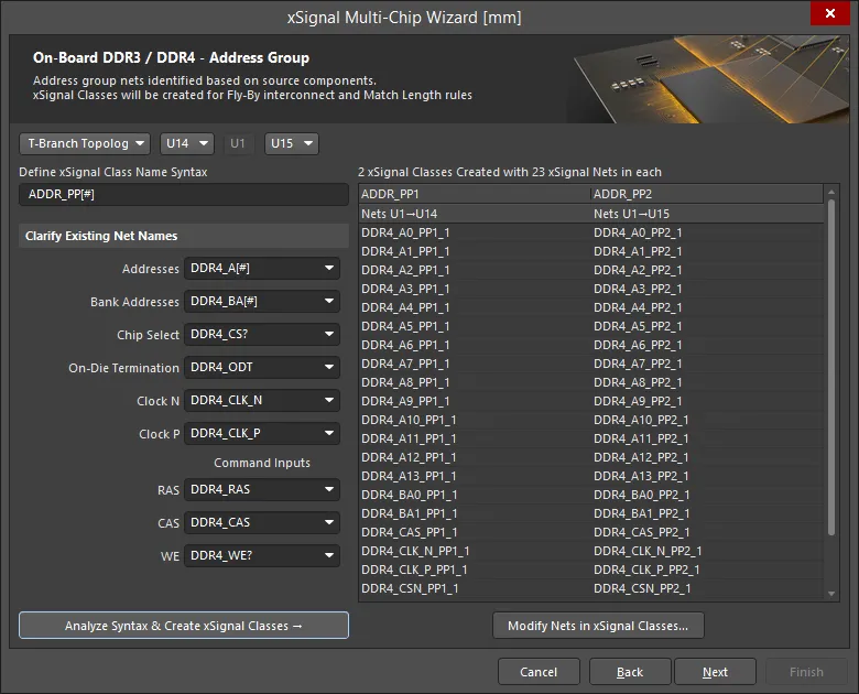
アドレス・グループ
このページの機能は次のとおりです。
- Fly-By TopologyT-Branch Topology および T-Branch Topology オプションがサポートされています。ドロップダウンリストから必要なトポロジを選択します。
- Fly-By Topology を選択した場合、ターゲット・デバイスはフライバイ配線のポイント・ツー・ポイント順にリストされます。ソフトウェアは順序を自動的に決定しようとします。コンポーネント配置前にウィザードを実行した場合は、ドロップダウンコントロールを使用してポイント・ツー・ポイント順を手動で設定する必要があります。
- T-Branch Topology を選択した場合(上図のとおり)、ターゲット・デバイスの半分がソースの前に、残り半分が後に表示されます。必要に応じてドロップダウンコントロールでターゲット・コンポーネントの順序を設定してください。
- Define xSignal Class Name Syntax:
- 開始時のデフォルトは
ADDR_PP[#] - です。
[#]はメモリデバイス数を表します。 PPサフィックスは必要に応じて変更できます。
- 開始時のデフォルトは
- ウィザードはコンポーネントを解析し、設計内でこれらのサフィックスを探して、以下に詳述するアプローチで完全な名前構文を表示します。正しくない場合は更新してください。
- ここでの目的は、これらの機能に対応するネットを自動的に見つけることです。ネットが見つかったら、命名構文を各フィールドに入力します。
- その後、コンポーネント間のネットを確認し、サフィックスが見つかったらプレフィックスを特定します。たとえば、ウィザードはアドレス線を特定するために
_A[#]を探します。 - 「_」で始まるサフィックスを持つネットが見つからない場合は、「_」の後ろのテキストのみを探します。「-」や「.」などの代替セパレータもチェックします。
- 構文を自動判定できない場合は、これらのフィールドを手動で定義する必要があります。ドロップダウンを使用して、基板上の既存ネットから選択してください。
- 順序と命名構文を定義したら、Analyze Syntax & Create xSignal Classes ボタンをクリックして xSignals のリストを作成します。ウィザードは構文とコンポーネントの接続状況を確認し、ダイアログ右側のグリッドに表示される xSignal クラスを生成します。Classes Created の数はメモリデバイスの数と一致します。
- 作成されたクラス数(例:4)と、各クラス内の xSignal ネット数(例:26)。
- xSignals は、各 xSignal クラスごとに列にまとめられます。各クラスに対して Matched Lengths のデザインルールが作成されます。表のサブ見出しは、これらの xSignals のソースおよびターゲットコンポーネントを表します。
- 自動生成されたリストが不完全または不正確な場合は、Modify Nets in xSignal Classes ボタンをクリックして Edit xSignal Class ダイアログを開き、クラスに対してネットを手動で追加/削除します。なお、その後に Analyze Syntax & Create xSignal Classes ボタンを再度クリックすると、手動変更は失われます。
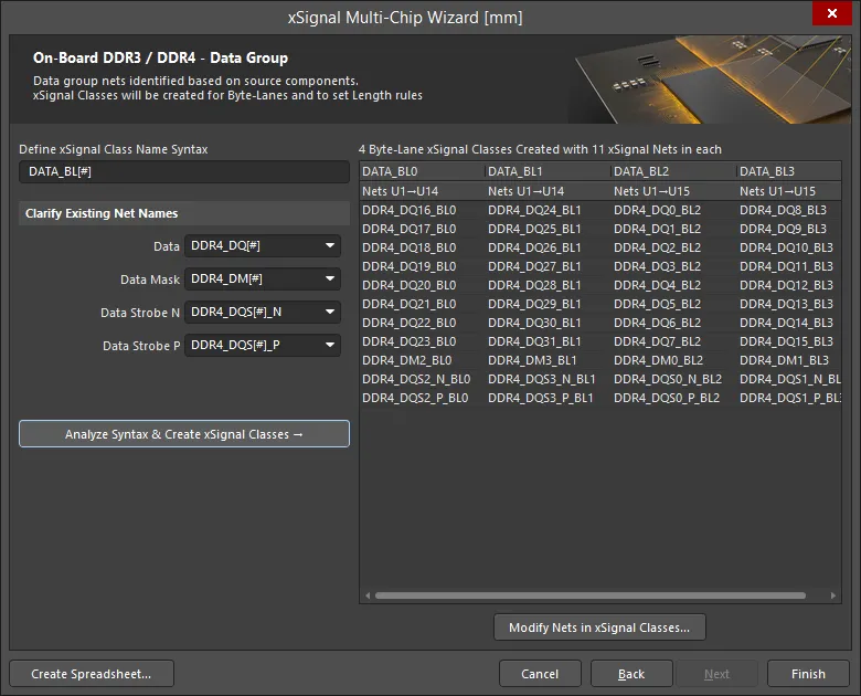
データグループ・ネットの特定
最終段階では、データグループに属するすべてのネットを特定します。
このページの機能は次のとおりです。
- ユーザー定義の xSignal クラス名の命名構文:
- 開始時のデフォルトは
DATA_BL[#] - です。
[#]はバイトレーン数を表し、これは(データ線の総数)÷(先に定義したデータバス幅)で決まります。 BLサフィックスは必要に応じて変更できます。ウィザードはコンポーネントを解析し、設計内でこれらのサフィックスを探して完全な命名構文を表示します。正しくない場合はドロップダウンで更新してください。
- 開始時のデフォルトは
- 命名構文を定義したら、Analyze Syntax & Create xSignal Classes ボタンをクリックして xSignals のリストを作成します。ウィザードは構文とコンポーネントの接続状況を確認し、ダイアログ右側の表に表示される xSignal クラスを生成します。作成されるクラス数は、メモリデバイスに接続されているバイトレーン数と一致します。表エリアの上には、作成されたクラス数(例:8)と、各クラス内の xSignal ネット数(例:11)が表示されます。
- これらの xSignal クラスに対して Matched Lengths のデザインルールが作成されます。表のサブ見出しは、バイトレーン xSignals のソースおよびターゲットコンポーネントを表します。
- 自動生成されたリストが不完全または不正確な場合は、Modify Nets in xSignal Classes ボタンをクリックして Edit xSignal Class ダイアログを開き、クラスに対してネットを手動で追加/削除します。なお、その後に Analyze Syntax & Create xSignal Classes ボタンを再度クリックすると、手動変更は失われます。
- Create Spreadsheet ボタンをクリックすると、ウィザードが作成した xSignals の XLS 形式スプレッドシートを生成します。
- xSignals と xSignal クラスの作成
ウィザードは次の項目について xSignals と xSignal クラスを自動作成します。
Address Group ページで詳細が示されているアドレス xSignals。
- Data Group ページで詳細が示されているデータ xSignals。
USB 3.0
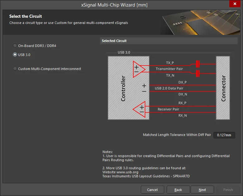
ウィザードは、ユーザーが指定した各コントローラ~コネクタのペア間にあるすべての USB 3.0 チャネルを処理できます。ウィザードはコントローラに接続された差動ペア・ネットを自動評価し、コネクタまで到達しているものを検出します。このスパンには受動部品や複数のネットが含まれる場合があります。ウィザードはこれらの各ペアを xSignal クラスとして識別し、ペアの各レッグはコントローラ~コネクタの xSignal として識別されます。
USB 3.0 を選択すると、このページには Matched Length Tolerance Within Diff Pair の設定が表示されます。適切な値を入力してください。この値はウィザードが作成するデザインルールで使用され、PCB Rules and Constraints Editor でいつでも変更できます。このようなユーザー定義設定は将来の使用のために保存されます。
USB 3.0 では、各 USB ユーザーポートは channel と呼ばれます。画像に示すように、各チャネルには Transmit、Receive、Data の 3 つの差動ペアが含まれます。
このページでは、ウィザードがデジグネータのプレフィックスとピン数に基づいて、候補となるソースコンポーネントとターゲットコネクタをすべて特定します。
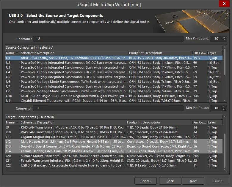
Controller のデジグネータ、Connector のデジグネータ、および Min Pin Count の値について、必要に応じてフィルタ用プレフィックスを設定します。
- ソースコンポーネントを 1 つ選択します。
- ターゲットコンポーネントを選択します。
- 複数のターゲットコンポーネントを選択した場合は、ウィザードの次ページにあるドロップダウンを使用して、各コンポーネントの xSignal およびネット命名構文を確認してください。
このページでは、ウィザードが該当する Transmitter、Receiver、Data のペア・ネットを識別し、それらを xSignals に含めるために使用する命名構文を定義します。各 xSignal のペアは xSignal クラスにクラスタリングされ、これらのクラスが Matched Length デザインルールのスコープとして使用されます。
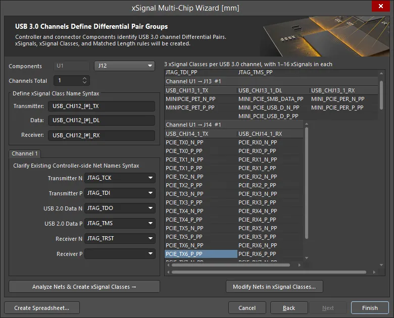
このページの機能は次のとおりです。
コントローラのデジグネータは Components ラベルの横に表示されます。その隣のドロップダウンには、ウィザードの前ページで選択したすべての Connectors が含まれます。
- 表示される命名構文オプションは、ドロップダウンに列挙された各コネクタに適用されます。各コネクタを順に選択し、選択した命名構文が完全で適切であることを確認してください。
- 前述のとおり、USB 3.0 では各 USB ユーザーポートは channel と呼ばれます。チャネル数(Channels Total)は 1~32 の範囲で設定できます。通常、各コネクタは 1 つのチャネルを持ちます。
各 USB 3.0 チャネルには、コントローラからコネクタへ伸びる Transmit、Receive、Data の 3 つの差動ペア経路があります。ウィザードは、必要に応じて直列部品をまたぐ形で、正側ネットごとに xSignal を 1 つ、負側ネットごとに別の xSignal を 1 つ作成し、さらにそのコントローラ~コネクタのペアを表す xSignal クラスを作成します。Define xSignal Class Name Syntax グループは、これらの xSignal クラス名を指定するために使用されます。ウィザードは、まだ定義されていない場合、適切な差動ペアも作成します。 - Define xSignal Class Name Syntax – 作成される xSignal クラスは指定どおりの名前になり、各チャネルには
[#]の代わりに数値が割り当てられます。必要に応じて任意の文字列を入力してください。– これらのフィールドは、該当する Transmitter / Receiver / Data のネット名を識別するために使用されるマスクを定義します。
- Define xSignal Class Name Syntax – 作成される xSignal クラスは指定どおりの名前になり、各チャネルには
- Channel <N>ウィザードには事前定義された命名スキームの大規模なテンプレートがあり、通常はこれらのフィールドを自動入力します。自動入力されない場合は、ドロップダウンから正しい名前を選択するか、適切なネット名の構文を入力してください。
- 命名フィールドを設定したら、Analyze Nets & Create xSignal Classes ボタンをクリックします。
- ウィザードは、すべてのチャネルについて xSignals、xSignal クラス、Matched Length ルールを作成します。これらはウィザードを再実行するたびに作成される点に注意してください。再度ウィザードを実行する予定がある場合は、事前に削除してください。
- 結果として得られた xSignal クラス名と、そのメンバー xSignals はグリッドに表示されます。
- Create Spreadsheet ボタンをクリックすると、ウィザードが作成した xSignals の XLS 形式スプレッドシートを生成します。
- Finish をクリックしてウィザードを完了します。
コンポーネント間の xSignals 作成ダイアログ
定義する xSignals の数が多い場合は、Create xSignals Between Components ダイアログを使用する方が効率的です。Design » xSignals » Create xSignals コマンドからアクセスできるこのダイアログでは、ソースおよび宛先コンポーネントが提示され、1 回の操作で 1 つまたは複数の xSignals を作成できます。

手順は次のとおりです。
Source Component を 1 つ選択します。
- 必要な Destination Components を 1 つ以上選択します。
- 対象の Source Net(s) を選択します。選択したソースコンポーネントに現在接続されているすべてのネットが一覧表示されます。特定のクラスに関連付けられたネットの場合は、Net Class ドロップダウンからそのクラスを選択します。
- Analyze ボタンをクリックします。ソフトウェアは、選択したネットについて、選択したソースと宛先コンポーネント間に存在する可能性のある xSignals を特定しようとします。選択したネットを含み、選択したソースと宛先コンポーネント間を走る可能性のあるすべての xSignals が xSignals フィールドに一覧表示されます。なお、解析アルゴリズムは選択したネットの現在のトポロジに従って処理するため、これが提案される xSignals に影響します。
- 解析が実行されると、ダイアログ下部に候補の xSignals が一覧表示され、すべて作成可能(有効)な状態になります。提案された xSignals のリストを注意深く確認し、必要なものだけを有効にしてください。右クリックのコンテキストメニューにあるコマンドを使用して、複数エントリをまとめて切り替えることができます。
- ダイアログ下部で必要な class を選択するか、名前を入力して新しいクラスを作成します。クラスを選択しなくても xSignals は作成され、Object Class Explorer ダイアログ(Design » Classes)で任意の xSignal クラスに追加できます。クラスを使用すると、デザインルールの作成と設定を大幅に簡素化できます。
- OK をクリックして xSignals を作成します。
ダイアログが閉じ、デザインスペースに戻ります。新しい xSignals は PCB パネルの xSignals モードに一覧表示されます。
接続ネットから xSignals を作成(Create xSignals From Connected Nets)ダイアログ
直列終端部品を含む xSignals を作成する場合は、Create xSignals from connected nets コマンドを使用するのが有効です。このコマンドは、コンポーネントを選択しているときに、メインメニューの Design » xSignals サブメニュー、または右クリックの xSignals サブメニューから利用できます。
このコマンドは、抵抗やコンデンサなどの選択した直列終端部品から外側へ向かって xSignals を構築するように設計されています。1 個以上のディスクリート部品、および抵抗ネットワークのような 1 個以上のマルチインスタンスのパック型部品の両方をサポートします。このコマンドを実行すると、 Create xSignals From Connected Nets ダイアログが開きます。

このダイアログを使用して、選択した直列部品をまたぐ xSignals を作成します。この例では 2 つの候補 xSignals が提案されていますが、作成されるのは 1 つだけです。
手順は次のとおりです。
- 単一の Source Component を選択します。
- 対象の Source Net(s) を選択します。選択したソースコンポーネントに現在接続されているすべてのネットが一覧表示されます。特定のクラスに関連付けられたネットの場合は、Net Class ドロップダウンからそのクラスを選択します。
- Analyze ボタンをクリックします。ソフトウェアは、選択したソースコンポーネントおよび選択したネットに対して存在し得る xSignals を特定しようとします。可能な xSignals はすべて xSignals フィールドに一覧表示されます。
- 解析が実行されると、ダイアログ下部に候補の xSignals が一覧表示され、すべて作成可能(有効)な状態になります。提案された xSignals のリストを注意深く確認し、必要なものだけを有効にしてください。右クリックのコンテキストメニューにあるコマンドを使用して、複数エントリをまとめて切り替えることができます。
- ダイアログ下部で必要な class を選択するか、名前を入力して新しいクラスを作成します。クラスを選択しなくても xSignals は作成され、Object Class Explorer ダイアログ(Design » Classes)で任意の xSignal クラスに追加できます。クラスを使用すると、デザインルールの作成と設定を大幅に簡素化できます。
- OK をクリックして xSignals を作成します。
ダイアログが閉じ、デザインスペースに戻ります。新しい xSignals は PCB パネルの xSignals モードに一覧表示されます。
ネット・トポロジの役割
xSignal を定義するとき、それは 2 つのノード(またはパッド)間で定義されます。しかし、PCB パネルの xSignals モードでその xSignal を選択すると、実際には 2 つのパッド間を結ぶ接続ラインの経路に沿って表示されます。これは、ソフトウェアがその xSignal が配線されると想定している経路であることを示しています。こうした動作になる理由は、そのネットに定義されたトポロジに従っているためです。ネット・トポロジは適用される Routing Topology デザインルールによって定義され、デフォルトのトポロジは Shortest です。
簡単なアニメーションでは、CPU が 4 個の DDR3 メモリチップに接続され、フライバイ配線戦略で配線される例を示しています。DRAM_A2 xSignal クラスには 4 つの xSignals が含まれています。まずクラスを選択し、次に各 xSignal を順に選択します。xSignal の経路がネットのトポロジに従っている様子が分かります。現在はデフォルトの Shortest に設定されています。

ネット・トポロジが Shortest に設定されているため、xSignals はプロセッサからメモリチップへ向かう必要な経路に従っていません。
xSignal 作成コマンド
Design » xSignals » Create xSignals コマンド以外にも、条件が満たされると xSignals サブメニューに他の xSignal 作成コマンドが表示されます。
以下に、コマンドと利用可能になる条件の概要を示します。
| コマンド | 説明 |
|---|---|
| Create xSignal from selected pins |
即座に作成単一の xSignal を即座に作成します。このコマンドは、デザインスペースで 2 つ以上のパッドが選択されている場合に利用でき、選択したパッドの 1 つを右クリックしたときに表示されるコマンドと同じです。 |
| Create xSignals between components |
このコマンドは、デザインスペースでコンポーネントが選択されている場合に利用できます。実行すると Create xSignals Between Components ダイアログが開き、コンポーネントが事前選択された状態になります。正しい Source と Designation コンポーネントが選択されていることを確認し、解析/作成プロセスを完了してください。 コマンドを起動すると、Create xSignals Between Components dialog が開きます。ダイアログを使用して次のように xSignals を作成します。
|
| Create xSignals from connected nets |
デフォルトでは、ソースコンポーネントのパッドに関連付けられたすべてのネットが(Source Component Nets 領域で)選択されます。必要に応じてこの選択を調整してください。
|
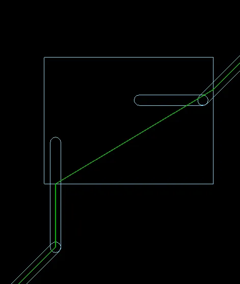
バランスTパターンにおける分岐点の定義
バランスT配線戦略の課題の1つは、Tポイント以降の幹線(トランク)と枝線(ブランチ)の長さをどのように等しくするかです。ネット内で利用可能なノードはパッド上にしかないため、トランク用、および分岐点から各枝の終端まで用に別々のxSignalを定義することはできません。分岐点は、下の画像の赤い点で示されています。
この問題を解決する方法の1つは、単一ピンのコンポーネントをネットに追加することです。設計で使用しているビアと同じサイズの単一パッドを持つコンポーネントを作成します。分岐点コンポーネントのパッドが単層であれば、ブラインド/ベリードビアと組み合わせて使用することもでき、ビアの開始層または終了層に配置することで、配線の作り方に対して完全な柔軟性が得られます。分岐点コンポーネントをPCBにのみ含めたい場合は、分岐点コンポーネントのTypeをMechanicalに設定してBOMから除外し、回路図との同期問題を防いでください。分岐点コンポーネントを回路図に含める予定がある場合は、コンポーネントのTypeをStandard (no BOM)に設定できます。

バランスT配線では、中間の分岐点間で長さを一致させる必要がある場合があります。
分岐点はネット内のノードであるため、これでトランクのみ、各主要ブランチ、必要に応じて各小ブランチについてもxSignalを定義できるようになります。これらを使ってマッチド長のデザインルールの適用範囲(スコープ)を設定でき、長さ合わせをどの粒度で行うかを設計者が完全に制御できます。
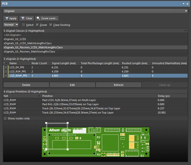
xSignalの管理
PCBパネルのモードでは、3つの主要領域が、現在のPCB設計のxSignal階層を反映するように(上から順に)変化します。
- xSignal Classes
- クラス
- 内の個々のxSignals
xSignalを構成する個々のxSignal Primitives(パッド、配線、ビア)
xSignalクラス領域
xSignal Classes領域には、定義済みのxSignalクラスのコレクション、または利用可能なすべてのクラス(<All xSignals>)が一覧表示されます。
クラスを選択すると、中段の領域(xSignals)にそのxSignalリストが表示され、PCBデザインスペースにも表示されます。
既存のxSignalコレクションから新しいxSignalクラスを作成するには、領域内で右クリックし、コンテキストメニューからAdd Classを選択してEdit xSignal Class dialogを開きます。ダイアログには、管理ボタンを使って新しいクラスのメンバーとして追加/削除できる利用可能なxSignalが一覧表示されます。Nameフィールドで、新しいxSignalクラスに適切な名前を定義してください。

Edit xSignal ClassダイアログでxSignalメンバーを追加/削除して、xSignalクラスを作成または追加します。
パネル領域の右クリックコンテキストメニューでは、削除(Delete)や、PCBデザインスペースでの視覚的表現の変更(例:Change xSignal Color)も行えます。
xSignal領域
パネルの中段領域には、上の領域で選択したxSignalクラスからのxSignalが表示されます。
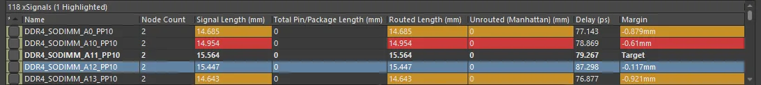
デフォルトでは、各xSignalに対して次の情報が一覧表示されます。
-
 – この機能には2つの役割があります。
- 背景色 – xSignalに割り当てられた色(デザインスペースでxSignalを表す細い線の色)です。右クリックして、現在選択されているすべてのxSignalに対してChange xSignal Color を実行します。
- 表示チェックボックス – これを使用すると、現在選択されているかどうかに関係なく、常にxSignalを表示できます。
- Name – xSignalの名前。
- Node Count – このxSignal内のパッド総数。
- Routed Length – 配線を構成する配置済みのトラックおよび円弧セグメントの長さの合計に、ビアを通過する垂直距離(下記注記参照)を加えたものです。配線長計算では、重なり合うトラックセグメントや、パッド内の配線のうねり(wiggles)を解決しようとはしません。
- Signal Length – ノード間の総距離を正確に計算します。信号長の計算には次の注記が適用されます。
- パッド内の重なりやうねりを解決します。
- トラックや円弧以外のオブジェクト(例:リージョンやフィル)で作成された配線パスを扱えます。
- ビアを通る垂直距離を含みます(下記注記参照)。
- このxSignalのTotal Pin/Package Lengthを含みます。
- このxSignalのUn-Routed (Manhattan) Lengthを含みます。
-
適用されるLength/Matched Lengthデザインルールに準拠していない場合、信号長が色付き背景で表示されてフラグ付けされます。短すぎる信号長は黄色、長すぎる信号長は赤で表示されます。
- Total Pin/Package Length – そのxSignal内のすべてのパッドにおけるPin Package Length値の合計です。この値はPCBパッドのプロパティとして定義され、回路図のピンでも指定できます。
- Unrouted (Manhattan) Length – 未配線区間すべての垂直+水平(X+Y)距離。
- Margin – 実際の信号長と、適用されるLength/Matched Lengthデザインルールで定義された目標信号長との差。
領域内で右クリックし、Columnsサブメニューを使用して次の列を追加します。
- Delay – 信号がその配線に沿って伝搬するのにかかる時間。
xSignalプリミティブ領域
PCBパネルの第3領域であるxSignal Primitivesには、現在選択されているxSignalの構成要素(プリミティブ)がすべて一覧表示されます。
領域のShow nodes onlyチェックボックスを選択すると、プリミティブの一覧をxSignalの開始/終了点ノードであるパッドに限定できます。このモードでは、選択したxSignalは、PCBデザインスペース上でノードパッド同士が細いトレース(トラックではない)で結ばれた形で表示され、これがxSignalパスを表します。
と、それぞれの遅延が一覧表示されます。")
下段のxSignal Primitives領域には、選択したxSignalのすべての要素(パッド、ビア、トラックなど)と、それぞれの遅延が一覧表示されます。
デザインスペースでのxSignal表示
xSignalはデザインスペース上で細い線として表示されます。この線はxSignalがたどる経路を示します。線の全長は、そのxSignalの信号長に対するX/Y成分です。全体の信号長に対するZ(垂直)成分は上で説明したとおりです。
下の画像では、差動ペアのxSignalが示されています。ペアのうち未選択のメンバーのxSignalも、パネルでそのxSignalのチェックボックスが有効になっているため表示されたままです。

xSignalはデザインスペース上で細い線として表されます。この差動ペアでは、パネルで1つしか選択されていなくても、表示チェックボックスが有効なため両方のxSignalが表示されたままです。
xSignalの削除
パネルでxSignalを選択し、xSignalリストの下にあるDeleteボタンをクリックします。あるいは右クリックしてコンテキストメニューからDeleteを選択するか、キーボードでDeleteを押します。
xSignalクエリキーワード
PCBエディタには、強力で高度なfiltering engineが含まれています。このエンジンは、デザインスペースでオブジェクトを検索する際、対話的/自動の設計タスク中にルールを適用する際、そしてルール準拠をチェックする際に、オブジェクトを特定するために使用されます。設計者は、フィルタリングエンジンが認識するクエリキーワードを用いてクエリを記述し、関心のあるオブジェクトをフィルタリングエンジンに指示します。
設計ルールおよびデザインスペースフィルタで使用するために、次のxSignalタイプのクエリキーワードが追加されています。
所属チェック型キーワード
- InxSignal - 指定したxSignalにオブジェクトが含まれているか(例:
InxSignal('DRAM_A0_PP1') - InxSignalClass) - 指定したxSignalクラスにオブジェクトが含まれているか(例:
InxSignalClass('PCIE') - IsxSignal) - 指定した名前のxSignalであるか(例:
IsxSignal('DRAM_A0_PP1')
)IsxSignal('DRAM_A0_PP1')
属性チェック型キーワード
- InAnyxSignal - いずれかのxSignalにオブジェクトが含まれているか(例:
InAnyxSignal
)InAnyxSignal
xSignalに対するデザインルールのサポート
デザインルールは、要件をPCBエディタが理解して遵守できる指示セットへ変換する方法です。ルールは、オブジェクト配置中(Online DRC)にチェックすることも、後処理(Batch DRC)としてチェックすることもできます。xSignalは、デザインルールを適用すべきオブジェクトを定義するために使用できます。
Matched Lengthルール
Matched Length デザインルールは、指定したネットの長さが指定範囲内に収まることを保証するために使用します。このルールは高速設計において不可欠です。高速設計での課題は、信号が到達するまでの時間(全体の配線長で決まる)だけではなく、指定した信号が同時に到達することがどれほど重要か、という点にあります。信号のスイッチング速度、信号の役割、基板で使用する材料によって、許容差は500 mils程度になる場合もあれば、1 mil程度しか許されない場合もあります。
下の画像は、xSignalクラスPCIE内のxSignalsをターゲットにするよう設定したMatched Lengthデザインルールの例で、同クラス内の各差動ペアについて、ペア内の長さ差をテストします。クラス内の各ペアは、ペア内2つのネット間のDelay Toleranceが2ps delay以下となる配線長でルーティングされている必要があります。
か、ターゲットネット内の各差動ペアの2ネットを一致させるか、いずれかを選択する必要がある点に注意してください。")
Matched LengthデザインルールのConstraintsでは、ターゲットとなる全ネットの長さを一致させる(Group Matched Lengths)か、ターゲットネット内の各差動ペアの2ネットを一致させるか、いずれかを選択する必要がある点に注意してください。
下の画像は、パネルでPCIE_TX xSignalクラスを選択し、設計空間でそれらのxSignalsを選択している例です。

PCIEクラスに加えて、TXおよびRXペア用のクラスも定義されています。TX xSignalsのうち1つが、適用されるマッチド長ルールに違反している点に注意してください。 ##
単一ネットと差動ペアの両方を含むxSignalsを長さ調整する予定がある場合、次のルールを作成してください。
- 長さ一致要件を定義するMatched Lengthルールbetween nets and differential pairs in xSignals。あるネット/ペアの長さを別のネット/ペアの長さと比較してテストするように設定するには、Group Matched Lengths オプションを有効にします。
- 2つ目として、優先度がより高いMatched Lengthルールを作成し、within-pair の長さ一致要件を定義します。ペアの片側メンバーをもう片側メンバーと比較してテストするように設定するには、Within Differential Pair Length オプションを有効にします。
このようなxSignalsの長さを調整するための良い手順は次のとおりです。
- xSignalのネットおよび差動ペアを配線します。
- Interactive Length Tuning コマンドを使用して単一ネットを長さ調整します。
- between のペアをInteractive Differential Pair Length Tuning コマンドで長さ調整します。長さ調整では、最長ペア内の最長信号長をTarget Lengthとして使用し、ペア内の最長ネットをこの長さに合わせて調整します。
- within 短い方のネットを、Interactive Length Tuning コマンドを使用して、各ペア内で相手側ネットに対して長さ調整します。
- 次に、PCB Rules and Violations パネルを使用してwithin-pair Matched Net Lengthルールを確認できます。これを行うには、パネルのRule Classes セクションでMatched Net Lengths を選択し、必要なMatched Length ルールを右クリックして、コンテキストメニューからRun DRC Rule <RuleName> コマンドを選択します。必要に応じて単一ネットのチューニング用アコーディオンを調整します。
- 続いて、同様にPCB Rules and Violations パネルを使用してbetween-pair Matched Net Lengthルールを確認します(上で説明した手順を使用)。必要に応じて差動ペアのチューニング用アコーディオンを調整します。
Length Rule
Length デザインルールは、全体の配線長が指定範囲内に収まることを保証するために使用します。このルールは通常、ターゲットネットが指定長より長くならないことを保証するために使用します。たとえば、回路のタイミング要件が満たされることを保証する目的です。Lengthルールは、上記に示したxSignalタイプのクエリを考慮します。
Return Path Rule
Return Path デザインルールは、ルールがターゲットとする信号の上または下にある指定参照層に、連続した信号リターンパスが存在するかをチェックします。リターンパスは、信号層上に配置されたフィル、リージョン、ポリゴンポアから作成でき、またはプレーン層でも構いません。
リターンパス層は、選択したImpedance Profileで定義される参照層です。High Speedルールカテゴリで新しいReturn Pathデザインルールを追加します。
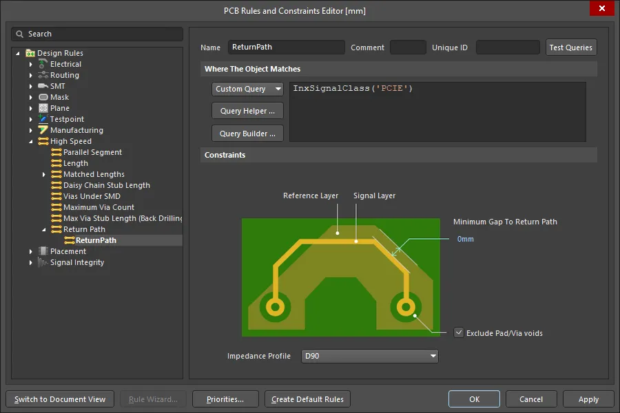
下の画像はReturn Pathルール違反の例で、xSignalのリターンパスポリゴンに、ビアが通過するための穴が開いています。
 PCB Rules and Violationsパネルを使用してReturn Pathルール違反を特定します。 ##
Accurate Length Calculations
高速設計ルールを定義するうえでの重要要件は、配線長を正確に計算することです。従来の信号長計算の方法は、配線に使用されたすべてのセグメントの中心線長を合計し、さらにビアの高さによる垂直距離(元々は基板厚で決めていた)を加算する、というものです。
しかし、この方法は以下の理由などにより高速設計には不十分です。
- 積層・重なり合うオブジェクト - ネット内のすべてのオブジェクトの中心線長を単純に加算するアルゴリズムでは、積層や重なり合いに対応できません。
- オブジェクト内での配線経路の蛇行 - パッドやビアの内部に完全に含まれる配線オブジェクトが存在することが多く、下の最初の画像に示すように、誤って長さが加算される場合があります。2枚目の画像は、フィルオブジェクトが配線の一部である場合に、正しく長さを計算する方法を示しています。
- ビア長 - ブラインドビアや埋め込みビアは基板の全層を貫通しないため、基板厚だけでは垂直長を十分に正確に求められません。ビアが通過する銅厚および絶縁厚を考慮し、実際のビア高さを使用する必要があります。
PCBエディタの長さ計算機能は、可能な限り最も正確な配線長を返します。

長さ計算は、これら2つの画像に示すように、最短経路の中心線に沿って正確に計算されます。

ビアについては、通過する層とスタックアップ寸法に基づいて正確な長さが計算されます。画像はPCBパネルのNetsモードからのものです。
Pin Package Delay
500 MHzを超えるすべての高速設計では、接続媒体(ダイへのボンドワイヤ)が信号に遅延を導入します。このデバイス内部の遅延は、ピン・パッケージ遅延(pin-package delay)と呼ばれます。設計およびPCBの観点で2つのデバイスが完全にピン互換であっても、パッケージのフライトタイムはデバイス間で異なるため、考慮する必要があります。フライトタイム情報は、そのデバイスのIBIS 6ドキュメント内で確認できます。Package Pins情報は、I/Oプランニング段階、またはFPGAであれば合成後に考慮すべきです。すべてのデバイスメーカーはパッケージ遅延を提供できるはずで、ピコ秒の遅延または長さとして指定されます。
遅延は、設計にPin Package LengthまたはPropagation Delayとして含めることができ、回路図エディタのピン、またはPCBエディタのパッド/ビアの各フィールドを使用して設定します。入力した値は次のように扱われます。
Pin Package Length - 各ネット内のすべてのピン・パッケージ長はPCBエディタで加算され、Total Pin/Package Lengthとなり、そのネットの全体Signal Lengthに含まれます。PCBパネルのNetsモードを参照して、Signal Lengthについて詳しく学んでください。
Propagation Delay - 各ネット内でピン/パッドおよびビアに対してユーザー定義された遅延値はすべて、PCBエディタでそのネットの配線遅延に加算されます。配線遅延は、Layer Stack Managerに組み込まれたSimbeor®フィールドソルバによって自動計算されます。パッドおよびビアの遅延は自動計算されませんが、ユーザー定義できます。
Including the Delay in the Schematic
ピン・パッケージ長は、PinモードのPropertiesパネルで、回路図コンポーネントのピン属性として定義できます。ソフトウェアは基になるドキュメントのUnitsをデフォルトで使用します。必要に応じて、値とともに単位を入力してください。

必要な単位でピン・パッケージ長を入力します。
 をクリックして
PCBエディタで遅延を定義する
ピンのパッケージ長(Pin Package Length)と伝搬遅延(Propagation Delay)の値は、PropertiesパネルのPadモードに示されるようにPCBレイアウトへ転送されます。

ピンのパッケージ長と伝搬遅延の値は回路図からPCBへ転送されますが、PCB側で直接定義することも可能です。
PCBパネルでピン/パッケージ長と伝搬遅延を確認する
Pin/Pkg LengthはSignal Lengthの計算に自動的に含まれ、その結果はPCBパネルの各種モードで表示されます。パネルをNetsモードに設定すると、選択したネット内のピンに対するPin/Pkg Lengthの値を確認(または編集)できます。Routed Length列が配線(ルーティング)の長さを反映し、Signal Length列が配線長に加えてそのネット内のPin/Pkg Lengthを含めた長さを反映している点に注目してください。

Pin/Pkg Lengthと、それがSignal Lengthに与える影響は、PCBパネルのNetsモードに表示されます。
下の画像では、伝搬Delay列が、Matched Lengthデザインルールに不合格となっているxSignalsのペアが2組あることを示しています。ハイライトがDelay列に出ているため、このルールがLength UnitsではなくDelay Unitsを使用するよう設定されていることが分かります。
 Delay列は、Matched Lengthデザインルールに不合格となっているxSignalsのペアが2組あることを示しています。
xSignalsに長さが含まれる仕組み
Pin/Pkg Lengthは、次の場合に全体のxSignal長へ自動的に含まれます。
- その信号がxSignal定義の一部である
- そのパッドがフライバイ配線パターンで接続されていない(そのパッドに接続されるトレースが1本のみ)
ネット関連の用語
PCBエディタでは、次の用語が使用されます。
- Net – 相互に接続されたコンポーネントのピン(ノード)の集合。これらのノードがどのように接続されるかという配置はトポロジーと呼ばれ、デフォルトのトポロジーは最短です。
- From-To – 概念的には、From-Toはネット内の2つのノード間を結びます。From-Toは、そのネット内のトポロジー(ノードの配置)に従うように作成できます。たとえば、ネットのトポロジーがR1-1→U1-5→U3-2→R5-2である場合、このネットには3つのFrom-To(R1-1→U1-5、U1-5→U3-2、U3-2→R5-2)を持たせることができます。トポロジーを変更すると、作成可能なFrom-Toも変わります。From-Toは、PCBパネルのFrom-Toモードで、Generateボタンをクリックしてトポロジーに基づいて作成するか、ネット内の2つのパッドを選択してからAdd From Toボタンをクリックして作成します。
- xSignal – ユーザー定義のノード集合。通常はネットのサブセット(このノードからあのノードまで)であるか、終端抵抗のような直列部品を含む2つのネットの組み合わせです。
 AI で翻訳