回路図ドキュメントの作成とチェックの後の論理的なステップは、PCB の作成と設計です。新しい PCB ドキュメントを作成するには、 File " New " PCB コマンドを使用します。原点、単位、グリッドサイズ、必要なレイヤの色表示や可視性を定義することで PCB を設定するのは良い考えです。
PCB 環境設定の多くの側面は、後述するBoardモードのPropertiesパネルを通して設定されます。PCB 環境設定の他の機能については、以下のページを参照してください:
-
Cursor-Snap System での作業- PCB エディタは、デザインオブジェクトの正確な位置や整列を助けるために設計された多くのスナップ機能を含みます。スナップグリッドシステムを補完するのはホットスポットスナップ機能で、スナップグリッドを上書きし、カーソルがユーザー定義可能な範囲内にある時、オブジェクトのホットスポットに引き寄せます。この機能により、グリッドから外れたオブジェクト、例えばメートル基板上のインペリアル・コンポーネントのパッドまでの配線が容易になります。これらの機能を合わせて、ユニファイド・カーソルスナップ・システムと呼びます。
-
グリッドとガイドでの作業- PCB エディタはグリッドベースのデザイン環境です - デザインオブジェクトは、配置、またはスナップグリッドと呼ばれるものに配置されます。ユーザ定義可能なスナップポイントやスナップガイド、オブジェクト軸のアライメントガイドもあり、オブジェクトの正確な位置決めに役立ちます。
-
PCB のビュー- 現代の PCB は、PCB エディタデザインスペースで明確に表現する必要があるマルチレイヤーエンティティです。Altium Designer は、2Dと3Dの両方のモードで、今必要なオブジェクト、レイヤ、ネットの表示を容易にするツールの包括的なセットを備えています。
-
PCB パネル-PCBパネルは、どのオブジェクトタイプやデザイン要素がリストされるか、ハイライトされるか、選択されるかを決定するために、様々なフィルタモードを使用して現在の PCB デザインをブラウズできます。
Properties パネル
BoardモードのPropertiesパネル(PCB エディタデザインスペースでデザインオブジェクトが現在選択されていない時にアクティブ)は、現在の PCB ドキュメントの基本的な設定のためのオプションやコントロールを含みます。
以下の折りたたみ可能なセクションは、パネルのGeneralタブで利用できるオプションやコントロールに関する情報を含みます:
-
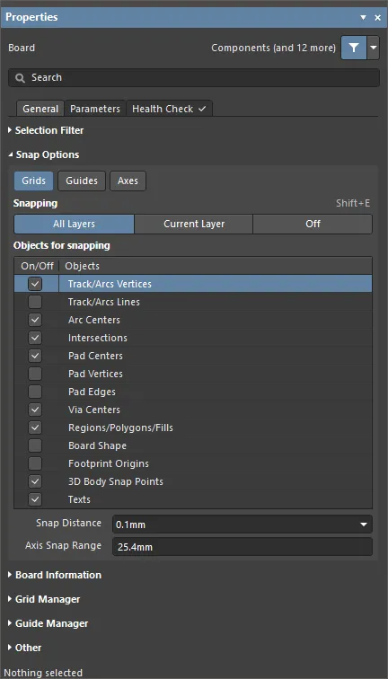
Grids- カーソルをアクティブなデザインスペースのグリッドにスナップするかどうかを切り替えます。このオプションが有効な場合、カーソルは最も近いスナップグリッド位置にプル、またはスナップします。アクティブなスナップグリッドは、Status バー、PCB エディタの Heads Up 表示に表示されます。
-
Guides- 手動で配置したリニアまたはポイント Snap Guide にカーソルをスナップするかどうかを切り替えます。Snap Guide は Snap Grid を上書きします。
-
Axes- カーソルがスナップするために有効なObjectsに(XまたはY方向に)軸を合わせるかどうかを切り替えます。Axis Snap Range(軸スナップ範囲)は、X軸またはY軸のアライメントが発生する距離を定義します。アライメントが達成されると、現在のカーソル位置から軸方向にアライメントされたオブジェクトスナップポイント(ホットスポット)まで、ダイナミックアライメントガイドラインが表示されます。
-
スナップ- 直接選択するか、Shift+Eのショートカットを使用して、オブジェクトにスナップするかどうかを選択します:
-
All Layers- このオプションを有効にすると、カーソルが表示されているレイヤー上の電気オブジェクトにスナップできるようになります。
-
現在のレイヤー- このオプションを有効にすると、カーソルは現在選択されているレイヤー上のオブジェクトのみを認識し、スナップすることができます。
-
オフ- このオプションを有効にすると、ホットスポットへのスナップがオフになります。
-
スナップするオブジェクト
-
On/Off- 必要なオブジェクトのスナップを有効にする場合はチェックします。
-
Objects- 利用可能なオブジェクトのリストです。
-
スナップ距離- カーソルが有効なオブジェクトスナップポイントからこの距離内にある場合(アクティブレイヤーでスナップが有効な場合)、カーソルはそのポイントにスナップします。
-
Axis Snap Range(軸スナップ範囲) - カーソルが有効なオブジェクトスナップポイントからこの距離内にある時(そしてAxes機能が有効な時)、ダイナミックガイドラインが表示され、アライメントが達成されたことを示します。
[折りたたみ]
ボード情報
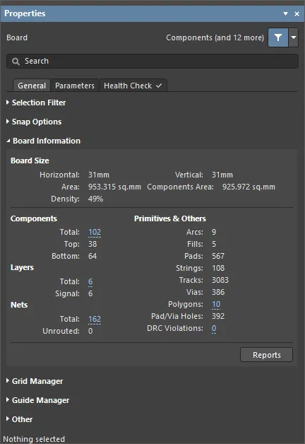
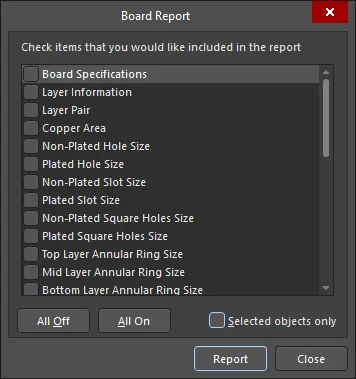
サポート対象は以下の通り:
-
基板の仕様- 基板のサイズと基板上の部品数に関する一般的な情報。
-
Layer Information(レイヤー情報) - プリミティブ(円弧、パッド、ビア、トラック、テキスト、フィル、リージョン、コンポーネントボディ)が基板の各使用レイヤーにいくつあるか、各プリミティブタイプの合計使用量と共に。
-
Layer Pair(レイヤーペア) - 定義されたドリルレイヤーペアと、それらのペア間で開始および停止するビアの数の内訳。
-
銅エリア- オブジェクト(ボード領域、ボード形状、ポリゴン注入など)の銅エリアを含むレイヤーの数、銅エリアのサイズ(インチとミリメートルで提供)、および各レイヤー内で使用される銅エリアの割合。
-
Non-Plated Hole Size- このタイプの各ホールサイズのパッドとビアの数。
-
メッキホールサイズ - このタイプの各ホールサイズに対応するパッドとビアの数。
-
Non-Plated Slot Size(非メッキ・スロット・サイズ) - このタイプの各スロット・サイズに対応するパッド数。
-
メッキスロットサイズ- このタイプの各スロットサイズのパッド数。
-
非メッキ角穴サイズ- このタイプの各穴サイズに対応するパッド数。
-
メッキ角穴サイズ- このタイプの各穴サイズに対応するパッド数。
-
トップレイヤー環状リングサイズ- トップレイヤーの各環状リングサイズに対応するオブジェクト(パッドとビア)の数。
-
ミッドレイヤー・アニュラー・リングサイズ- ミッドレイヤーの各アニュラー・リングサイズのオブジェクト(パッドとビア)の数。
-
ボトムレイヤー・アニュラー・リングサイズ - ボトムレイヤーの各アニュラー・リングサイズのオブジェクト(パッドとビア)の数。
-
Pad Solder Mask(パッド・ソルダー・マスク) - 指定された一意のソルダー・マスク拡張値ごとのパッド数。
-
Pad Paste Mask (パッド・ペースト・マスク) - 指定された一意のペーストマスク拡張値ごとのパッド数。
-
Pad Pwr/Gnd Expansion- 定義された電源プレーンのクリアランスルールで指定された固有のクリアランス 値に関連するパッド数。
-
パッドリリーフ導体幅- 定義された電源プレーンの接続スタイル規則で指定された固有の導体幅値に関連するパッドの数。
-
パッドリリーフエアギャップ- 電力プレーンの接続スタイル規則で指定されたエアギャップ値に関連するパッドの数。
-
パッドリリーフエントリ- 電力プレーンの接続スタイル規則で指定された固有のコンダクタ値に関連するパッドの数。
-
Via Solder Mask (ビアはんだマスク) - 指定された固有のはんだマスク拡張値ごとのビア数。
-
Via Pwr/Gnd Expansion- 定義された電源プレーンのクリアランスルールで指定された固有のクリアランス 値に関連するパッド数。
-
Track Width (トラック幅) - デザインで使用される固有のトラック幅のオブジェクト数。
-
Arc Line Width(弧線幅) - デザインで使用される固有の弧線幅ごとのオブジェクト数。
-
Arc Radius- デザインで使用される各円弧半径に対応するオブジェクトの数。
-
Arc Degrees- デザインで使用される各ユニークな円弧角度のオブジェクト数。
-
Text Height(テキストの高さ) - デザインで使用される固有のテキストの高さに対応するオブジェクトの数。
-
Text Width- デザインで使用される各テキスト幅のオブジェクト数。
-
ポリゴンクリアランス - デザインで使用される各クリアランスのポリゴン数。
-
Net Track Width(ネット・トラック幅 ) - 設計に使用された各幅のネット・トラックの数。
-
Net Via Size - デザインで使用される各サイズのネット ビアの数。
-
Routing Information (配線情報)- 配線完了の情報 (パーセンテージ)、コネクションの総数、配線済み数、残り数の内訳。
Selected objects onlyオプションを有効にすると、メイン・デザイン・スペースで現在選択されているデザイン・オブジェクトに関してのみ、各インクルード・アイテムの情報をレポートが生成します。このオプションを使用するには、デザインスペースで必要なオブジェクトを選択し、PCB エディタのReports メニューからダイアログにアクセスする必要があります。
-
レポートに含めるために必要な項目がすべて有効になったら、 レポート ボタンをクリックしてレポートを作成します。
-
レポートは、PreferencesダイアログのPCB Editor - Reports ページの設定に従って、Text や HTML フォーマットで生成されます。
-
レポートファイルは、.txtまたは.htm という名前で、PCB ファイルと同じフォルダに作成されます。HTML バージョンは、HTML Title,Board Information Report です。
です。
Click here to expand or collapse this section

-
Grid Manager- ローカルにカスタマイズされたグリッドを定義、管理することができます。
-
Priority- デザインスペースで、優先順位は描画順序によって区別されます。最も優先度の高いグリッド(優先度
1)は、他のすべてのグリッドの前に描画され、次に優先度2のグリッドなど、デフォルトのグローバルボードスナップグリッドまで、他のすべてのカスタムグリッドの後ろに描画されます。
-
Name- グリッドの名前を表示します。
-
色- クリックするとドロップダウンが開き、関連するグリッドの色を設定/変更できます。
-
Origin- デザイン空間に原点マーカーを表示します。
-
Comp- 選択したグリッドをコンポーネントのみに適用します。
-
Non Comp- 選択したグリッドをコンポーネント以外のオブジェクトに適用します。
-
追加
-
Add Cartesian Grid- クリックしてデカルトグリッドを追加します。
-
Add Polar Grid- クリックしてポーラーグリッドを追加します。ポーラーグリッドを使用すると、非矩形のフィーチャーやボードをより簡単に設計できます。
-
Properties- クリックすると、それぞれのグリッドエディタダイアログ(Cartesian Grid EditorまたはPolar Grid Editor)が開き、選択したグリッドのプロパティを変更できます。
-
 - クリックすると、現在選択されているグリッドが削除されます。
。

-
Guide Manager- ここで、ボードのマニュアルスナップガイドとスナップポイントの範囲を定義し、管理することができます。
-
追加- クリックして新しいスナップガイドまたはスナップポイントを追加します。関連するメニューから必要なガイドタイプに対応するコマンドを選択すると、新しいガイド/ポイントのエントリがグリッドに追加されます。以下のガイドタイプがあります:
-
水平ガイドを追加- このコマンドを使用して、デザインスペースの必要なY座標位置に水平ガイドを追加します。
-
垂直ガイドを追加- このコマンドを使用して、デザイン空間の目的のX座標位置に垂直ガイドを追加します。
-
Add +45 Guide- このコマンドを使用して、デザイン空間の目的のX,Y座標位置を通る45度(y=x)のガイドラインを追加します。
-
Add -45 Guide-このコマンドを使用して、デザイン空間の目的のX,Y座標位置を通る-45度(y=-x)のガイドラインを追加します。
-
Add Snap Point- このコマンドを使用して、点スナップガイドを追加します。これは、デフォルトのスナップグリッドの範囲内で手動でマークするホットスポットです。オブジェクトの配置や移動などのインタラクティブな処理中に、そのオブジェクトのホットスポットがポイントスナップガイドの近くを通過すると、ポイントスナップガイドに「スナップ」します。
-
配置- クリックしてガイドを配置します。ドロップダウンからガイドタイプを選択します:
-
水平ガイドを配置]-このコマンドを使用して、デザイン空間の目的のY座標位置に水平ガイドを配置します。
-
Place Vertical Guide(垂直ガイドを配置)-このコマンドを使用して、デザインスペースの希望のX座標位置に垂直ガイドを配置します。
-
Place +45 Guide- このコマンドを使用して、デザイン空間の目的のX,Y座標位置を通る45度(y=x)のガイドラインを配置します。
-
Place -45 Guide-このコマンドを使用して、デザイン空間の目的のX,Y座標位置を通る-45度(y=-x)のガイドラインを配置します。
-
Place Snap Point- このコマンドを使用して点スナップガイドを配置します。これは、デフォルトのスナップグリッドの範囲内で手動でマークするホットスポットです。オブジェクトの配置や移動などのインタラクティブな処理中に、そのオブジェクトのホットスポットがポイントスナップガイドの近くを通過すると、ポイントスナップガイドに「スナップ」します。
-
- クリックすると、現在選択されているガイドが削除されます。
ガイドは、[表示設定]パネル(show image![]() ) の [表示オプション]タブで [グリッドを表示]オプションが有効になっている場合にのみ表示されます。
) の [表示オプション]タブで [グリッドを表示]オプションが有効になっている場合にのみ表示されます。
[折りたたみ]
-
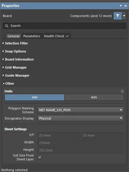
Units- 現在の PCB ドキュメントのデフォルトの測定単位を選択します。デフォルト単位は、画面上またはレポート内の距離関連情報を表示するために使用されます。デフォルト単位は、距離関連情報を指定する時に単位の接尾辞(mm または mil)が入力されない場合、常に使用されます。
-
View " Toggle Units を選択(またはQショートカットを押す)して、デザインスペースの単位をインペリアルとメトリックに切り替えます。
-
ダイアログやパネルがアクティブなときにCtrl+Q を押すと、そのダイアログやパネル内のすべての測定単位が切り替わります。
-
単位の現在の設定に関係なく、ダイアログやパネルで値を入力するときに単位を含めると、その値が強制的に使用されます。
-
ポリゴン命名法- ドロップダウンメニューから命名法を選択します。命名テンプレートには4つの選択肢があります:
-
ネット名_lxx_pxxx
-
lxx_ネット名_pxxx
-
ネット名_レイヤ名_pxxx
-
レイヤー名_ネット名_pxxx
ここで
-
NET NAME- ポリゴンが接続されているネットの名前。ポリゴンがネットに接続されていない場合、NONETという名前が使用される。
-
LAYER NAME(レイヤー名) -レイヤースタックからユーザーが定義したレイヤー名。
-
LXX- トップレイヤーがL01であるレイヤースタックの現在のレイヤーの順番に基づき、システムが割り当てた銅レイヤー番号。この値は、銅レイヤーの順序が変更されるたびに更新されます。
-
PXXX- システムが割り当てた数値インデックス。ボード上の各ポリゴンに一意。
レイヤスタック内のレイヤの移動、ネット名の変更、命名スキームの変更などのデザイン変更により、名前が自動的に変更されます。影響を受けるデザイン・ルールは自動的に更新されます。
-
Designator Display- このフィールドを使用して、デジグネータの表示方法を決定します。デジグネータの文字列は非常に長くなるため、マルチチャンネル・デザインでは配置が難しい場合があります。短い名前になるネーミング・オプションを選択するだけでなく、元の論理的なコンポーネントの名称だけを表示することもできます。例えば、C30_CIN1はC30と表示される。この場合、もちろん、コンポーネント・オーバーレイ上で各チャンネルを囲むボックスが描かれるなど、個別のチャンネルを示す他の表記をボードに追加する必要があります。以下のオプションが利用可能です:
-
Physical- 物理デジグネータの表示を選択します。これらは、回路図ソース・ドキュメントのコンパイルされたタブ・ビューに表示されるデジグネータです。マルチチャンネルデザインの場合、デジグネータのフォーマットはProject OptionsダイアログのMulti-ChannelタブにあるDesignator Formatフィールドによって決定されます。物理的なデジグネータはR1_CH1 のように一意です。
-
Logical- 論理的なデジグネータを表示します。これは、回路図ソースドキュメントのEditorタブビューに表示されるデジグネータです。論理デジグネータは一意ではありません。例えば、R1_CH1物理デジグネータは単にR1 になります。
-
Sheet Settings- PCB シートを設定するためにこの領域を使用します。
-
X/Y- シートの左下隅の X 座標と Y 座標を入力します。この距離は、デザインスペースの左下隅である絶対原点から測定されます。距離は、デフォルトの単位(Units設定で決定される)に関係なく、メートル単位またはインペリアル単位で定義できます。サイズを入力する際に単位を指定するには、値に mm または mil の接尾辞を追加します。
-
幅- ここにシートの幅を入力します。シートは、従来の図面シートを模した領域を提供し、寸法、注記、タイトルブロックなどの情報を配置するのに便利です。機械レイヤーに配置された情報は、シートが表示されているときのみ表示されるように、シートにリンクさせることができます。シートサイズは、デフォルトの単位(単位設定により決定される)に関係なく、メートル単位またはインペリアル単位で定義できます。サイズを入力する際に単位を指定するには、値に mm または mil の接尾辞を追加します。
-
高さ- ここにシートの高さを入力します。シートは、従来の図面シートを模した領域を提供し、寸法、注記、タイトルブロックなどの情報を配置するのに便利です。機械レイヤーに配置された情報はシートにリンクすることができ、シートが表示されているときのみ表示されます。シートサイズは、デフォルトの単位(単位設定により決定される)に関係なく、メートル単位またはインペリアル単位で定義できます。サイズを入力する際に単位を指定するには、値に mm または mil の接尾辞を追加します。
-
シートレイヤーからサイズを取得- このオプションを有効にすると、シートレイヤーからシートのサイズを設定できます。
[折りたたみ]
以下の折りたたみ可能なセクションには、パネルのParameterタブで使用できるオプションとコントロールに関する情報が含まれています:
Strings
以下の折りたたみ可能なセクションには、パラメータ・タブで使用できるオプションとコントロールに関する情報が含まれています。
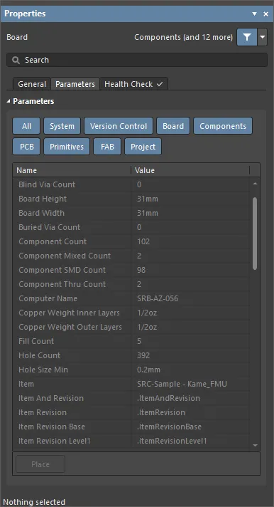
-
ボタン- 各ボタンを切り替えると、下のグリッド表に関連するパラメータの表示/非表示が切り替わります。
-
グリッド- 現在の PCB ドキュメントに関連するパラメータのNameとValue をリストします。グリッドは、システムパラメータ(例えば、PCB ファイル名)、PCB から計算されたパラメータ(例えば、PCB のコンポーネント数、基板の厚さ)の両方を一覧表示します。
-
Place- クリックして、現在選択されているパラメータを特殊文字列として配置します。特殊文字列は、PreferencesダイアログのPCB Editor - Defaults ページでテキストオブジェクトのデフォルトレイヤーとして定義されたレイヤーに配置されます。
[/collapse]
ヘルスチェック
パネルのHealth Checkタブは、PCB Health Check Monitor へのインターフェースを提供します。この機能の詳細については、PCB Health Check Monitor を参照してください。
オブジェクトが選択された時
デザインオブジェクトが選択されると、パネルはそのオブジェクトタイプに特有のオプションを表示します。以下の表は、PCB ドキュメント内で配置可能なオブジェクトタイプの一覧です - リンクをクリックすると、そのオブジェクトのプロパティページにアクセスできます。
Tracksと Linesは実際には同じオブジェクトですが、配置時のソフトウェアの動作が異なるため、コマンドが異なります。
Place " Lineコマンドを起動すると、カーソルは十字に変わり、エディタは線の配置モードになります。配置は以下の操作で行います:
-
クリックして線の開始位置を定義する。
-
カーソルを動かして線の長さと角度を設定し、もう一度クリックして配置を完了します。
-
さらに線の配置を続けるか、右クリックまたはEscキーを押して配置モードを終了します。

