A variety of objects are available for use in designing a PCB. Most objects placed in a PCB document will define copper areas or voids. This applies to both electrical objects, such as tracks and pads, and non-electrical objects, such as text and dimensioning. It is therefore important to keep in mind the width of the lines used to define each object and the layer on which the object is placed.
There are two types of objects in the PCB editor – primitive objects and group objects. Primitive objects are the most basic elements and include: tracks, pads, vias, fills, arcs, and strings. Anything that is made up of primitives and identified as a design object is a group object. Examples of group objects include: components, dimensions, coordinates, and polygon pours.
Object Placement and Editing Commonality
In Altium NEXUS, the process of placing an object is roughly the same regardless of the object being placed. At its simplest level, the process is as follows:
- Select the object to be placed from one of the toolbars or the Place menu.
- Use the mouse to define the location of the placed object in the PCB editor design space and its size (where applicable).
- Right-click (or press Esc) to terminate the command and exit placement mode.
Editing Prior to Placement
The default properties for an object can be changed at any time on the PCB Editor – Defaults page of the Preferences dialog. These properties will be applied when placing subsequent objects..

Use the Primitives column to access properties for objects and edit default values as required.
Default values for the objects are saved, by default, in the file ADVPCB.dft. Optionally, values can be saved in a .dft file with a different name. Controls are available to save and load .dft files, enabling you to create favorite default object value 'sets'. All settings saved in and loaded from .dft files are user-defined defaults. Should it be necessary, original default values can be brought back at any time using the Set To Defaults or Reset All options. The original default values are hard-coded.
Editing During Placement
A number of attributes are available for editing at the time an object is first placed. To access these attributes, press the Tab key while in placement mode to open the associated Properties panel. Pressing the Tab key pauses placement in order for you to make any required edits for the object.

Example properties dialog for a Pad object.
After edits have been made, click the design space pause button overlay (  ) to resume placement.
Attributes that are set in this manner will become the default settings for further object placement unless the
Permanent option on the
PCB Editor – Defaults page of the
Preferences dialog is enabled. When this option is enabled, changes made will affect only the object being placed and subsequent objects placed during the same placement session.
Editing After Placement
Once an object has been placed, there are a number of ways in which it can be edited. These are described below.
The Associated Properties Panel or Dialog
This method of editing uses the associated Properties panel mode and dialog to modify the properties of a placed object.
After placement, the associated dialog can be accessed by:
- Double-clicking on the placed object.
- Placing the cursor over the object, right-clicking then choosing Properties from the context menu.
After placement, the associated mode of the Properties panel can be accessed in one of the following ways:
- If the Properties panel is already active, select the object.
- After selecting the object, select the Properties panel from the Panels button at the bottom right of the design space or select View » Panels » Properties from the main menus.
If the
Double Click Runs Interactive Properties option is disabled (default) on the
PCB Editor – General page of the
Preferences dialog, when the primitive is double-clicked or you right-click on a selected primitive then choose
Properties, the dialog will open. When the
Double Click Runs Interactive Properties option is enabled, the
Properties panel will open.
While the options are the same in the dialog and the panel, the order and placement of the options may differ slightly.
Press Ctrl+Q to toggle the units of measurement currently used in the panel/dialog between metric (mm) and imperial (mil). This only affects the display of measurements in the panel/dialog; it does not change the measurement unit specified for the board, which is configured in the Units setting in the Properties panel when there are no objects selected in the design space.
Graphical Editing
This method of editing allows you to select a placed object directly in the design space and change its size, shape, or location graphically. Modification of shape and/or size (where applicable) is performed through the use of editing 'handles' that appear once the object is selected.
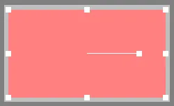
Example editing handles for a selected Fill object.
Click anywhere on an object away from editing handles (where they exist) to drag the object to reposition it. Depending on the type of object, it may be rotated and/or flipped while dragging.
- Press Spacebar to rotate the object counterclockwise or Shift+Spacebar for clockwise rotation. Rotation is in accordance with the value for the Rotation Step defined on the PCB Editor – General page of the Preferences dialog.
- Press the X or Y keys to flip the object along the X-axis or Y-axis where applicable.
The number of primitives displayed when dragging multiple selected objects is controlled by the
PCB.Rendering.MultiselectionDrag option in the
Advanced Settings dialog. The
Advanced Settings dialog is accessed by clicking the
Advanced button on the
System - General page of the
Preferences dialog. If any changes are made in the
Advanced Settings dialog, the software must be restarted in order for the changes to take effect.
Alignment Commands
Objects can also be moved by changing their alignment. To align objects with other objects, right-click on a selected object, then select Align. The alignment sub-menu contains a number of options for distributing selected objects.

For more information on the individual alignment options, see the AlignComponents command page.
Via the PCB List Panel
Panel Page: PCB List
The PCB List panel allows you to display design objects in tabular format, enabling quickly inspection and modification of object attributes. When used in conjunction with the PCB Filter panel, it enables you to display just those objects falling under the scope of the active filter – allowing the targeting and editing of multiple design objects with greater accuracy and efficiency.
Locking Design Objects
Design objects can be locked from being moved or being edited on the PCB document by enabling their Locked attributes. For instance, if the position or size of specific objects is critical, lock them. Locking can be done in the Properties panel by clicking on the padlock icon ( ) for the desired object(s) as shown in the following examples.


Examples of the Lock icon in the Properties panel in Component mode and Pad mode.
If you attempt to move or rotate a design object that has its Locked property enabled, a dialog appears asking for confirmation to proceed with the edit.
If the Protect Locked Objects option is enabled in the PCB Editor – General page of the Preferences dialog and the design object is locked, the object cannot be selected or graphically edited. Use the Lock icon on the Properties panel to unlock the object or disable the Protect Locked Objects option to graphically edit this object.
If you attempt to select locked objects along with other objects, only those objects that are unlocked can be selected and moved as a group when the Protect Locked Objects option is enabled.
Component Primitive Locking
If a PCB component has its primitives locked (the Primitives option in the Component mode of the Properties panel is in its  state), all or the most properties of these primitives cannot be modified using graphical (e.g., using drag-and-drop) and non-graphical (e.g., using the Properties or List panel) editing methods. This will help to prevent occasional changes of component primitives that can result in incorrect assembly and fabrication outputs.
To enable/disable the preventing modification of PCB component primitives functionality, use the
Protect Locked Primitives In Component option on the
PCB Editor – General page of the
Preferences dialog.
By way of an example, the Pad mode of the Properties panel is shown in the image below for a pad that is a constituent part of a PCB component that has its primitives locked. Note that all properties of the pad (except for Net and Testpoint properties) are dimmed and not available for editing. Note also that the  icon is shown at the far right of the pad's Component field, which denotes that the parent component has its primitives locked, and pad properties cannot be modified.
 for a pad of a PCB component that has its primitives locked (on the right).")
The Pad mode of the Properties panel (on the left) for a pad of a PCB component that has its primitives locked (on the right).
Re-Entrant Editing
The PCB Editor includes a powerful feature called re-entrant editing. This allows a second operation to be executed using keyboard shortcuts without the current operation being terminated. Re-entrant editing allows you to work more flexibly and intuitively. For example, consider starting to place a track and then realizing that another track segment must be deleted. There is no need to drop out of Interactive Routing mode. Press the E, D shortcut keys, delete the required track segment then press the Esc key to return to interactively routing the design.
Setting the PCB Cursor Appearance
By default, the PCB cursor is set as a small green 90 degree cross. This can be configured using the Cursor Type and Cursor Color settings, on the PCB Editor – General page of the Preferences dialog. For example, a large 90 degree cross that extends to the edges of the design window (Large 90 option) can be useful when placing and aligning design objects. Alternatively, a cross at 45 degrees (Small 45 option) might be useful if the 90 degree options are hard to see against grid lines.
Priorities When Pasting Objects
When an object is being pasted on a copper layer, and it overlaps a set of objects of different types when pasted, a net of the highest priority object will be assigned to the pasted object. The priorities are as follows (1 is the highest priority):
- Pad
- Fill
- Region
- Track
- Arc
- Via
- Polygon Pour
 pasted over a set of objects of different types with different nets assigned. Since the pad is the object of highest priority in this set, its net (Pad_Net) will be assigned to the pasted object. Hover the cursor over the image to see the result.")
A net of the highest priority object is assigned to a pasted object. Here is shown an object (track) pasted over a set of objects of different types with different nets assigned. Since the pad is the object of highest priority in this set, its net (Pad_Net) will be assigned to the pasted object. Hover the cursor over the image to see the result.
When an object is being pasted on a copper layer, and it overlaps a set of objects of the same type when pasted, a net of the object that is under the cursor when clicking to paste the object will be assigned.
 pasted over a set of objects of the same type (pads). Since pad 2 is the object that is under the cursor when clicking to paste the object, the net of this pad (Pad2_Net) will be assigned to the pasted object. Hover the cursor over the image to see the result.")
A net of the object under the cursor is assigned to a pasted object. Here is shown an object (track) pasted over a set of objects of the same type (pads). Since pad 2 is the object that is under the cursor when clicking to paste the object, the net of this pad (Pad2_Net) will be assigned to the pasted object. Hover the cursor over the image to see the result.
When a set of physically connected objects is being pasted on a copper layer, and objects of different types in this set overlap existing objects with different nets, a net of the highest priority object in this set will be assigned to all pasted objects. The above priorities are applied in this case.
 pasted over objects (vias) with different nets assigned. Since the fill is the object of highest priority in this pasted set, the net assigned to it (Via1_Net) will be assigned to each object in this set. Hover the cursor over the image to see the result.")
The net assigned to the highest priority object is assigned to the set of the physically connected objects. Here is shown a set of connected objects (from left to right: Fill, Region, Track, Arc, Via, Polygon Pour) pasted over objects (vias) with different nets assigned. Since the fill is the object of highest priority in this pasted set, the net assigned to it (Via1_Net) will be assigned to each object in this set. Hover the cursor over the image to see the result.
True Type Font Support
The PCB Editor offers the ability to use Stroke-based or TrueType fonts for text-related objects in a design (string, coordinate, and dimension text). Choice of font is made from within the associated Properties panel. Three Stroke-based font options are available - Stroke, Sans Serif, and Serif. The Default style is a simple vector font that supports pen plotting and vector photoplotting. The Sans Serif and Serif fonts are more complex and will slow down vector output generation, such as Gerber. The Stroke-based fonts are built into the software and cannot be changed. All three fonts have the full IBM extended ASCII character set that supports English and other European languages. When using TrueType fonts, TrueType and OpenType (a superset of TrueType) fonts fount in the \Windows\Fonts folder is available for use. The feature also offers full Unicode support.
Note that only detected (and uniquely named) root fonts will be available for use. For example, Arial and Arial Black will be available but Arial Bold, Arial Bold Italic, will not.
The PCB Editor – TrueType Fonts page of the Preferences dialog provides options for embedding TrueType fonts when saving a design and for applying font substitution when loading a design.
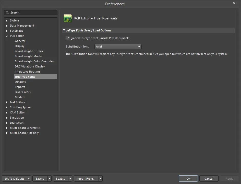
Embedding fonts is useful when text is required to be displayed in a font that may or may not be available on a target computer upon which the design is loaded. Font substitution enables specification of a TrueType font to be used as a replacement when loading a design where fonts have not been embedded and where fonts may not be available on the computer upon which the design is currently loaded.
Net Information
For copper objects on a PCB (track, via, polygon, etc.), the following information is presented in the Net Information region of the Properties panel when the object is selected:
- the parent Net, Diff Pair and/or xSignal and associated class in each case. Note that the Diff Pair and xSignal entries are shown only if the object is a part of a differential pair or xSignal, respectively.
- Delay – the delay of the selected object(s) and the delay of the routed segments of the entire net. Include the Propagation Delay values of pads and vias, if they have been defined for the pads and vias.
-
Length – the total length sum of the selected object(s) and the total Signal Length. The Signal Length is the accurate calculation of the total node-to-node distance. Placed objects are analyzed to: resolve stacked or overlapping objects and wandering paths within pads; and via lengths are included. The Pin Package Length is also included if it has been defined for the pad(s). If the net is not completely routed, the Manhattan (X + Y) length of the connection line is also included. For more information regarding Signal Length and its applications, see the information about the PCB - Nets panel.
The total length includes an estimate for the unrouted part of the net (the Manhattan (X + Y) length of the connection line), but for the total delay, it does not.
- For a selected Track, Arc or Via object, the calculated Max Current and Resistance values are also provided.

The Net Information region of the Properties panel. Shown here is an example for a selected track.
Click a link in the Net Information region to open the associated net/differential pair/xSignal in the PCB panel.
Primitive Objects
Primitive objects in the PCB Editor are fundamental elements of design. They are called 'primitive' due to their raw or most basic nature. Certain primitive objects are used as building blocks to create more advanced design objects, such as arcs, fills, and tracks, to create PCB 2D component models.
Primitive objects are available for placement in the PCB Editor, with many object types also supported for placement in the PCB Library Editor. Commands for placement can be found in the main Place menu, as well as the Active bar, the Utilities toolbar, and various drop-downs of the Wiring toolbar. Depending on the object, placement may require several mouse clicks to define the object's appearance.
 PCB primitive objects can be placed from the Active, Utilities, and Wiring toolbars.
Objects are placed on the current layer. Ensure the correct layer has been made the current layer before effecting placement. The layer on which an object resides can be changed after placement.
Track

Track objects are used for routing and for general-purpose drawing lines. There are four placed track segments in the image above, and another in the process of being placed.
A Track segment is a straight line of a defined width. Use tracks to define a straight line in the PCB design space. Tracks are placed on a signal layer to form the electrical interconnections, or routing, between component pads. Tracks placed on a non-electrical layer are called Lines, where they are used as general-purpose drawing elements to create component outlines, instructional information, keepout boundaries, etc. Tracks also are used in group design objects, such as dimensions and coordinates.
Tracks are available for placement in both PCB editor and the PCB Library editor. Regardless of which command is used (routing/track or line placement), the basic placement behavior is the same. After launching the command, the cursor will change to a crosshair and you will enter track placement mode. Placement is made by performing the following sequence of actions:
- Click or press Enter to anchor the starting point for the first track segment. If a routing-type placement command is being run and you click to start placement on an existing object, the track will adopt the net name of that object. For routing, the width will be determined by the applicable Routing Width design rule; this can be overridden by certain interactive routing options, which are described in more detail below.
- Move the cursor to define the track segment then click or press Enter to anchor the end point for this first segment, which is also the starting point for the next connected segment.
- Continue to position the cursor then click or press Enter to anchor a series of vertex points that define the series of connected track segments.
- Right-click or press Esc to end the current series of connected track segments.
While placing track segments there are five available corner modes, four of which also have corner direction sub-modes. During placement:
- Press Shift+Spacebar to cycle through the available corner modes.
- Press Spacebar to toggle between the two corner direction sub-modes.
- When in either of the arc corner modes, hold the , or . key to shrink or grow the arc. Hold the Shift key as you press to accelerate arc resizing.
- Press the 1 shortcut key to toggle between placing one segment per click (shown in the first five images below), or two segments per click (shown in the last image below). In the first mode, the hollow track segment is referred to as the look-ahead segment.
- Press the Backspace key to remove the last vertex.


Press Shift+Spacebar to cycle through the five available corner modes, press Spacebar to toggle the corner direction, press the 1 shortcut to toggle placement between one segment or two segments.
The graphical method of editing allows you to select a placed track object directly in the design space and change its size, shape or location graphically.
When a track object is selected, the following editing handles are available:

A selected Track
- Click and drag A to reposition the end points of the track.
- Click and drag B to change the shape of the track.
The PCB editor includes sophisticated algorithms for moving track segments on the board so that the arrangement of the routing can be maintained. This sliding of track segments can be invoked interactively either by clicking to first select the track segment and then clicking and holding when the special cursor appears to slide the segment or by clicking and holding on a track segment and sliding it. Sliding behavior can be configured using the Dragging options on the PCB Editor - Interactive Routing page of the Preferences dialog. These options allow you to assign the Move action to a track, which is useful if you want to be able to freely move an individual track segment.

Control track sliding behavior with dragging options set at the Preferences level.
If the Move action is assigned through these options, the track segment can be rotated or mirrored during the move.
Interactive Routing and the Applicable Design Rules
During Interactive Routing, the default behavior is for the software to ensure the track segments are placed in accordance with the applicable Electrical and Routing design rules. That means the software will not allow a new track segment to be placed that violates an existing track segment that belongs to a different net; instead, it will clip the track segment to meet the design rules. This interactive routing behavior is known as the Routing Conflict Resolution mode. The default mode is Stop at First Obstacle (the current mode is displayed on the Status bar). Press Shift+R to cycle through the available modes.
The term applicable design rules means all the rules that apply to the object being placed. The design rules engine works on a system where you scope exactly to which objects you want each rule to apply. During placement, the design rules engine is queried to determine the highest priority rule that applies in the current placement situation. Rules that apply during Interactive Routing include:
- Electrical Clearance
- Routing Width
- Routing Via Style
The animation below demonstrates routing in action. The net GND is being routed in accordance with a defined and applicable Routing Width design rule. Note that when the cursor is moved over the via associated to the +12V net, the route is automatically being clipped to ensure the applicable Electrical Clearance Constraint design rule is being met.

The applicable routing width and clearance design rules are automatically obeyed during interactive routing.
How the Routing Width is Determined
Unless the rules engine is disabled, the overriding behavior of the software is to always ensure that the routing width is within the range allowed by the applicable Routing Width design rule. A common approach is to allow a range of widths to be used for a net to give you flexibility in fitting in the route while satisfying the current carrying requirements of that net. Supporting this, the Routing Width design rule has Min, Preferred and Max settings in the PCB Rules and Constraints Editor that can be configured to allow a range of widths or can be set the same to require a specific width. The width can also be configured as an Impedance and can also have a different range specified for each signal layer.

The default Routing Width design rule is applied to all nets for a new PCB.
As the designer, you have a number of options that can help select the most appropriate routing width when you begin routing. These are configured on the PCB Editor — Interactive Routing page of the Preferences dialog, as shown below.

The Interactive Routing Width Sources options determine what size is used when you start a route.
Note the Track Width Mode is set to Rule Preferred in the image. This denotes that when the route commences on an existing net object, such as a pad, this is the width that will be used. However, if the route commences on an existing track, then the Pickup Track Width From Existing Routes option will override the Track Width Mode and set the new width to match the existing width.
As the designer, you can also press the Shift+W shortcut while routing to access a dialog where a different width can be selected, or you can press Tab to open the Properties panel and type in a new Width value. The value chosen or entered must lie between the Min and Max settings defined in the applicable rule. If not, it is automatically clipped back to the nearest of these.
Interactive Routing Shortcuts
While you are routing, there are a number of shortcuts that are available. For example, you can press Shift+R to cycle through the available conflict resolution modes, or press Backspace to delete the last placed vertex (corner). To display a list of shortcuts while you are routing, press Shift+F1. A menu of available interactive shortcuts is displayed; select the required shortcut or press Esc to close the menu and use the shortcut key sequence.

During interactive routing, press Shift+F1 to display a menu of available interactive shortcuts
Track Properties

The Track mode of the Properties panel.
Location
The

icon to the right of this region must be displayed as
(unlocked) in order to access the below fields. Toggle the lock/unlock icon to change its lock status.
- (X/Y)
- X (first field) – the current X (horizontal) coordinate of the reference point of the track relative to the current design space origin. Edit to change the X position of the track. The value can be entered in either metric or imperial; include the units when entering a value whose units are not the current default.
- Y (second field) – the current Y (vertical) coordinate of the reference point of the track relative to the current origin. Edit to change the Y position of the track. The value can be entered in either metric or imperial; include the units when entering a value whose units are not the current default.
Properties
- Component – this field is shown in the PCB editor only when the selected Track is a constituent part of a PCB Component and displays the designator of the parent PCB component. Select the clickable Component link to open the Component mode of the Properties panel for the parent component.
- Net – use to choose a net for the track. All nets for the active board design will be listed in the drop-down list. Note that if object placement commences at the same location as an existing object that is already connected to a net, then the Net property of the new object is automatically assigned to that net. Select No Net to specify that the track is not connected to any net. The Net property of a primitive is used by the Design Rule Checker to determine if a PCB object is legally placed. Alternatively, you can click on the Assign Net icon (
 ) to choose an object in the design space - the net of that object will be assigned to selected track(s).
- Layer – use the drop-down to select the layer on which the track is located.
- Width – displays the current width of the track. Edit this field to change the track width within the range 0.001mil to 10000mil.
- Start (X/Y) – displays the current X/Y coordinate of the track start point relative to the current origin.
- End (X/Y) – displays the current X/Y coordinate of the track end point relative to the current origin.
-
Length – displays the current length of the track. Edit this field to change the track length within the range 0.001mil to 10000mil.
Values can be defined in either mm or mil units. When entering a value in units other than the current units, add the mm or mil suffix to the value.
Paste Mask Expansion
- Rule/Manual – select the desired paste mask expansion configuration. Select Rule to have the paste mask expansion for the track follow the defined value in the applicable Paste Mask Expansion design rule. Select Manual to override the applicable design rule and specify the paste mask expansion value for the track. You can then enable and enter the desired measurement.
Solder Mask Expansion
- Rule/Manual – select the desired solder mask expansion configuration. Select Rule to have the solder mask expansion for the track follow the defined value in the applicable Solder Mask Expansion design rule. Select Manual to override the applicable design rule and specify the solder mask expansion value for the track. You can then enable and enter the desired measurement.
