
네비게이터 패널

Altium Essentials: Navigating Schematics
This content is part of the official Altium Professional Training Program. For full courses, materials and certification, visit Altium Training.
설계가 크고 여러 시트에 걸쳐 있으면, 회로도만 보고 네트를 따라가며 설계의 연결성을 검증하기가 어려워질 수 있습니다. PCB에서 동일한 객체를 찾는 것은 더 큰 도전이 됩니다. 이 과정을 돕기 위해 Navigator 패널을 사용합니다.

Navigator 패널을 전체 설계를 들여다보는 창으로 사용하세요. 패널에서 클릭할 때 Alt를 누르고 있으면 PCB에서도 해당 항목을 함께 찾을 수 있습니다.
Navigator 패널을 사용하면 활성 소스 회로도 문서 또는 활성 프로젝트의 모든 소스 회로도 문서를 탐색할 수 있습니다. 이 패널은 탐색의 기반으로, 백그라운드에서 자동으로 생성되는 설계의 연결 모델을 활용합니다. 또한 이 패널은 PCB의 컴포넌트, 패드, 버스, 네트로 이동하는 데에도 사용할 수 있습니다.
설계 탐색
탐색은 두 가지 방식으로 수행할 수 있습니다. 즉, Navigator 패널에서 클릭하여 회로도에서 해당 객체를 찾거나, 회로도에서 객체를 클릭하여 Navigator 패널에서 해당 객체를 찾는 방식입니다.
 )
)Navigator 패널에서
Navigator 패널을 표시하려면 소프트웨어 오른쪽 하단의 Panels 버튼을 사용하거나, 메뉴에서 View » Panels » Navigator를 선택하세요.
회로도를 열면 즉시 컴포넌트 및 연결(Connective) 정보가 패널에 로드됩니다. Documents 섹션의 아이콘을 클릭해 표시하세요. 소프트웨어는 전체 프로젝트에 대해 Dynamic Data Model을 자동으로 구축하고, 편집 작업이 수행될 때마다 이 모델을 유지합니다. 모든 회로도 시트에 대해 문서 탭(그래픽 편집 공간 상단)이 표시되는 것은 아니라는 점에 유의하세요(백그라운드에서 열림). 해당 시트에서 사용자 동작이 수행될 때만 탭이 나타납니다.
Dynamic Data Model은 각 편집기와 Navigator 패널에서 사용할 수 있습니다. 언제든 패널 내용이 설계의 현재 상태와 일치하는지 확신이 서지 않으면 Validate Project 명령을 선택하여 모델을 강제로 새로 고치세요(Project 메뉴 또는 Navigator 패널의 우클릭 컨텍스트 메뉴).

Navigator 패널에서 객체를 클릭하면 전체 설계에 걸친 해당 객체의 모든 인스턴스를 찾을 수 있습니다.
대화형(Interactive) 탐색
패널에 표시된 객체 목록에서 클릭해 그래픽 공간에서 해당 객체를 찾는 것뿐 아니라, 그래픽 공간에서 다시 목록으로 역방향 탐색도 할 수 있습니다. 이를 대화형 탐색이라고 하며, Navigator 패널 상단의 Interactive Navigation 버튼을 클릭해 이 모드를 시작합니다. 커서가 십자선으로 바뀌며 탐색 모드임을 나타내고, 우클릭하거나 Esc 키를 누를 때까지 이 상태가 유지됩니다.
설계를 탐색하는 동안 시트 표시는 현재 하이라이트 옵션에 따라 업데이트되며, Navigator 패널도 업데이트되어 그래픽 편집 창에서의 현재 선택과 관련된 정보를 표시합니다.
한 다음, 시트에서 객체를 클릭하면 패널에서 해당 객체를 찾고 설계의 나머지 부분에서도 찾습니다.")
대화형 탐색을 호출(Navigator 패널 상단의 버튼)한 다음, 시트에서 객체를 클릭하면 패널에서 해당 객체를 찾고 설계의 나머지 부분에서도 찾습니다.
대화형 탐색 단축키
Navigator 패널에서 대화형 탐색을 시작하는 것 외에도, 회로도 편집기에서 언제든지 설계 객체를 클릭할 때 Alt를 누르고 있으면 탐색을 호출할 수 있습니다. 와이어, 네트 라벨, 포트, 시트 엔트리, 시트 심볼, 컴포넌트 등 어떤 객체든 클릭할 수 있습니다.
Alt+Click 단축키를 사용해 설계 전반을 탐색하세요.
탐색 중 객체 하이라이트 방식
Navigator 패널에서 객체를 클릭하면 그래픽 편집 공간에 해당 객체가 표시됩니다. 객체가 어떻게 표시되는지는 Preferences dialog의 System - Navigation 설정에 따라 달라집니다. Navigator 패널에서 바로 설정에 접근하려면, 패널 상단의 Navigation Options 버튼(![]() )을 클릭하여 dialog를 여세요.
)을 클릭하여 dialog를 여세요.
Preferences dialog의 Highlight Methods 영역에는 패널에서든 문서 내부에서든 탐색이 수행될 때 문서에 적용되는 임시 필터링의 시각적 결과를 제어하는 옵션이 있습니다. 이 옵션들은 어떤 조합으로든 활성화할 수 있습니다. 예를 들어, 다른 설계 객체의 복잡함을 줄이기 위해 디밍을 적용하면서, 필터링된 객체는 설계 편집기 창에서 모두 줌 및 선택되도록 설정할 수 있습니다.
Navigation Highlight Methods
하이라이트 방법 ( |
|
| Selecting | 활성화하면 필터링된 객체가 작업 공간에서 선택됩니다. |
| Connective Graph | 이 옵션을 활성화하면 설계 편집기 창에서 활성 문서의 객체 간 연결 관계를 표시합니다.
|
| Zooming | 활성화하면 필터링된 객체가 설계 편집기 창에서 (가능한 경우) 줌 및 중앙 정렬됩니다. 줌 레벨(즉, 패널에서 탐색하든 설계 문서 내에서 대화형으로 탐색하든 적용되는 줌의 정도)은 Far / Close 슬라이더 바로 제어합니다. 슬라이더를 오른쪽으로 이동할수록 더 크게 확대됩니다. |
| Dimming | 활성화하면 필터링된 객체는 설계 편집기 창에서 완전히 보이게 표시되고, 다른 모든 객체는 디밍됩니다. 필터링된 객체와 마스크된 객체 간 대비는 None / Invisible 슬라이더 바로 제어합니다. 슬라이더를 오른쪽으로 이동할수록 더 강하게 디밍됩니다. |
 )
) )
)Navigator 패널
Navigator 패널은 설계의 연결 모델을 볼 수 있는 뷰를 제공합니다. 설계의 구조는 패널의 네 개 섹션에 표시되며, 각 섹션은 아래에서 설명합니다.
 중심으로 보여줍니다.") Navigator 패널은 전체 설계를 연결(Connective) 중심으로 보여줍니다.
Navigator 패널은 전체 설계를 연결(Connective) 중심으로 보여줍니다.
Documents 섹션
패널 상단에 위치한 Documents 섹션은 설계를 확인하는 세 가지 방법을 제공합니다. 즉, individual sheets, flattened hierarchy(전체 프로젝트), 또는 full design hierarchy를 탐색하는 방식입니다. 이 첫 번째 섹션에서 아이콘을 한 번 클릭하면 패널에 데이터가 로드되고, 더블클릭하면 그래픽 편집 공간에도 결과가 표시됩니다.
Features of the Documents Section
문서 섹션 |
|
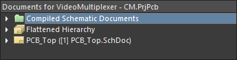
Individual Sheets ( ) ) |
캡처된 각 회로도 시트에 대해 아이콘을 표시하며, 한 번 클릭하면 Navigator 패널에 결과가 표시되고, 더블클릭하면 그래픽 편집 공간에도 결과가 표시됩니다. |
| Flattened Hierarchy (전체 프로젝트 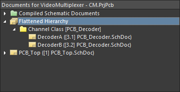 ) ) |
전체 프로젝트 전반의 모든 객체와 연결성을 표시합니다. 설계에 반복 시트(채널)가 있는 경우, 채널 이름(반복 시트의 한 번 클릭하면 Navigator 패널에 결과가 표시되고, 더블클릭하면 그래픽 편집 공간에도 결과가 표시됩니다. |
Full Design Hierarchy (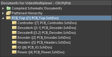 ) ) |
프로젝트의 모든 논리 시트에 대해 아이콘을 표시합니다. 설계에 반복 시트(채널)가 있는 경우, 한 번 클릭하면 Navigator 패널에 결과가 표시되고, 더블클릭하면 그래픽 편집 공간에도 결과가 표시됩니다. 반복 채널의 아이콘을 더블클릭하면 해당 채널의 시트를 표시하는 것과 함께, 회로도 편집 공간 하단에서 해당 특정 채널의 탭이 선택됩니다. |
 ).
).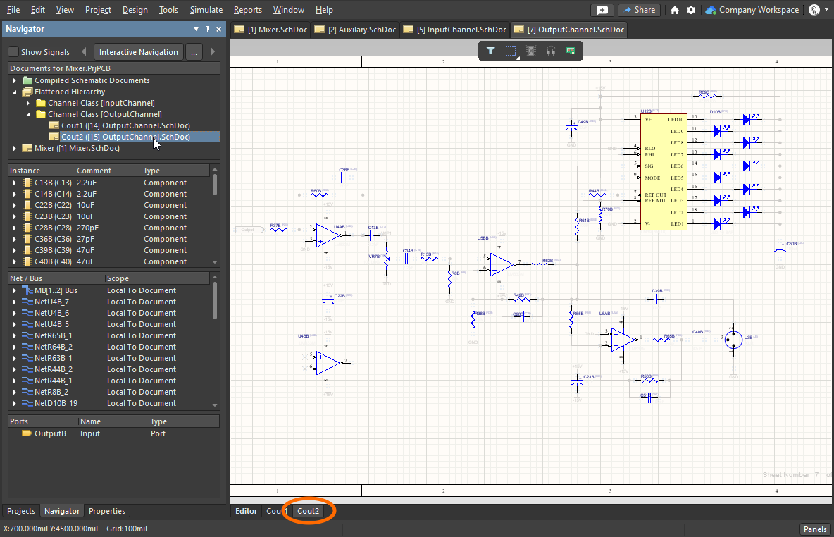 ).
).컴포넌트 섹션
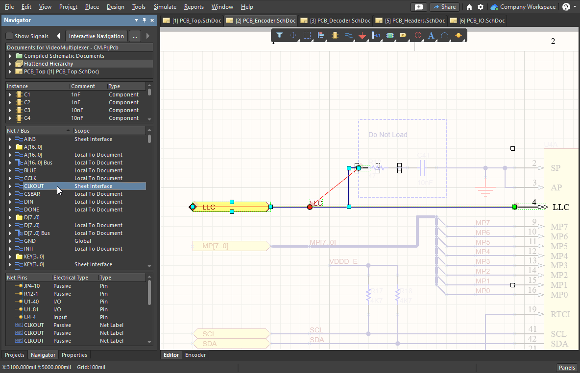
패널의 두 번째 영역에는 첫 번째 섹션에서 현재 선택된 문서에 존재하는 모든 컴포넌트가 포함됩니다. 목록에서 최상위 컴포넌트 인스턴스 항목을 선택하면 해당 항목을 기준으로 필터가 적용되며, 시각적 결과는 선택된 하이라이팅 방법에 따라 달라집니다. 활성화된 Highlighting 옵션 에 Connective Graph 옵션이 포함되어 있으면, 선택한 컴포넌트에 연결된 다른 모든 컴포넌트도 표시됩니다(필터가 확장되어 포함됨). 연결된 컴포넌트는 녹색 그래프 연결선으로 시각적으로 하이라이트됩니다.
 Connective Graph가 활성화되어 있으므로, 패널에서 선택한 컴포넌트에 연결된 각 컴포넌트까지 녹색 선이 그려집니다.
Features of the Components Section
컴포넌트 섹션 |
|
| Information available | 각 컴포넌트 항목에는 Parameters 및 Implementations (모델)용 하위 폴더가 있습니다. highlighting options에서 Pins 옵션이 활성화되어 있으면, Pins 하위 폴더도 사용할 수 있습니다(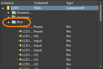 ). ). |
| When you click | Instance 목록에서 핀 항목을 클릭하면, 해당 핀에 대응하는 항목이 패널의 Net / Bus 섹션에서 선택 상태가 되며, 해당 상위 넷(parent net)의 모든 핀이 패널 하단 섹션에 나열됩니다. 또한 선택한 핀 항목을 기준으로 필터가 적용되며, 시각적 결과는 활성화된 하이라이팅 방법에 의해 결정됩니다. |
| Connective Graph | Connective Graph 옵션을 활성화한 경우, 선택한 핀의 상위 넷에 연결된 다른 모든 핀도 표시됩니다(필터가 확장되어 포함됨). 연결된 핀의 상위 넷은 빨간 그래프 연결선(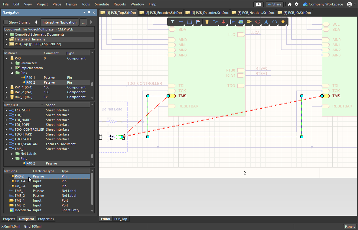 )으로 시각적으로 하이라이트됩니다. )으로 시각적으로 하이라이트됩니다. |
넷 / 버스 섹션
패널의 세 번째 섹션에는 탐색 중인 문서(또는 평탄화된 계층)의 각 넷과 버스가 나열됩니다. 항목을 클릭하면 넷/버스에 연관된 모든 객체(핀, 넷 라벨, 포트, 시트 엔트리, 크로스-시트 커넥터)가 활성화된 하이라이팅 방법에 따라 설계 편집기 창에 표시됩니다.
Features of the Net / Bus Section
넷 / 버스 섹션 |
|
| Information available | 선택된 넷/버스에 연관된 다양한 객체 유형은, 현재 활성화된 highlighting options 및 선택된 넷/버스에 해당 객체 종류가 존재하는지 여부에 따라 하위 폴더로 나뉘어 나열됩니다. 각 넷/버스에는 연관된 핀/포트/넷 라벨/시트 엔트리/크로스-시트 커넥터를 연결하는 데 사용된 그래픽 선을 나열하는 추가 하위 폴더가 포함될 수도 있습니다. 선 항목을 클릭하면 해당 선 객체만 필터링하고 시각적 제어 설정을 적용합니다. |
| When you click | 패널에서 표시하도록 활성화된 모든 넷 객체(그래픽 선 제외)는 패널 하단 섹션( )에 표시됩니다. 여기서도 항목을 클릭하면 활성화된 하이라이팅 방법에 따라 필터링이 적용됩니다. )에 표시됩니다. 여기서도 항목을 클릭하면 활성화된 하이라이팅 방법에 따라 필터링이 적용됩니다. |
버스 넷 - 넷 핀 섹션
패널의 네 번째 섹션 내용은 두 가지에 따라 달라집니다. 탐색 중인 객체와, 표시하도록 설정한 객체입니다. Net / Bus 섹션에서 bus를 클릭하면 해당 버스에 포함된 넷이 이 섹션에 나열됩니다. Net / Bus 섹션에서 net를 클릭하면 해당 넷의 핀이 나열됩니다. 또한 표시가 활성화되어 있다면, 해당 넷에 부착된 넷 식별자도 함께 나열됩니다.

신호 섹션
Navigator 패널은 일반적으로 제공하는 객체 중심 방식 대신, 신호 중심 방식으로 설계를 볼 수 있도록 지원합니다. 패널의 Documents 섹션에서 회로도 문서가 선택된 상태에서, 패널 상단의 Show Signals 옵션을 활성화하면 패널의 세 번째 섹션이 Signal 모드로 전환됩니다.
신호 항목을 클릭하면 필터가 적용되고, 해당 신호의 노드(핀/포트/넷 라벨/시트 엔트리/크로스-시트 커넥터)가 활성화된 하이라이팅 방법에 따라 설계 편집기 창에 표시됩니다. 목록의 각 신호에 대해, 그 신호와 연관된 노드 핀, 시트 엔트리 또는 크로스-시트 커넥터가 나열됩니다. 이러한 항목은 해당 객체 유형의 표시 옵션이 활성화되어 있는지 여부와 관계없이 표시됩니다.

Features of the Signal Section
신호 섹션 |
|
| Signal | 신호 이름(버스 또는 넷 이름). |
| Width | 이 신호 내의 개별(discrete) 넷 개수. |
| Click on a top-level signal entry | 최상위 신호 항목을 클릭하면, 해당 신호와 연관된 모든 신호 노드로 패널 하단 섹션이 채워집니다. 여기에는 핀, 넷 라벨, 포트, 시트 엔트리, 크로스-시트 커넥터가 포함될 수 있습니다. 항목은 해당 객체 유형을 표시하도록 하는 옵션이 활성화된 경우에만 표시됩니다. |
| Click on a sub-entry | 메인 Signal 목록에서 하위 항목을 클릭하면, 해당 신호의 상위 넷에 연관된 모든 넷 객체로 패널 하단 섹션이 채워집니다. |
| SignalName Driven By Pin X | 신호와 연관된 노드 핀이 출력 핀 또는 I/O 핀일 때 표시됩니다. X는 신호를 구동하는 컴포넌트-핀 지정자를 나타냅니다. |
| Driving Node Pin X | 신호와 연관된 노드 핀이 입력 핀일 때 표시됩니다. X는 신호에 의해 구동되는 컴포넌트-핀 지정자를 나타냅니다. |
| Driven By Node Sheet Entry SignalName | 시트 엔트리 노드의 전기적 타입이 출력 또는 I/O일 때 표시되며, 해당 엔트리가 신호를 구동합니다. |
| Driving Node Sheet Entry X | 시트 엔트리의 전기적 타입이 Input일 때 표시되며, 해당 엔트리는 신호에 의해 구동됩니다. |
PCB 탐색
Navigator 패널에서 클릭하여 회로도의 객체로 이동하는 것뿐 아니라, 동시에 PCB에서 해당 객체로도 이동할 수 있습니다. Navigator 패널에서 객체를 클릭할 때 Alt 키를 누르고 있으면, 대상 객체가 회로도와 PCB 양쪽에서 하이라이트됩니다.
탐색은 항상 회로도에서 발생하므로, PCB의 객체로 이동하려면 회로도와 PCB를 동시에 표시해야 합니다. PCB를 별도 창에 표시하거나, Split Vertical 또는 Split Horizonal 기능을 사용해 그래픽 공간을 공유(아래는 수직 분할 예시)하면 됩니다. 각 기능의 명령은 문서 탭을 우클릭했을 때 나타나는 컨텍스트 메뉴에서 사용할 수 있습니다.
디자인을 탐색할 때 Alt 키를 누른 채로 이동하면 PCB에서도 해당 객체를 함께 찾을 수 있습니다.
Altium Designer에는 회로도와 PCB 간 작업을 위한 다양한 기능이 포함되어 있으며, 예를 들면 다음과 같습니다.
| Cross probe | 크로스 프로브(Cross probe) - 마우스 오른쪽 버튼을 클릭해 실행한 다음, 한 편집기에서 객체(컴포넌트, 핀, 넷)를 클릭하면 다른 편집기에서 해당 객체로 이동합니다. 두 가지 모드가 있으며, continuous(소스 편집기에 머무름) 또는 jump-to(대상 편집기/문서를 활성 문서로 전환)입니다. 크로스 프로브 중에 Ctrl를 누르면 jump-to 모드가 호출됩니다. 크로스 프로브는 다음에서 지원됩니다: 회로도, PCB 및 BOM 편집기, Constraint Manager, 그리고 Project, Navigator, Messages 패널. |
| Cross select | 한 편집기에서 컴포넌트를 클릭해 선택하면 다른 편집기에서도 해당 컴포넌트가 선택되도록 합니다. 회로도 편집기와 PCB 편집기 간에 지원되며, View 메뉴에서 활성화합니다. |
Cross Probing and Cross Selection에 대해 자세히 알아보기
Navigator Panel 컨텍스트 메뉴

Navigator 패널의 마우스 오른쪽 버튼 컨텍스트 메뉴에는 다음 명령이 포함됩니다.
 AI로 번역됨