
PCB Libraries
The real-world component that gets mounted on the board is represented as a schematic symbol during design capture and as a PCB footprint for board design. Altium Designer components can be:
- Created in and placed from local libraries or
- Placed directly from a connected Workspace, accessible for the entire design team.
Footprints can be copied from the PCB editor into a PCB library, copied between PCB libraries, or created from scratch using the Footprint Wizard or drawing tools.
Creating a New PCB Library
To create a new PCB library, select the File » New » Library command from the main menus and select the PCB Library option from the File region of the New Library dialog.
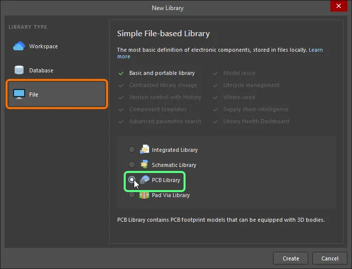
After clicking Create, a new PCB library document named PcbLib1.PcbLib is created and shown in the Projects panel, and an empty component sheet called PCBComponent_1 displays.
The content of the library is shown in the PCB Library panel.
You are now ready to add, remove, or edit the footprint components in the new PCB library using the PCB footprint editor commands.
Creating a PCB Library from a PCB Document
If you have a PCB design with all the footprints already placed, you could use the Design » Make PCB Library command in the PCB editor to generate a PCB library that includes only those footprints. This is very useful if you want to create an exact working library, or archive, of your finished design.
After launching the command, a library document (<PCBDocumentName>.PcbLib) will be automatically created (and stored in the same location as the PCB document from which it was created) and added to the project. The created file will appear in the Projects panel as part of the project, under the Libraries\PCB Library Documents sub-folder. The document will open as the active document in the PCB footprint editor. Each unique PCB component detected on the PCB will then be added to the library.
Creating a New PCB Footprint
Any number of PCB footprints can be created in a PCB library. To create a new PCB footprint in an existing library, select the Tools » New Blank Footprint command from the main menus, right-click in the design space then choose the Tools » New Blank Footprint command from the context menu, or right-clicking in the Footprints region of the PCB Library panel then choosing New Blank Footprint from the context menu.
Since a new library always contains one empty PCB footprint, you can also rename Component_1 to get started on creating a footprint. To do this, select PCBComponent_1 from the Footprints list in the panel then click the Edit button in the panel or double-click PCBComponent_1 to open the Footprint tab of the Properties panel in its Library Options mode. Type the new footprint name that uniquely identifies it in the Name field.
To remove the active footprint from the current PCB Library document, choose the Tools » Remove Footprint command from the main menus or right-click in the design space then choose the Tools » Remove Footprint command from the context menu. After launching the command, a confirmation dialog will appear asking whether you want to proceed with the deletion. After clicking Yes, the footprint will be removed from the library document and the previous footprint in the Footprints list will be made active. One or more library footprints can also be deleted directly in the PCB Library panel. Select the required footprint(s) in the Footprints list, right-click then choose the Delete command from the context menu. A confirmation dialog will appear asking whether you want to proceed with the deletion of n footprints. After clicking Yes, the footprint(s) will be removed from the library document and the subsequent footprint in the Footprints list will be made active.
Creating a Footprint Using the IPC Footprint Batch Generator
In addition to the techniques described on the Creating a PCB Footprint page, the IPC Footprint Batch Generator can be used to generate multiple footprints at multiple density levels. The generator reads the dimensional data of electronic components from an Excel spreadsheet or comma-delimited file then applies the IPC equations to build PCB footprints that are truly compliant with Revision B of the IPC standard 7351 - Generic Requirements for Surface Mount Design and Land Pattern Standard.
The batch generator can create the following footprint types: BGA, BQFP, CAPAE, CFP, CHIP, Chip Array, CQFP, DFN, DIP, DPAK, FM, LCC, LGA, MELF DIODE/RESISTOR, MOLDED CAP/IND/DIODE, PLCC, PQFN, PQFP, PSON, QFN, QFN-2ROW, SIP, SODFL, SOIC, SOJ, SON, SOP, SOT143/343, SOT223, SOT23, SOT89, SOTFL, WIRE WOUND, and ZIP.
Support for the IPC Footprints Batch Generator includes:
-
Package type blank template files are included in the
\Templatesfolder in the Altium Designer installation. - Package input files can contain the information for one or more footprints of a single package type and can be either an Excel or comma-delimited (CSV) format file.
Select the Tools » IPC Compliant Footprints Batch Generator command from the main menus to access the IPC Compliant Footprints Batch Generator dialog. Use the dialog to add the footprint package files that you need to process, and set generation options as required.

The IPC Footprints Batch Generator has options to either create all the footprints in the open PCB footprint library or generate a single library based on either an input file or footprint name.
The process is summarized as follows:
- Add files to be processed to the list. These can be Excel-based, or CSV-based. Use the Add Files/Remove Files buttons to craft the list, or simply drag and drop files into the list area.
- Specify an output folder for generated output (if generating new PCB Library files as part of the process).
- Use the options to determine how the footprints are generated. All footprints can be generated in the active PCB Library document. Alternatively, generate one PCB Library document per input file (named the same as the input file), or one PCB Library document per footprint name (named using the FootprintName field specified in the file, or using IPC naming if this is blank). Generated library files will be stored in accordance with the nominated Output Folder.
- Optionally, choose to have a HTML-based report created (and optionally opened after processing completes). This lists the date, time, and processing time, along with all the files processed, and any related fatal errors, errors, and warnings.
- If you have opted to generate new PCB libraries, you can also opt to have these opened after generation is complete.
After defining the list of files to be processed and all other options as required, click Start. Processing will proceed, with progress reflected in the dialog. You can cancel at any time by clicking Stop, or Close. Once the generation of all footprints has finished, click Close to leave the dialog, and enjoy the fruits of the generator's labor.
Options and Controls of the IPC Footprints Batch Generator Dialog
- Text Box - a list of files to be processed.
-
Open Template - click to open the Open Template dialog then choose a template type from the drop-down. Click OK to open the underlying Excel template for the current data sets.
- Help On - click to open the Help On dialog then choose the template type to access reference information or use the drop-down to select the desired package type.
- Add Files - click to select package input files to add input package type files to the text box.
- Remove Files - click to remove the selected file(s) in the text box.
- Output Folder - use the browse button to search for and set the desired output location.
-
Produce STEP model - enable to generate a STEP model.
- Model Folder - use the browse button to search for and choose the location of the desired model.
- Generate all footprints in - enable to generate all footprints in the current PCB Library.
- Generate single PcbLib files per input file - check to generate a PCB Library file in the output folder with the same name as the input file being processed. The footprints from this file will be added to the PCB Library.
- Generate single PcbLib files per footprint name - check to generate a PCB Library file in the output folder for every package in the input files.
-
Generate report on completion - check to generate a report upon completion.
-
Open generated report - check to open the generated report. This option is only available if Generate report on completion is checked.
-
- Open generated PcbLib files on completion - check to open the generated PCB Library files upon completion. This option is only accessible if Generate single PcbLib files per input file is checked.
- Processing - an incremental bar that shows the progress of the batch generation process.
- Start/Stop - click Start to launch the batch generation. Once the Start button is used, it then changes to Stop; click Stop to stop the batch process.
- Close - click to stop the batch process and close the dialog.
Adding Footprints from Other Sources
PCB components can be copied from other PCB libraries and then renamed and modified within the destination library to match the specifications required. There are a number of ways to execute this function.
- Select placed footprint(s) in a PCB document then copy (Edit » Copy) and paste them into an open PCB library using Edit » Paste Component. If multiple components have been copied to the clipboard from the PCB editor, all will be pasted into the library document as separate component footprints.
- Select Edit » Copy Component when the footprint to be copied is active in the PCB Library Editor, change to the open PCB destination library then select Edit » Paste Component.
-
Select one or more footprints in the list in the PCB Library panel using the standard Shift+Click or Ctrl+Click, right-click then choose Copy. Switch to the target library, right-click in the list of footprint names then choose Paste
nComponents, wherenis the number of components.
Note that if the component was placed on the PCB from your connected Workspace or from the Manufacturer Part Search panel, a link to the source Workspace remains. You can clear the Workspace links for all components within the open library by choosing the Tools » Clear Server Links command from the main menus. After launching the command, the Confirm Clear Vault Links dialog opens. Click Yes to clear the Workspace links specified in the dialog and save the library; click No to exit from the dialog with no action.
Checking the Footprints and Generating Reports
To check that the new footprints have been created correctly, there are several reports that can be generated.
Library List
To generate a report listing all PCB footprints in the current PCB Library document, choose the Reports » Library List command from the main menus. After launching the command, the report will be generated (<PCBLibraryDocumentName>.REP) in the same folder as the source PCB Library document and will automatically be opened as the active document in the main design window. The report summarizes the total number of component models in the library and lists all of the component models by name.
The report will be added to the Projects panel as a free document under the Documentation\Text Documents sub-folder.
Library Report
You can generate a report from the active library document, containing information about the components stored within that library. The report can be configured to include component previews (drawn in color or left black and white). The report can be generated as a Microsoft Word document (*.doc), or as a standard HTML document (*.html).
Select the Reports » Library Report command from the main menus to open the Library Report Settings dialog. Use this dialog to configure the content and style of the report, and also where (and by what name) the report is to be generated. By default, the report will be named after the PCB library, and stored in the same location.

The Library Report Settings dialog
Options and Controls of the Library Report Settings Dialog
Output File Name
- Output File Name - displays the entire output file including path. Use the browse folder icon to search for and select a different location and name
- Document style - the file extension will be .doc and a word document format will be generated for the library report.
- Browser style - the file extension will be .html and a web page will be generated in an internet browser. You can edit the full output file name if desired.
- Open generated report - enable to open the generated report either in MS Word or an internet browser.
- Add generated report to current project - enable to add the generated report to the current project.
Draw Components' previews
Enable to draw a preview for components in the report.
Settings
- Use Color - enable to allow the library report to contain elements in color for either word or web documents.
After clicking OK the report will be generated. If you have opted to have the report opened after generation, this will happen provided you have either Microsoft Word (if generating a Doc style report), or Microsoft Internet Explorer (if generating a HTML style report) installed on your computer.
If you have chosen to add the generated report to the project after generation, it will appear in the Projects panel under the Generated\Documents sub-folder (for a HTML style report), or the Generated\Text Documents sub-folder (for a Doc style report).
Component Rule Checker
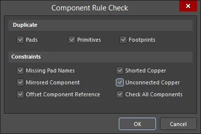
To validate all components in the active library, the PCB footprint editor provides a Component Rule Checking feature. This feature offers a number of checks, including checking for duplicate primitives, missing pad designators, floating copper and an inappropriate component reference. The result is a text-based report that lists any violations of these checks. To run the Component Rule Check:
- Save your library file.
-
Select Reports » Component Rule Check (shortcut R, R) to open the Component Rule Check dialog.
-
Check all the boxes available then click OK. A report titled
<LibraryName>.ERRis generated and opens in the Text Editor. Any errors will be noted. Each component footprint that is found to be in error is listed, along with the specific tests that it failed. - Close the report to return to the PCB footprint editor.
Updating a PCB Footprint
Updating a PCB Footprint from a PCB Library can be done in two ways: "Pushing" the PCB from the PCB Library, or by "Pulling" from the PCB editor. Pushing a PCB Footprint update takes a selected footprint(s) from the PCB Library and uses it to update all open PCB documents containing that footprint. This first method is the best option when a complete replacement is desired. The second option allows you to review all the differences between the existing footprint and the footprint in the library before the update is performed. You can also select which objects are to be updated from the library. This second method is the best option when you need to figure out exactly what has changed between the footprint on the board and the footprint in the library.
Pushing Footprint Updates from the PCB Library
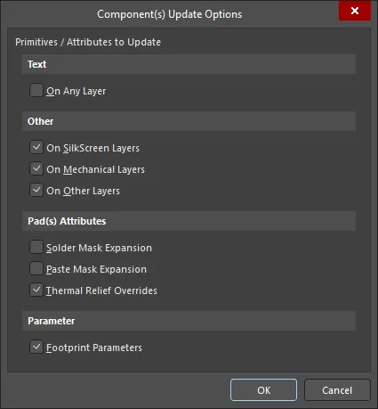
From the PCBLIB Editor, use the Tools » Update PCB with Current Footprint (when the footprint whose changes you want to pass to the PCB document(s) is the active footprint) or Tools » Update PCB With All Footprints command. From the PCB Library panel, right-click in the Components region of the PCB Library panel then select Update PCB with [Component] or Update PCB with All. Running these commands opens the Component(s) Update Options dialog from where you can select the primitives/attributes to be updated. Use this dialog to determine which aspects of the footprint are to be updated. After clicking OK, all placed instances of this footprint on all open PCB documents will be updated with any changes made in accordance with specified update options.
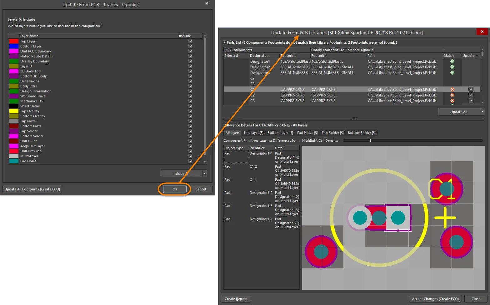
Pulling Footprint Updates from the PCB Editor
From the PCB editor, use the Tools » Update From PCB Libraries command, which, in turn, opens the Update From PCB Libraries - Options. Click OK to open the Update From PCB Libraries dialog.
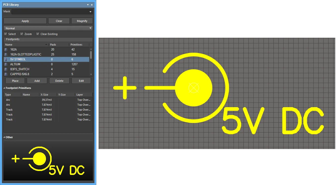
PCB Library Panel
The PCB Library panel enables you to browse footprints stored in the active PCB library document and edit their properties. When a PCB Library document is active, the panel becomes populated with information pertaining to the constituent footprints of that library. The panel also offers the ability to pass on any changes made to them directly to the PCB design document.

The PCB Library panel
PCB Library Panel Content and Use
Library Browsing
The panel has three main sections, each offering a different scope or view of the footprints in the active PCB Library:
- Footprints - a list of footprints in the active library. The number of pads and primitive objects used to define the footprint is listed for each entry.
- Footprint Primitives - the primitive objects and their main properties that make up the currently selected footprint.
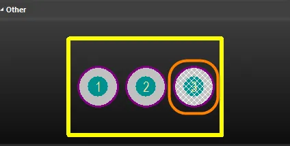
- Other - a simplified, overall view of the currently selected footprint with the main editor view indicated by an overlay graphic.
As a footprint is selected in the panel, its constituent primitives populate the Footprint Primitives section and the footprint is displayed in the main editor design space. Selecting a primitive object in the panel causes the corresponding object to be highlighted in the editor design space. In this way, the PCB Library panel offers a fast and easy way to browse, view and access PCB library footprints.
Filtering Content
The contents of the list can be filtered, enabling you to quickly find a particular footprint within the library. This is especially useful if the library contains a large number of items. Filtering can be applied using the following methods:
Indirect Filtering
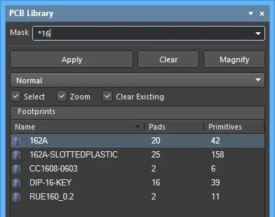
This method uses the Mask field at the top of the panel to filter the contents of the list. Masking is applied based on the entry in the field. Only those footprints in the list targeted by the scope of the entry will remain displayed.
Use the * wild card operator for more elaborate filtering. For example, typing m* will display only footprints whose names begin with m, or as in the image below, typing *16 will display only footprints that contains 16 in the name.
Direct Filtering
This method is available for all list regions in the panel and allows you to quickly jump to an entry by directly typing within the area of the list. Masking is not applied, leaving the full content of the list visible at all times.
To use the feature to quickly find a footprint, click inside the Footprints section of the panel then type the first letter of the footprint to which you want to jumps. For example, if you wanted to quickly jump to footprint entries starting with the letter S, you would press "S" on the keyboard. The first footprint in the list starting with S will be made active, and the letter will be highlighted to indicate that filtering of the list is based upon it.
If there are multiple footprints starting with the same letter and especially if the library is particularly large, type additional letters to target the specific entry you require, for example, "SO" as shown below.

Combination Filtering
In some situations, it may be helpful to use Indirect and Direct filtering together. If, for example, you recall that the footprint you want to locate has a sub-type number of 4 and a prefix of PO, this information can be used as Indirect (Mask) and Direct entries.
Footprints Controls
- Place - click to place the selected footprint.
-
Add - click to add a new footprint to the list. The default name will be
PCBCOMPONENT_1. - Delete - click to delete the selected footprint. A dialog will open asking for confirmation before the delete occurs.
- Edit - click to open the Properties panel to edit the properties of the selected footprint.
Browsing Footprint Primitives
The Footprint Primitives section lists all primitive objects that constitute the footprint currently selected in the Footprints list. For each primitive entry, the following information is displayed:
- Type - the type of primitive object (e.g., pad, track, arc, etc.).
- Name - the specified value for the objects' designator (where one exists).
- X-Size - the X dimension of the object (e.g., the width of an arc, track or fill, the X-Size value of a pad).
- Y-Size - the Y dimension of the object (e.g., the height of a fill, the Y-Size value of a pad). This field will be empty for a track or arc.
- Layer - the layer upon which the object resides.
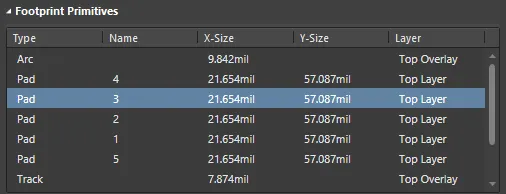
As individual object primitives are selected in the panel, the matching object (track, arc, pad, etc.,) is graphically highlighted in the editor design space.
Controlling the Display of Browsed Entries in the Design Space
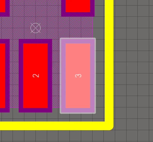
Selecting an entry in either panel list region applies a filter, essentially using the entry as its scope. The visual result of the applied filtering on the document in the design editor window is determined by a series of highlighting controls located at the top of the panel.
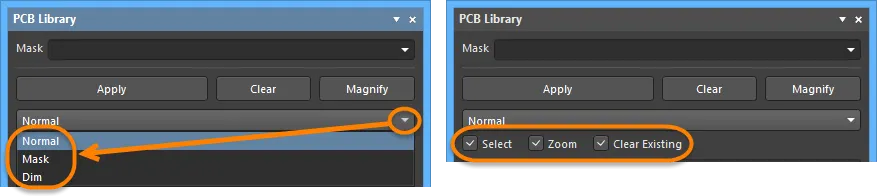
-
Mask / Dim / Normal - provides the options for visibly contrasting filtered and unfiltered objects within the design editor window. The effectiveness of masking and dimming is determined by the Highlighting Options set in the PCB Editor - Display page of the Preferences dialog.
- When Mask is selected, filtered objects will appear visible in the design editor window, with all other objects being made monochrome. When this option is applied, unfiltered objects will be unavailable for selection or editing.
- When Dim is selected, filtered objects will appear visible in the design editor window, with all other objects retaining their colors but shaded.
- Select - when enabled (default), the filtered objects will be selected in the design space.
- Zoom - when enabled (default), the filtered objects will be zoomed and centered (where possible) in the design space.
- Clear Existing - when enabled (default), an existing filter will be cleared before applying a new one. Disabling this option allows you to extend an existing filter, essentially refining the filter further by applying a new filter in addition to the existing one.
Any combination of these options can be enabled. For example, you might want to have all filtered objects zoomed, centered and selected in the design space as well as applying masking to take away the clutter of other design objects. Use the Clear button to clear the currently-applied filter. All objects in the design space will become fully visible and available for selection/editing. If you want to re-apply the filter, click the Apply button.
Using the Panel's Mini-viewer
The bottom section provides a mini-viewer for the document, with an image of the active footprint central to its window. The area currently displayed in the design editor window is denoted by white hash marks as highlighted in the following image.
Click the Magnify button at the top of the panel to provide a floating magnifying glass and zoom cursor in the design editor window. As you move these around in the design space, the mini-viewer in the panel will contain the magnified image of the active footprint centered on the cursor. This allows you to browse the document at full size in the design editor window, while looking at zoomed detail in the mini-viewer window.
Use the Page Up and Page Down keys to increase or decrease the magnification. Right-click, click or press Esc to exit magnify mode.
Right-click Menus
Footprints
- New Blank Footprint - select to add a new footprint to the list. The footprint is given the default name PCBCOMPONENT_1 and a blank sheet is opened in the design editor window, ready for you to start placing the primitive objects that will define it.
- Footprint Wizard - click to open the Footprint Wizard. The pages of the Wizard will guide you through the steps to creating a new component footprint.
- Cut - place a copy of the selected footprint(s) onto the PCB Library Editor's internal clipboard then permanently delete the footprint(s) from the library. A confirmation dialog will appear asking for verification to proceed with the deletion.
- Copy - place a copy of the selected footprint(s) onto the PCB Library Editor's internal clipboard.
- Copy Name - copy the name of the focused footprint to the PCB Library Editor's internal clipboard.
- Paste - paste a footprint from the PCB Library Editor's internal clipboard into the active library document. The entry for this command will change to reflect how many valid footprints are on the clipboard.
- Delete - permanently delete the selected footprint(s) from the library document. A confirmation dialog will appear asking for verification of whether or not to proceed with the deletion.
- Select All - quickly select all footprint entries in the list.
- Footprint Properties - click to access the Properties panel to view/modify the Name, Description, Type, Height, Area, and Parameters for the focused footprint. The Properties panel for the footprint will also open when a footprint entry is double-clicked in the panel.
- Place - place the focused footprint onto the PCB design document. When clicked, the last PCB to have been active (regardless of the project to which it belongs) will be made the active document in the design space.
- Update PCB With <FocusedFootprint> - pass on changes made to the focused footprint within the library document to all open PCB design documents where that footprint has been placed. All instances of the footprint will be updated.
- Update PCB With All - pass on all changes made to footprints within the library document to all open PCB design documents where these footprints have been placed. All placed instances of a changed footprint will be updated.
-
Report - generate a report for the active footprint. After launching the command, the report will be generated (
LibraryName.CMP) in the same folder as the source PCB library document and will automatically be opened as the active document in the design editor window. The report lists information including footprint dimensions, a breakdown of the primitive objects that constitute the footprint, and the layers on which they reside. - Delete All Grids And Guides In Library - click to delete grids and guides for this library.
Footprint Primitives
-
Show Pads - enable to display pad entries.
-
Show Vias - enable to display via entries.
-
Show Tracks - enable to display track entries.
-
Show Arcs - enable to display arc entries.
-
Show Regions - enable to display region entries.
-
Show Component Bodies - enable to display component body entries.
-
Show Fills - enable to display fill entries.
-
Show Strings All - enable to display string entries.
-
Show Bond Wires - enable to display bond wire entries.
- Select All - quickly select all footprint primitive entries in the list.
- Report - generate a primitive information report for the focused footprint in the Footprints section of the panel. After launching the command, the Report Preview dialog will open containing the primitive information currently displayed in the Footprint Primitives region of the panel. Use the dialog to view, print and export the report in various file formats.
- Properties - access the corresponding Properties panel for the focused primitive in which you can view and modify properties as required. The primitive's corresponding Properties panel also will open when a primitive entry is double-clicked in the panel.
Notes
- Standard Ctrl+Click and Shift+Click functionality is supported for selection of multiple entries in a list.
- The active footprint is that whose graphics are currently displayed in the design editor window. A footprint can be active without necessarily being selected and/or focused in the Footprints list.
- Ctrl+Click over a selected entry in a list to deselect it. If the entry is the only one selected for that section, performing this action will clear the filter.
- The keyboard shortcuts Home, Down Arrow, Up Arrow, and End and the First Component, Next Component, Previous Component, and Last Component commands from the design space's Tools right-click sub-menu can be used to display the first, next, previous, and last footprint, respectively.
- In regions of the panel where multiple columns of data exist, the data may be sorted by any column by clicking on the header for that column. Clicking once will sort in ascending order; click again to sort by descending order.
- You can change the order in which columns of data are displayed. To move a column, click on its header and drag it horizontally to the required position. A valid position is indicated by the appearance of two positional arrows.
- The filtering applied when browsing design objects is permanent. If the Mask or Dim highlight method has been selected, all objects not falling under the scope of the filter will become faded (depending on settings) in the design space and are not available for selection or editing. Clicking inside the design editor window will not clear the filter. A permanent filter must be cleared by clicking on the Clear button from within the panel.
- The footprint that you paste into the active library document can originate from either a PCB design document or another PCB library document.
- If multiple footprints have been copied to the clipboard from the main design in the PCB Editor, only the last footprint of the group to have been selected will be pasted into the library document.
- If the same footprint is pasted into the library more than once or if more than one new footprint is added to the library without renaming, the copies are distinguished by the suffix - DUPLICATE, - DUPLICATE1, - DUPLICATE2, etc.
- A PCB design document must be open before a library footprint can be placed using the Place command.
- A PCB design document must be open in order to pass on changes made to footprints in the library document.
-
When a new PCB library document is created the panel will, by default, contain a single, blank footprint -
PCBCOMPONENT_1. -
Library footprints can be edited only in the source PCB library (
*.PcbLib). You cannot edit the footprints in an integrated library (*.IntLib). You would have to de-compile the integrated library first then edit the required footprint(s) in the source PCB library document(s). The source can then be recompiled to produce the updated integrated library.