
Panel nawigacyjny

Altium Essentials: Navigating Schematics
This content is part of the official Altium Professional Training Program. For full courses, materials and certification, visit Altium Training.
Jeśli projekt jest duży i rozłożony na wiele arkuszy, śledzenie sieci (net) i weryfikacja połączeń w projekcie wyłącznie na podstawie schematów może stać się trudne. Odnalezienie tych samych obiektów na PCB stanowi jeszcze większe wyzwanie. Aby ułatwić ten proces, używa się panelu Navigator .

Używaj panelu Navigator jako „okna” na cały projekt. Przytrzymaj Alt podczas klikania w panelu, aby dodatkowo zlokalizować ten element na PCB.
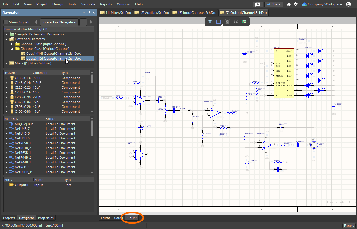
Panel Navigator umożliwia przeglądanie albo aktywnego źródłowego dokumentu schematu, albo wszystkich źródłowych dokumentów schematu w aktywnym projekcie. Panel wykorzystuje jako podstawę nawigacji model połączeń projektu, który jest automatycznie tworzony w tle. Panelu można też używać do nawigacji do komponentów, padów, magistral i sieci na PCB.
Nawigacja po projekcie
Nawigację można wykonywać na dwa sposoby – albo klikając w panelu Navigator, aby zlokalizować obiekt na schemacie, albo klikając obiekt na schemacie, aby zlokalizować go w panelu Navigator.
 )
)Z panelu Navigator
Aby wyświetlić panel Navigator, użyj przycisku Panels w prawym dolnym rogu programu lub wybierz View » Panels » Navigator z menu.
Informacje o komponentach i połączeniach zostaną załadowane do panelu natychmiast po otwarciu schematu; kliknij ikonę w sekcji Documents, aby je wyświetlić. Oprogramowanie automatycznie buduje Dynamic Data Model dla całego projektu i utrzymuje ten model w miarę wykonywania operacji edycji. Zwróć uwagę, że karty dokumentów nie są wyświetlane (u góry graficznego obszaru edycji) dla wszystkich arkuszy schematu (są otwierane w tle) — karta pojawia się dopiero wtedy, gdy użytkownik wykona działanie na danym arkuszu.
Dynamic Data Model jest dostępny dla każdego z edytorów, a także dla panelu Navigator. Jeśli w dowolnym momencie nie masz pewności, czy zawartość panelu odpowiada bieżącemu stanowi projektu, wybierz polecenie Validate Project, aby wymusić odświeżenie modelu (menu Project lub menu kontekstowe po kliknięciu prawym przyciskiem w panelu Navigator).

Kliknij obiekt w panelu Navigator, aby zlokalizować wszystkie wystąpienia tego obiektu w całym projekcie.
Nawigacja interaktywna
Oprócz nawigowania z list obiektów prezentowanych w panelu i klikania, aby zlokalizować obiekt w przestrzeni graficznej, możesz też nawigować z przestrzeni graficznej z powrotem do listy. Ten tryb, nazywany nawigacją interaktywną, uruchamiasz, klikając przycisk Interactive Navigation u góry panelu Navigator. Kursor zmienia się w krzyżyk, co wskazuje, że jesteś w trybie nawigacji; pozostaje w nim do momentu kliknięcia prawym przyciskiem myszy lub naciśnięcia klawisza Esc .
Podczas nawigowania po projekcie wyświetlany arkusz będzie się aktualizował zgodnie z bieżącymi opcjami podświetlania, a panel Navigator będzie się aktualizował, aby pokazać informacje związane z aktualnym wyborem w graficznym oknie edycji.
, a następnie kliknij obiekt na arkuszu, aby zlokalizować go w panelu i w pozostałej części projektu.")
Wywołaj nawigację interaktywną (przycisk u góry panelu Navigator), a następnie kliknij obiekt na arkuszu, aby zlokalizować go w panelu i w pozostałej części projektu.
Skrót nawigacji interaktywnej
Oprócz uruchamiania nawigacji interaktywnej z panelu Navigator możesz wywołać nawigację w dowolnym momencie w edytorze schematu: przytrzymaj Alt i kliknij obiekt projektu. Możesz kliknąć dowolny obiekt, w tym przewód, etykietę sieci, port, wpis arkusza, symbol arkusza lub komponent.
Użyj skrótu Alt+Click, aby nawigować po projekcie.
Jak obiekty są podświetlane podczas nawigacji
Gdy klikniesz obiekt w panelu Navigator, obiekt jest wyświetlany w graficznym obszarze edycji. Sposób prezentacji obiektu zależy od ustawień System - Navigation w oknie dialogowym Preferences. Aby uzyskać dostęp do ustawień bezpośrednio z panelu Navigator, kliknij przycisk Navigation Options (![]() ) u góry panelu, aby otworzyć okno dialogowe.
) u góry panelu, aby otworzyć okno dialogowe.
Obszar Highlight Methods okna dialogowego Preferences udostępnia opcje sterujące efektem wizualnym tymczasowego filtrowania, które jest stosowane do dokumentu podczas nawigacji — zarówno z panelu, jak i z poziomu samego dokumentu. Można włączyć dowolną kombinację tych opcji. Na przykład możesz chcieć, aby wszystkie filtrowane obiekty były powiększane i zaznaczane w oknie edytora projektu, jednocześnie stosując przyciemnianie, aby ograniczyć „szum” pozostałych obiektów projektu.
Navigation Highlight Methods
Metody podświetlania ( |
|
| Selecting | Gdy ta opcja jest włączona, filtrowane obiekty zostaną zaznaczone w obszarze roboczym. |
| Connective Graph | Włącz tę opcję, aby wyświetlić relacje połączeń między obiektami w aktywnym dokumencie w oknie edytora projektu.
|
| Zooming | Gdy ta opcja jest włączona, filtrowane obiekty zostaną powiększone i wyśrodkowane (o ile to możliwe) w oknie edytora projektu. Poziom powiększenia (tj. zakres powiększenia stosowany podczas nawigacji z panelu lub interaktywnie w dokumencie projektu) jest kontrolowany suwakiem Far / Close. Większe powiększenie uzyskasz, przesuwając suwak w prawo. |
| Dimming | Gdy ta opcja jest włączona, filtrowane obiekty będą w pełni widoczne w oknie edytora projektu, a wszystkie pozostałe obiekty zostaną przyciemnione. Kontrast między obiektami filtrowanymi a maskowanymi jest kontrolowany suwakiem None / Invisible. Silniejsze przyciemnienie uzyskasz, przesuwając suwak w prawo. |
 )
) ).
).Panel Navigator
Panel Navigator zapewnia wgląd w model połączeń projektu. Struktura projektu jest przedstawiona w czterech sekcjach panelu; każda sekcja została opisana poniżej.
 Panel Navigator przedstawia widok całego projektu zorientowany na połączenia.
Sekcja Documents
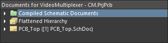
Umieszczona u góry panelu sekcja Documents udostępnia trzy różne sposoby przeglądania projektu – individual sheets, flattened hierarchy (cały projekt) lub możliwość przeglądania full design hierarchy. Kliknij ikonę w tej pierwszej sekcji jednokrotnie, aby wczytać dane do panelu; kliknij dwukrotnie, aby dodatkowo wyświetlić wyniki w graficznej przestrzeni edycji.
Features of the Documents Section
Sekcja dokumentów |
|
Individual Sheets ( ) ) |
Wyświetla ikonę dla każdego przechwyconego arkusza schematu, zidentyfikowanego przez Kliknij jednokrotnie, aby wyświetlić wyniki w panelu Navigator; kliknij dwukrotnie, aby dodatkowo wyświetlić wyniki w graficznej przestrzeni edycji. |
| Flattened Hierarchy (cały projekt 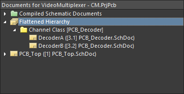 ) ) |
Wyświetla wszystkie obiekty i połączenia w całym projekcie. Jeśli w projekcie występują arkusze powtarzane (kanały), dla każdej klasy kanałów zostanie wyświetlona ikona podrzędna, identyfikowana nazwą kanału (pochodzącą z Kliknij jednokrotnie, aby wyświetlić wyniki w panelu Navigator; kliknij dwukrotnie, aby dodatkowo wyświetlić wyniki w graficznej przestrzeni edycji. |
Full Design Hierarchy (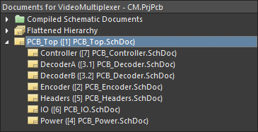 ) ) |
Wyświetla ikonę dla każdego arkusza logicznego w projekcie. Jeśli w projekcie występują arkusze powtarzane (kanały), istnieje ikona arkusza dla każdego kanału, identyfikowana przez Kliknij jednokrotnie, aby wyświetlić wyniki w panelu Navigator; kliknij dwukrotnie, aby dodatkowo wyświetlić wyniki w graficznej przestrzeni edycji. Jeśli dwukrotnie klikniesz ikonę powtarzanego kanału, oprócz wyświetlenia arkusza dla tego kanału zostanie wybrana karta dla konkretnego kanału na dole przestrzeni edycji schematu. |
 ).
). ).
).Sekcja komponentów
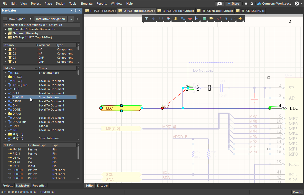
Drugi obszar w panelu zawiera wszystkie komponenty istniejące w dokumencie aktualnie wybranym w pierwszej sekcji. Gdy wybierzesz na liście wpis instancji komponentu najwyższego poziomu, zostanie zastosowany filtr na podstawie tego wpisu, a efekt wizualny zależy od wybranych metod podświetlania. Jeśli włączone opcje podświetlania obejmują opcję Connective Graph, widoczne będą także wszystkie pozostałe komponenty połączone z wybranym komponentem (filtr zostanie rozszerzony, aby je uwzględnić). Połączone komponenty są wizualnie wyróżniane zielonymi liniami połączeń grafu.
 Ponieważ włączony jest graf połączeń, do każdego komponentu połączonego z komponentem wybranym w panelu rysowana jest zielona linia.
Features of the Components Section
Sekcja komponentów |
|
| Information available | Dla każdego wpisu komponentu dostępne są podfoldery dla Parameters oraz Implementations (modeli). Jeśli w opcjach podświetlania włączona jest opcja Pins , dostępny będzie również podfolder Pins (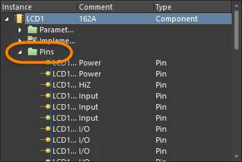 ). ). |
| When you click | Gdy klikniesz wpis pinu na liście Instance, odpowiadający mu wpis dla tego pinu zostanie zaznaczony w sekcji Net / Bus panelu, a wszystkie piny dla tej nadrzędnej sieci zostaną wyświetlone w dolnej sekcji panelu. Zostanie również zastosowany filtr na podstawie wybranego wpisu pinu; efekt wizualny zależy od włączonych metod podświetlania. |
| Connective Graph | Jeśli włączono opcję Connective Graph, widoczne będą także wszystkie pozostałe piny połączone z nadrzędną siecią wybranego pinu (filtr zostanie rozszerzony, aby je uwzględnić). Nadrzędna sieć dla połączonych pinów jest wizualnie wyróżniana czerwonymi liniami połączeń grafu (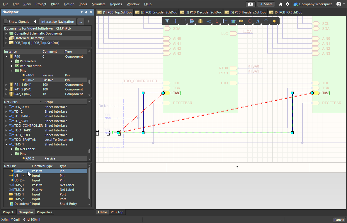 ). ). |
Sekcja Net / Bus
Trzecia sekcja panelu wyświetla listę wszystkich sieci i magistral w przeglądanym dokumencie (lub w spłaszczonej hierarchii). Po kliknięciu wpisu wszystkie obiekty powiązane z daną siecią/magistralą – piny, etykiety sieci, porty, wpisy arkusza oraz łączniki międzyarkuszowe – zostaną wyświetlone w oknie edytora projektu zgodnie z włączonymi metodami podświetlania.
Features of the Net / Bus Section
Sekcja Net / Bus |
|
| Information available | Różne typy obiektów powiązanych z wybraną siecią/magistralą są wymienione w podfolderach, zależnie od aktualnie włączonych opcji podświetlania oraz obecności danego typu obiektu w aktualnie wybranej sieci/magistrali. Dla każdej sieci/magistrali może zostać dołączony dodatkowy podfolder zawierający graficzne linie użyte do łączenia powiązanych pinów/portów/etykiet sieci/wpisów arkusza/łączników międzyarkuszowych. Kliknij wpis linii, aby przefiltrować tylko ten obiekt linii i zastosować ustawienia sterowania wizualnego. |
| When you click | Wszystkie obiekty sieci, które zostały włączone do wyświetlania w panelu (z wyjątkiem linii graficznych), będą pokazane w dolnej sekcji panelu (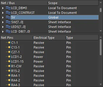 ). Ponownie, kliknięcie któregokolwiek z nich zastosuje filtrowanie zgodnie z włączonymi metodami podświetlania. ). Ponownie, kliknięcie któregokolwiek z nich zastosuje filtrowanie zgodnie z włączonymi metodami podświetlania. |
Magistrale – sekcja pinów sieciZawartość czwartej sekcji panelu zależy od dwóch rzeczy: obiektu, po którym nawigujesz, oraz obiektów ustawionych do wyświetlania. Jeśli klikniesz bus w sekcji Net / Bus, w tej sekcji panelu zostaną wyświetlone sieci należące do tej magistrali. Jeśli klikniesz net w sekcji Net / Bus, zostaną wyświetlone piny w tej sieci. Identyfikatory sieci dołączone do tej sieci również zostaną wyświetlone, jeśli są włączone do wyświetlania.

Sekcja sygnałów
Panel Navigator umożliwia przeglądanie projektu w ujęciu zorientowanym na sygnały, zamiast podejścia zorientowanego na obiekty, które standardowo prezentuje projekt. Jeśli w sekcji Documents panelu wybrano dokument schematu, włączenie opcji Show Signals u góry panelu przełącza trzecią sekcję panelu w tryb Signal.
Kliknij wpis sygnału, aby zastosować filtr; węzły dla tego sygnału (piny/porty/etykiety sieci/wpisy arkusza/łączniki międzyarkuszowe) zostaną wyświetlone w oknie edytora projektu zgodnie z włączonymi metodami podświetlania. Dla każdego sygnału na liście zostaną wymienione piny węzłów, wpisy arkusza lub łączniki międzyarkuszowe powiązane z tym sygnałem. Te wpisy będą wyświetlane niezależnie od tego, czy odpowiadająca im opcja wyświetlania dla danego typu obiektu jest włączona, czy nie.

Features of the Signal Section
Sekcja sygnałów
Signal
Nazwa sygnału (nazwa magistrali lub sieci).
Width
Liczba rozłącznych sieci w obrębie tego sygnału.
Click on a top-level signal entry
Kliknij wpis sygnału najwyższego poziomu, aby wypełnić dolną sekcję panelu wszystkimi węzłami sygnału powiązanymi z tym sygnałem. Mogą to być piny, etykiety sieci, porty, wpisy arkusza oraz łączniki międzyarkuszowe. Wpisy będą wyświetlane tylko wtedy, gdy włączono odpowiednią opcję wyświetlania danego typu obiektu.
Click on a sub-entry
Kliknij wpis podrzędny na głównej liście Sygnał, aby wypełnić dolną sekcję panelu wszystkimi obiektami sieci powiązanymi z nadrzędną siecią dla tego sygnału.
SignalName Driven By Pin X
Wyświetlane, gdy pin węzła powiązany z sygnałem jest pinem wyjściowym lub pinem I/O. X oznacza oznaczenie komponentu-pinu sterującego sygnałem.
Driving Node Pin X
Wyświetlane, gdy pin węzła powiązany z sygnałem jest pinem wejściowym. X oznacza oznaczenie komponentu-pinu sterowanego przez sygnał.
Driven By Node Sheet Entry SignalName
Wyświetlane, gdy typ elektryczny węzła wpisu arkusza to wyjście lub I/O – wpis steruje sygnałem.
Driving Node Sheet Entry X
Wyświetlane, gdy typ elektryczny wpisu arkusza to Input – wtedy wpis jest sterowany przez sygnał.
Nawigacja po PCB
Oprócz nawigowania do obiektów na schemacie po kliknięciu w panelu Navigator, możesz jednocześnie nawigować do tych obiektów na PCB. Jeśli przytrzymasz klawisz Alt podczas klikania obiektu w panelu Navigator, obiekt(y) docelowy(e) zostaną podświetlone zarówno na schemacie, jak i na PCB.
Ponieważ nawigacja zawsze odbywa się na schemacie, aby nawigować do obiektów na PCB, musisz wyświetlać schemat i PCB jednocześnie. Możesz to zrobić, wyświetlając PCB w osobnym oknie albo współdzieląc przestrzeń graficzną za pomocą funkcji Split Vertical lub Split Horizonal (poniżej pokazano układ pionowy). Polecenia dla każdej z tych opcji są dostępne w menu kontekstowym po kliknięciu prawym przyciskiem myszy na karcie dokumentu.
Przytrzymaj klawisz Alt podczas poruszania się po projekcie, aby jednocześnie lokalizować te obiekty na PCB.
Altium Designer zawiera szereg funkcji ułatwiających pracę pomiędzy schematem a PCB, w tym:
Cross probe
Cross probe – kliknij prawym przyciskiem myszy, aby uruchomić, a następnie kliknij obiekt (komponent, pin, sieć) w jednym edytorze, aby przejść do tego obiektu w drugim edytorze. Dostępne są dwa tryby, continuous (pozostań w edytorze źródłowym) lub jump-to (ustaw edytor/dokument docelowy jako aktywny dokument). Przytrzymaj Ctrl podczas cross probe, aby wywołać tryb jump-to. Cross probe jest obsługiwany z: edytorów schematu, PCB i BOM; Constraint Manager; oraz paneli Project, Navigator i Messages.
Cross select
Kliknij, aby zaznaczyć komponent w jednym edytorze i mieć go zaznaczonego w drugim edytorze. Obsługiwane pomiędzy edytorami schematu i PCB, włączane w menu View.
Dowiedz się więcej o Cross Probing and Cross Selection
Menu kontekstowe panelu Navigator

Menu kontekstowe (prawy przycisk myszy) panelu Navigator zawiera następujące polecenia:
Sekcja sygnałów
Panel Navigator umożliwia przeglądanie projektu w ujęciu zorientowanym na sygnały, zamiast podejścia zorientowanego na obiekty, które standardowo prezentuje projekt. Jeśli w sekcji Documents panelu wybrano dokument schematu, włączenie opcji Show Signals u góry panelu przełącza trzecią sekcję panelu w tryb Signal.
Kliknij wpis sygnału, aby zastosować filtr; węzły dla tego sygnału (piny/porty/etykiety sieci/wpisy arkusza/łączniki międzyarkuszowe) zostaną wyświetlone w oknie edytora projektu zgodnie z włączonymi metodami podświetlania. Dla każdego sygnału na liście zostaną wymienione piny węzłów, wpisy arkusza lub łączniki międzyarkuszowe powiązane z tym sygnałem. Te wpisy będą wyświetlane niezależnie od tego, czy odpowiadająca im opcja wyświetlania dla danego typu obiektu jest włączona, czy nie.
Features of the Signal Section
Sekcja sygnałów |
|
| Signal | Nazwa sygnału (nazwa magistrali lub sieci). |
| Width | Liczba rozłącznych sieci w obrębie tego sygnału. |
| Click on a top-level signal entry | Kliknij wpis sygnału najwyższego poziomu, aby wypełnić dolną sekcję panelu wszystkimi węzłami sygnału powiązanymi z tym sygnałem. Mogą to być piny, etykiety sieci, porty, wpisy arkusza oraz łączniki międzyarkuszowe. Wpisy będą wyświetlane tylko wtedy, gdy włączono odpowiednią opcję wyświetlania danego typu obiektu. |
| Click on a sub-entry | Kliknij wpis podrzędny na głównej liście Sygnał, aby wypełnić dolną sekcję panelu wszystkimi obiektami sieci powiązanymi z nadrzędną siecią dla tego sygnału. |
| SignalName Driven By Pin X | Wyświetlane, gdy pin węzła powiązany z sygnałem jest pinem wyjściowym lub pinem I/O. X oznacza oznaczenie komponentu-pinu sterującego sygnałem. |
| Driving Node Pin X | Wyświetlane, gdy pin węzła powiązany z sygnałem jest pinem wejściowym. X oznacza oznaczenie komponentu-pinu sterowanego przez sygnał. |
| Driven By Node Sheet Entry SignalName | Wyświetlane, gdy typ elektryczny węzła wpisu arkusza to wyjście lub I/O – wpis steruje sygnałem. |
| Driving Node Sheet Entry X | Wyświetlane, gdy typ elektryczny wpisu arkusza to Input – wtedy wpis jest sterowany przez sygnał. |
Nawigacja po PCB
Oprócz nawigowania do obiektów na schemacie po kliknięciu w panelu Navigator, możesz jednocześnie nawigować do tych obiektów na PCB. Jeśli przytrzymasz klawisz Alt podczas klikania obiektu w panelu Navigator, obiekt(y) docelowy(e) zostaną podświetlone zarówno na schemacie, jak i na PCB.
Ponieważ nawigacja zawsze odbywa się na schemacie, aby nawigować do obiektów na PCB, musisz wyświetlać schemat i PCB jednocześnie. Możesz to zrobić, wyświetlając PCB w osobnym oknie albo współdzieląc przestrzeń graficzną za pomocą funkcji Split Vertical lub Split Horizonal (poniżej pokazano układ pionowy). Polecenia dla każdej z tych opcji są dostępne w menu kontekstowym po kliknięciu prawym przyciskiem myszy na karcie dokumentu.
Przytrzymaj klawisz Alt podczas poruszania się po projekcie, aby jednocześnie lokalizować te obiekty na PCB.
Altium Designer zawiera szereg funkcji ułatwiających pracę pomiędzy schematem a PCB, w tym:
| Cross probe | Cross probe – kliknij prawym przyciskiem myszy, aby uruchomić, a następnie kliknij obiekt (komponent, pin, sieć) w jednym edytorze, aby przejść do tego obiektu w drugim edytorze. Dostępne są dwa tryby, continuous (pozostań w edytorze źródłowym) lub jump-to (ustaw edytor/dokument docelowy jako aktywny dokument). Przytrzymaj Ctrl podczas cross probe, aby wywołać tryb jump-to. Cross probe jest obsługiwany z: edytorów schematu, PCB i BOM; Constraint Manager; oraz paneli Project, Navigator i Messages. |
| Cross select | Kliknij, aby zaznaczyć komponent w jednym edytorze i mieć go zaznaczonego w drugim edytorze. Obsługiwane pomiędzy edytorami schematu i PCB, włączane w menu View. |
Dowiedz się więcej o Cross Probing and Cross Selection
Menu kontekstowe panelu Navigator
Menu kontekstowe (prawy przycisk myszy) panelu Navigator zawiera następujące polecenia:
 Tłumaczenie SI