
Part

A part is an electrical design primitive. It is a schematic symbol that represents an electronic device, such as a resistor, a switch, an operational amplifier, a voltage regulator, etc. Parts are stored within community components. Note that each component can contain one or more parts.
Part Object
Parts are available for placement in the schematic editor in the following ways:
- Choose Home | Circuit Elements | Part from the main menus.
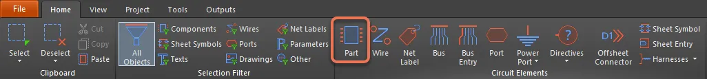
- Right-click in the design space then choose Place » Part from the context menu.
Placement from the Libraries Panel
In the schematic editor, the part selection and placement process can be done from the Libraries panel.
- Use the drop-down at the top of the panel to choose the component type or your favorite component list.
- Use the search field below the top drop-down to filter the list and speed the searching process or scroll and select the required part.
- Click Place, double-click, or click and drag to place the selected component onto the active schematic sheet. While the part is floating on the cursor, it can be rotated (press Spacebar), mirrored along an axis (press X or Y), or edited (press Tab) before placement.
- The columns shown in the list of components in the currently selected library can be reorganized (click and drag).
Graphical Editing
Graphical editing for a part is limited to moving, rotating, and mirroring. When a part is selected in the design space, a dashed selection box will appear around it. To graphically manipulate a selected component:
- Press Delete to remove the selected part.
- Click and hold to move the selected part. The cursor will jump to the nearest electrical hotspot (the wiring end of the nearest pin).
- Press the Spacebar to rotate the part counterclockwise or Shift+Spacebar for clockwise rotation. The action can also be performed while dragging the object. Rotation is in increments of 90°.
- While a part is moving on the cursor, press the X or Y key to mirror it along that axis.
Working Between the Schematic Component and the PCB Component
The software includes tools to help work between the component on the schematic and that same component on the PCB. These tools include cross probing and cross selection.
Cross Probing
As the name implies, Cross Probe allows you to click on a component in one editor and jump to that component in the other editor. To cross probe:
- Click Cross Probe located on the schematic or PCB editor menu on the Tools tab.
- When you click the component in the schematic editor, it will be centered and zoomed in the PCB editor and vice versa.
- The default behavior is to remain in the same editor, ready to cross probe another component. To switch to the other editor as you cross probe, hold the Ctrl key.
Cross Select Mode
Cross Select Mode selects the same component in the other editor. Note that it does not zoom and center. Cross Select Mode is either on or off. Choose Home | Clipboard | Select » Cross Select Mode to toggle the mode on/off. Select multiple components by holding the Shift key as you click to select.
Non-Graphical Editing
This method of editing uses the associated Inspector panel mode to modify the properties of a part object.
During placement, the Component mode of the Inspector panel can be accessed by pressing the Tab key. Once the component is placed, all options appear.
After placement, the Component mode of the Inspector panel can be accessed in one of the following ways:
- If the Inspector panel is already open, select the object, right-click then choose Properties from the context menu.
- With the object selected, choose View | Schematic | Inspector from the main ribbons.
Editing Multiple Objects
The Inspector panel supports multiple object editing, where the property settings that are identical in all currently selected objects may be modified. When multiples of the same object type are selected manually, an Inspector panel field entry that is not shown as an asterisk (*) may be edited for all selected objects.
Part Properties
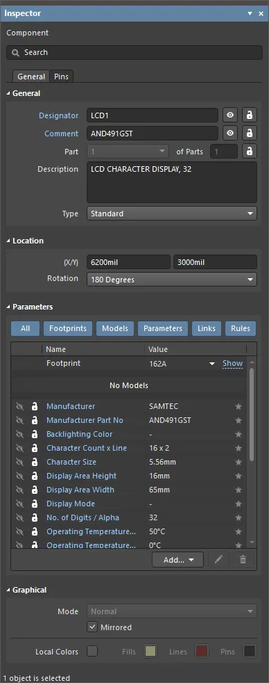
All part object properties are available for editing in the Inspector panel when a placed Part is selected in the design space.
General Tab
Properties
- Designator - toggle the eye icon to show/hide the designator and use the lock icon to lock/unlock the designator. Click the Designator link to open the Designator mode of the Inspector panel and configure as required.

- Comment - toggle the eye icon to show/hide the comment and use the lock icon to lock/unlock the comment. Click the Comment link to open the Parameter mode of the Inspector panel and configure as required.

- Part <x> of Parts - displays the number of the selected part and the total number of parts. Use the drop-down to select the number of the associated part then enter the total number of parts. Click the lock icon to lock/unlock the fields. This field is available only for a multi-part component.
- Description - the part description.
- Type - select one of the following component types for the component footprint here. The available types are:
- Standard - components that possess standard electrical properties and are always synchronized between the schematic and PCB (the footprint, pins/pads and net assignments must all match). An example is a standard electrical component, such as a resistor.
- Mechanical - components that do not have electrical properties and are not synchronized (you must manually place them in both editors). An example is a heatsink.
- Graphical - components that do not have electrical properties and are not synchronized (you must manually place them in both editors). An example is a company logo.
- Net Tie (In BOM) - components that are used to short two or more different nets together and are always synchronized between the schematic and PCB (the footprint, pins/pads and net assignments must all match). They differ from a Standard component in that connectivity created by copper within the footprint is not checked; it is this copper that allows the nets to be shorted. Enable the Verify Shorting Copper option in the Design Rule Checker dialog to verify that there is no unconnected copper within the component.
- Net Tie (No BOM) - components that are used to short two or more different nets together, are always synchronized between the schematic and PCB (the footprint, pins/pads and net assignments must all match), and are not included in the BOM. They differ from a Standard component in that connectivity created by copper within the footprint is not checked; it is this copper that allows the nets to be shorted. Note: enable the Verify Shorting Copper option in the Design Rule Checker dialog to verify that there is no unconnected copper in the component.
- Standard (No BOM) - components that possess standard electrical properties, are always synchronized between the schematic and PCB (the footprint, pins/pads and net assignments must all match), and are not included in the BOM. An example is a testpoint component that you want to exclude from the BOM.
- Jumper - components that are used to include wire links in a PCB design, for example, on a single-sided PCB that cannot be fully routed on one layer. For this component type, the component footprint and pins are synchronized between the schematic and PCB but the net assignments are not, and the component is included in the BOM. As well as selecting this option at the component level, both of the pads in the component must have their JumperID set to the same non-zero value. Jumper type components do not need to be wired on the schematic; they only need to be included on the schematic if they are required in the BOM. If they are not required in the BOM, they can be placed directly in the PCB where the Component Type is set, the JumperIDs are set, and the Nets manually assigned for the pads.
Location
- (X/Y)
- X (first field) - the current X (horizontal) coordinate of the reference point of the object, relative to the current design space origin. Edit to change the X position of the object. The value can be entered in either metric or imperial; include the units when entering a value whose units are not the current default.
- Y (second field) - The current Y (vertical) coordinate of the reference point of the object, relative to the current origin. Edit to change the Y position of the object. The value can be entered in either metric or imperial; include the units when entering a value whose units are not the current default.
- Rotation - use the drop-down to select the rotation.
Parameters
- Parameter selection buttons - click to select the desired parameter. Select All to display all in the grid.
- Grid - lists the Name and Value of the parameters associated with the currently selected component. Use the eye icon to display the parameter and the lock icon to lock/unlock a listed parameter.
- Font - this is available when a parameter is selected in the grid. Click on the displayed font to change the font style.
- Other - this is available when a parameter is selected in the grid. Click to open a drop-down to change additional options:
- Show Parameter Name - enable to show the parameter name.
- Allow Synchronization with Database - enable to synchronize with the database. This option is used to control if the comment can be updated. By default, these options are enabled to always allow synchronization with the source library/database. You may disable this option to prevent that comment from being included in an update process.
- (X/Y) - enter the X and Y coordinates. Choices are: 0°, 90°, 180°, and 270°.
- Autoposition - check to enable auto-positioning, meaning that the text will remain in the chosen position as the component is moved and rotated.
- Add - use the drop-down to select the type of parameter you want to add then configure the Name and Value as needed. Use the pencil icon to edit the selected rule.
Graphical

- Mode - use the drop-down to select the desired mode. If no modes other than Normal are available, this drop-down will be grayed-out.
- Mirrored - enable to mirror the part.
- Local Colors - enable to change the default colors of the desired objects.

This tab lists the Pins and Name for all the pins of the selected component. Use the eye icon to show/hide the pin and the lock icon to lock/unlock the pins. Use ![]() to open the Component Pin Editor dialog.
to open the Component Pin Editor dialog.
Component Pin Editor Dialog

The Component Pin Editor dialog displays all pins for either the component in the active schematic library document or a placed component (or part thereof) in the schematic editor. It provides a single, convenient location for you to modify certain properties of any pin associated to that component. In addition to providing a means of editing pin properties, the dialog also allows you to add new pins or delete existing ones.
Pin Grid
This area presents all pins for the component and descriptive information. The following describes the key fields.
- Footprint Model Mapping - the title of this column is the pad of the indicated linked footprint model to which this pin of the schematic component is mapped. A separate field is presented for each linked footprint model.
- Type - the electrical type of the pin. This type is used when compiling a project or analyzing a schematic document to detect electrical connection errors (using the Electrical Rules Check feature).
-
Owner - the parent part to which the pin is associated. For a single-part component, this entry will always be 1; it is only meaningful for a multi-part component. A multi-part component also includes a non-graphical part, Part Zero. Part Zero is used for pins that are to be included in all parts of the multi-part component, for example, power pins.
- Show - the power pins of multi-part components are typically hidden when their display would otherwise cause unnecessary clutter on the schematic sheet.
- Number - used to determine whether the designator for the pin is displayed (enabled) or hidden (disabled) when the parent part is placed on a schematic sheet.
-
Name - used to determine whether the display name for the pin is displayed (enabled) or hidden (disabled) when the parent part is placed on a schematic sheet.
- Add - click this button to add a new pin to the component. The new pin will be assigned the next available designator (which can be pin 0), and will have the default properties that can be edited.
Right-Click Menu
The key command in the right-click menu is Report, which opens the Report Preview dialog.
Properties Region
This region of the dialog includes the same options and controls as the Pin mode of the Inspector panel.