個別出力および Output Job ファイルによる出力の両方に対応した、幅広い PCB 設計製造用ファイル形式が用意されています。主な形式は次のとおりです。
-
Gerber RS-274X および Gerber X2
-
ODB++
-
IPC-2581
-
NC Drill
-
Board Stack Report
-
プリント系出力:Composite Drill Drawings、Drill Drawing/Guides、Final Artwork Prints、Power-Plane Prints、Solder/Paste Mask Prints
-
Fabrication Testpoint Report
設計の製造に必要な出力ファイルを提供する前に、ボード製造業者に相談して、要求仕様を確認しておくことをお勧めします。
Fabrication 出力は、ファイルの [Add New Fabrication Output] コントロールのメニュー、またはメインメニューの Fabrication Outputs 領域にある Edit » Add Fabrication Outputs サブメニューから、アクティブな Output Job ファイルに追加できます。

OutputJob ファイルを使用すると、設計の出力準備と、その後の高信頼なプロジェクトリリースプロセスによる生成を効率化できますが、アクティブな PCB 設計に対する Fabrication 出力は、PCB エディタの File » Fabrication Outputs サブメニューのコマンドから直接生成することもできます。
NC Drill、Gerber、Gerber X2、ODB++ 出力では、カウンターホールの種類ごとに個別ファイルを生成するのではなく、トップ側すべてとボトム側すべてのカウンターホール用ファイルが生成されます。
Gerber 製造データの生成
Gerber RS274X 形式(Extended Gerber または GerberX とも呼ばれる)の各ファイルは、物理ボード上の 1 つのレイヤー(部品シルク、トップ信号層、ボトム信号層、ソルダーマスク層など)に対応します。このファイル形式には、アパーチャ定義、描画およびフラッシュコマンドの XY 座標位置、その他 PCB 製造に必要な情報が含まれます。
Gerber X2 は、Gerber RS-274X 標準を直接かつ大幅に拡張した進化版であり、PCB 製造および実装のための多くの追加データを提供します。RS-274X 標準と比較して、Gerber X2 形式には、レイヤースタック定義やパッド/ビア属性などの重要な情報が含まれます。Gerber X2 形式の大きな利点は、旧 Gerber RS-274X 標準との後方互換性です。複数ファイルの標準であるため、新標準に移行していない製造/実装業者でも、必要に応じて従来の Gerber ファイル要素を抽出できます。これは、製造ファイル形式の大きな変更に踏み切れない場合や、装置やソフトウェアの柔軟性が低い製造業者にとって大きな利点となり得ます。
ボード設計データを製造・実装業者へ転送する際に Gerber X2 形式を採用する全体的な利点は、ファイルセットに含まれる製造データが非常に豊富であることと、前世代標準との後方互換性により低リスクでアップグレードできることです。CAD-CAM チェーンの両端で完全に実装されていれば、データの誤解釈、ファイルエラー、解釈のばらつきに伴うリスクを大幅に排除できます。要するに、Gerber X2 と IPC-2581 形式は、ボード設計から製造へのデータ転送における新世代のフォーマットです。
プロジェクトの PCB ファイルをアクティブドキュメントにした状態で、メインメニューから File » Fabrication Outputs » Gerber Files または File » Fabrication Outputs » Gerber X2 Files を選択すると、Gerber ファイルセットを生成できます。これにより、エクスポート処理中に適用されるプロットレイヤーおよび一般設定を定義できる適切な Gerber Setup または Gerber X2 Setup ダイアログが開きます。これらのダイアログで提供されるオプションとコントロールの詳細については、以下の折りたたみセクションを参照してください。
このページでは、Gerber Setup および Gerber X2 Setup ダイアログを使用した Gerber ファイル準備について説明します。これらのダイアログは、Advanced Settings ダイアログ で UI.Unification.Gerberダイアログ オプションが有効な場合に使用できます。
UI.Unification.Gerberダイアログ オプションが無効な場合、Gerber ファイル生成は、従来の Gerber Setup および Gerber X2 Setup ダイアログを使用して行われます。

Gerber Setupおよび Gerber X2 Setup ダイアログ
出力は、Project Options ダイアログの Options タブ にある Output Path フィールドで定義された場所に生成されます。生成されるファイル名には、PCB ドキュメント名が含まれます。
生成されたファイルはプロジェクトに追加され、
Projects パネル の
Generated\CAMtastic! Documents および
Generated\Text Documents フォルダ内に表示されます。
生成された Gerber 出力は、複合 CAM ドキュメントとしても開かれ、編集したり現在のプロジェクトに保存したりでき、CAMtastic パネルから管理できます。
生成された CAM 出力を Altium Designer で自動的に開くかどうかを指定するには、
Project Options ダイアログ(
Project » Project Options)の
Options タブ にある
Open outputs after compile オプションを有効にします。
Options and Controls of the Gerber Setup ダイアログ

Gerber Setup ダイアログ。画像上にマウスカーソルを置くと、Layers to plot タブと Advanced タブが切り替わります。
Units
この領域では、生成されるファイルで使用する単位を選択します。
-
Inches – インペリアル単位を使用する場合に有効にします。すべての作業は mil 単位(1 mil = 1/1000 インチ)で行われます。
-
Millimeters – メートル単位を使用する場合に有効にします。すべての作業はミリメートル単位で行われます。
Decimal
この領域のドロップダウンを使用して、Gerber ファイル内のプロット座標の数値精度を指定します。
高い解像度を使用する場合は、PCB メーカーがそのフォーマットをサポートしているか確認してください。0.1、0.01、0.001 mil フォーマットは、グリッド上の穴ピッチが 1 mil より細かい場合にのみ選択する必要があります。
Outputs: FileName.Extension
この領域では、生成される Gerber ファイルの命名方法を選択します。
-
*.gbr – すべてのレイヤーを同じ拡張子 (.gbr) で、ファイル名のみをユニークにして生成します。
-
filename.* (gtl, gbl, gto,...) – すべてのレイヤーを同じファイル名で、拡張子のみを変えて生成します(.gtl、.gbl、.gto など)。
Others
-
Include unconnected mid-layer pads – ミッドレイヤー上の未接続パッドを Gerber プロットに含める場合に有効にします。
-
Generate Reports – 次のファイルを生成する場合に有効にします:
.REP、.EXTREP、.apr、および .APR_LIB。
-
Merge regions and pads inside Footprint – Gerber 出力生成時に、フットプリント内のリージョンとパッドをマージする場合に有効にします。
Layers to Plot タブ
このタブでは、現在の PCB ドキュメントに対して Gerber 出力にプロットするレイヤーを設定できます。
-
Layers List – 現在のPCBで、Gerber出力に利用可能なレイヤーの一覧です。レイヤーは種類ごと(Copper Layers、Silkscreen、Solder Mask、Paste Mask、Mechanical Layers など)にグループ化されます。各レイヤーは次の項目で表示されます。
-
File Name – 個々のGerber出力ファイル名です。名前はプロジェクト名、レイヤー、機能に基づいており、説明的な区切りとしてアンダースコア文字が使用されます。必要に応じてレイヤー名をクリックして新しい名前を入力できます。
-
Layer Name – ボードのレイヤースタックで定義されている、その出力ファイルに適用されるレイヤー名です。
-
Plot – 生成される出力に、そのレイヤーまたはレイヤーグループのGerberプロットを含める場合に有効にします。無効にすると、そのレイヤーのプロットは生成されません。
-
Mirror – ミラーされたGerberファイルを作成したいレイヤーまたはレイヤーグループに対して有効にします。
Mirror 列にアクセスするには、Gerber Setup ダイアログ内で、Advanced Settings ダイアログ の UI.Unification.Gerberダイアログ.ShowMirrorColumn オプションを有効にしておく必要があります。Advanced Settings ダイアログには、Preferences ダイアログの System – General page 上の Advanced ボタンをクリックしてアクセスします。Advanced Settings ダイアログで何らかの変更を行った場合、その変更を有効にするにはソフトウェアを再起動する必要があります。
また、少なくとも1つのレイヤーがミラーとして設定されている場合(たとえば、UI.Unification.Gerberdiarog.ShowMirrorColumn オプションが有効になっている別の Altium Designer インスタンスで)、UI.Unification.Gerberdiarog.ShowMirrorColumn オプションの状態に関係なく、Gerber Setup ダイアログに Mirror 列が表示されます。
リストの最初のレイヤーは Board Outline です。これは、銅箔、シルク、メカニカルレイヤーといった標準的な設計レイヤーではありません。このレイヤーを有効にして生成されるファブリケーションファイルには、Board Profile が含まれます。ここでは、ボードの外形(Board Shape)が、定義された Board Shape に基づいて自動生成される、連続した閉じたパスとして表現されます。Profile には、ボード内に存在する各ボードカットアウトを定義する形状(ポリゴン)も含まれます。
Board Profile は、Gerber および Gerber X2 出力の両方に対して Layers to Plot リスト内で利用できます。必要に応じて、このファイル名はリスト内の他のファイルと同様に変更できます。
PCBエディタでは、メカニカルレイヤーに Layer Type として Board Shape を設定することもできます。このメカニカルレイヤーは、Gerber Setup および Gerber X2 Setup ダイアログで利用可能な Board Profile オプションとは独立しています。Board Shape レイヤーを使用する場合、そのレイヤーには、ボード外形を定義するユーザー定義の閉じた境界と、存在するすべてのボードカットアウトが含まれていなければなりません。Board Shape Layer Type について詳しく学んでください。
► Gerber ファイルフォーマットの詳細については、Ucamco website を参照してください。ボードの Profile については、そのページで入手できる Gerber Format Specification のセクション 6.5 を参照してください。
Layer Name 列ヘッダーの一番右にある

ボタンをクリックすると、
Add Mechanical Layers ダイアログにアクセスでき、すべてのプロットレイヤーに追加するメカニカルレイヤーを選択できます。レイヤーグループに関連付けられた
ボタンをクリックすると、
Add Mechanical Layers ダイアログにアクセスし、選択したレイヤーグループ内のすべてのプロットレイヤーに追加するメカニカルレイヤーを選択できます。
PCBパネル(埋め込みボードアレイ)の Gerber 出力を生成する場合、ダイアログにはパネル用の列と、パネルに含まれる各ボードのレイヤー列が含まれます。この新しい列を使用して、各ボードレイヤーが正しいパネルレイヤーにマッピングされているかを素早く確認できます。

パネルを含む PCB ドキュメントに対する Gerber Setup ダイアログの例。
設計に IPC-4761 タイプが割り当てられたビアが含まれている場合、対応するメカニカルレイヤー(Filling、Capping など)が、レイヤーリスト内の IPC-4761 Via Type Features レイヤーグループの下に表示されます。
Layers to plot リストの一番下には、Layer Classes セクションがあります。レイヤークラス用のチェックボックスを使用すると、特定のレイヤークラスに属するすべてのレイヤーのプロットを一括で有効にできます。ここには、デフォルトのレイヤークラス(Component Layers、Signal Layers、Electrical Layers、All Layers)と、Object Class Explorer ダイアログ で定義されたユーザー定義レイヤークラスが一覧表示されます。

Layer Classes リスト
-
Plot Layers – ドロップダウンを使用してメニューにアクセスし、Layers to plot 領域内のすべてのレイヤーに対する Plot フィールドを一括で有効/無効にできます。
-
Select All – Plot 列のすべてのボックスをオンにします(チェックされたすべてのレイヤーに対して Gerber データが作成されます)。
-
Deselect All – Plot 列のすべてのチェックボックスをクリアします(Gerber データは作成されません)。
-
Select Used – 設計で使用されている、一覧内のレイヤーの Plot 列のすべてのボックスをオンにします。
-
Edit Group – クリックすると Add Mechanical Layers ダイアログが開き、選択したレイヤーグループ内のすべてのプロットレイヤーに追加するメカニカルレイヤーを選択できます。レイヤーグループに関連付けられた ボタンをクリックして Add Mechanical Layers ダイアログにアクセスすることもできます。
-
Mirror Layers – ドロップダウンを使用してメニューにアクセスし、Layers to plot 領域内のすべてのレイヤーに対する Mirror フィールドを一括で有効/無効にできます。
-
Select All – Mirror 列のすべてのボックスをオンにします(チェックされたすべてのレイヤーに対して Gerber データが作成されます)。
-
Deselect All – Mirror 列のすべてのチェックボックスをクリアします(Gerber データは作成されません)。
-
Select Used – 設計で使用されている、一覧内のレイヤーの Mirror 列のすべてのボックスをオンにします。
Advanced Tab
Aperture Matching Tolerances
-
Plus – アパーチャマッチングの正の許容値を定義します。
-
Minus – アパーチャマッチングの負の許容値を定義します。
Leading/Trailing Zeroes
-
Keep leading and trailing zeroes – このオプションを有効にすると、生成される Gerber ファイルに先頭および末尾のゼロがすべて出力されます。
-
Suppress leading zeroes – このオプションを有効にすると、生成される Gerber ファイルに先頭のゼロは出力されません。
-
Suppress trailing zeroes – このオプションを有効にすると、生成される Gerber ファイルに末尾のゼロは出力されません。
Plotter Type
-
Unsorted (raster) – ラスターマシンを使用する場合に選択します(デフォルト)。
-
Sorted (vector) – ベクターマシンを使用する場合に選択します。
Others
-
Optimize change location commands – このオプションを有効にすると、前のオブジェクトから変化しない場合、X または Y の位置データは含まれません。
-
G54 on aperture change – このオプションをオンにすると、アパーチャ変更のたびにプロッタのアパーチャホイールを回転させます。
-
Use software arcs – このオプションをオンにすると、ソフトウェアアークを使用します。
-
Use polygons for octagonal pads – このオプションをオンにすると、八角形パッドにポリゴンを使用します。
-
Generate DRC Rules export file (.RUL) – このオプションをオンにすると、DRC Rules Export ファイル(
.RUL)を生成します。このファイルには、Gerber データが生成される元の PCB ドキュメントの設計ルールの詳細がレポートされます。
Legacy Tab

Gerber Setup ダイアログの Legacy タブ
Film Size
-
X(horizontal) – フィルム長を入力します。
-
Y(vertical) – フィルム幅を入力します。
-
Border size – フィルムのボーダーサイズを入力します。
Position on Film
フィルム上での位置を選択するには、次のオプションを使用します。
-
Reference to absolute origin
-
Reference to relative origin
-
Center on film
Batch Mode
-
Separate file per layer – 各レイヤーごとに個別の Gerber ファイルを生成したい場合に選択します。
-
Panelize layers – パネル化形式で、1つの Gerber ファイルのみを生成したい場合に選択します。
Apertures
-
Embedded apertures (RS274X) – このオプションを有効にすると、RS274X 規格に従ってアパーチャが Gerber ファイルに埋め込まれ、各レイヤーの情報が1つのファイルに含まれます。有効にすると、現在のアパーチャリストに必要なすべてのアパーチャが含まれていることが保証されます。このオプションを無効にすると、この領域の追加コントロールが使用可能になります。
-
Maximum aperture size – 設計で使用するアパーチャの最大サイズを入力します。
-
Generate relief shapes – リリーフスタイルのアパーチャを作成する場合にオンにします。
-
Flash pad shapes – パッド形状をフラッシュする場合にオンにします。
-
Flash all fills – すべてのフィルをフラッシュする場合にオンにします。
-
Apertures List – 現在のすべてのアパーチャデータを一覧表示します。
-
New – ドロップダウンを使用して、新しいアパーチャの追加や、アパーチャリストをアパーチャファイルへ保存/アパーチャファイルから読み込みするためのコマンドメニューにアクセスします。
-
Add Aperture – 新しいアパーチャのプロパティを指定できる
![]() Edit Aperture ダイアログ を開くには選択します。
Edit Aperture ダイアログ を開くには選択します。
-
Load – 読み込むアパーチャファイルの場所を選択するダイアログを開くには選択します。
-
Save – 現在のアパーチャリストに含まれるアパーチャを保存するには選択します。
-
Edit – ドロップダウンを使用して、選択したアパーチャまたはアパーチャリストを編集するためのコマンドメニューにアクセスします。
-
Edit Aperture – 選択したアパーチャのプロパティを
![]() Edit Aperture ダイアログ で編集するには選択します。
Edit Aperture ダイアログ で編集するには選択します。
-
Rename Aperture – 選択したアパーチャのプロパティを Edit Aperture ダイアログで編集するには選択します。
-
Clear All – アパーチャリストからすべてのアパーチャをクリアするには選択します。
-
Create List from PCB – 現在の PCB デザインからアパーチャリストを作成するには選択します。
-
 – 選択したアパーチャを削除するには選択します。
Notes about Apertures
PCB メーカーが埋め込みアパーチャをサポートしていない場合を除き、Embedded apertures (RS274X) オプションを使用することを強く推奨します。最新のフォトプロッタのほとんどは任意サイズのアパーチャを受け付けるラスター型プロッタです。一般的に、埋め込みアパーチャを含む Gerber ファイルも受け付けます。
メーカーが埋め込みアパーチャを使用しない場合は、Gerber ファイルと一緒に別個のアパーチャファイル(*.apt)を含める必要があります。生成されたアパーチャファイルではなく既存のアパーチャファイルを使用する場合、PCB エディタは PCB ドキュメント内のプリミティブ(トラック、パッドなど)を走査し、読み込まれた *.apt ファイル内のアパーチャ記述と照合します。プリミティブに対するアパーチャの完全一致がない場合、PCB エディタは自動的に、適切なより小さいアパーチャでそのプリミティブを paint します。ペイントに適したアパーチャが存在しない場合は、不足しているアパーチャを列挙した *.MAT(マッチ)ファイルが生成され、Gerber ファイルの生成は中止されます。
Gerber ファイルは、NC Drill ファイルと同じフォーマット(精度)で作成する必要があります。たとえば、Gerber ファイルが 0.1 mil フォーマットを使用するように設定されている場合、対応する NC Drill ファイルは 2:4 フォーマットを使用する必要があります。Gerber ファイルがフィルム上の座標位置を絶対原点または相対原点のいずれかを使用するように生成されている場合、NC Drill ファイルも同じ原点基準を使用して生成する必要があります。
Options and Controls of the Gerber X2 Setup ダイアログ

Gerber X2 Setup ダイアログ。画像上にマウスカーソルを置くと、Layers to plot タブと Advanced タブが切り替わります。
Units
この領域では、生成されるファイルで使用する単位を選択します。
-
Inches – インペリアル単位を使用するにはこのオプションを有効にします。すべての作業は mil 単位(1 mil = 1/1000 インチ)で行われます。
-
Millimeters – メートル法単位を使用するにはこのオプションを有効にします。すべての作業はミリメートル単位で行われます。
Decimal
この領域のドロップダウンを使用して、Gerber ファイル内のプロット座標の数値精度を指定します。
フォーマットは、PCB デザイン空間内のオブジェクトの配置精度および/またはファブリケータの好みに合わせて選択します(通常は最高解像度の 0.001 mil または 0.00001 mm に設定します)。
Outputs: FileName.Extension
この領域では、生成される Gerber ファイルの命名オプションを選択します。
-
*.gbr – すべてのレイヤーを一意のファイル名かつ同一の単一拡張子(.gbr)で生成するにはこのオプションを有効にします。
-
filename.* (gtl, gbl, gto,...) – すべてのレイヤーを同一ファイル名かつ異なる拡張子(.gtl、.gbl、.gto など)で生成するにはこのオプションを有効にします。
Others
-
Include unconnected mid-layer pads – ミッドレイヤー上の未接続パッドを Gerber プロットに含めるにはこのオプションを有効にします。
-
Generate Reports – 次のファイルを生成するにはこのオプションを有効にします:
.REP、.EXTREP、.apr、および .APR_LIB。
-
Merge regions and pads inside Footprint – Gerber 出力の生成中に、フットプリント内のリージョンとパッドをマージするにはこのオプションを有効にします。
Layers to plot タブ
このタブでは、現在の PCB ドキュメントに対して Gerber X2 出力でプロットするレイヤーを設定できます。
-
Layers List – 現在の PCB で Gerber 出力に利用可能なレイヤーの一覧です。レイヤーはその種類(Board Outline、Copper Layers、Silkscreen、Solder Mask、Paste Mask、Mechanical Layers、Drills など)ごとにグループ化されています。各レイヤーは次の項目で表示されます。
-
File Name – 個々の Gerber 出力ファイル名です。命名はプロジェクト名、レイヤー、機能に基づき、説明的な区切りとしてアンダースコア文字を使用します。必要に応じてレイヤー名をクリックして新しい名前を入力できます。
-
Layer Name – ボードのレイヤースタックで定義されている、出力ファイルに適用されるレイヤー名です。
-
Plot – 生成される出力に、そのレイヤーまたはレイヤーグループの Gerber プロットを含めるにはこのオプションを有効にします。無効にすると、そのレイヤーのプロットは生成されません。
一覧の最初のレイヤーは Board Outline です。これは銅、シルクスクリーン、メカニカルレイヤーといった標準的な設計レイヤーではありません。このレイヤーが有効な場合に生成されるファブリケーションファイルには、Board Profile が含まれます。ここでは、ボードの外形(Board Shape)が、定義された Board Shape に基づいて自動生成される連続した閉じたパスとして表現されます。Profile には、ボード内に存在する各ボードカットアウトを定義するシェイプ(ポリゴン)も含まれます。
Board Profile は、Gerber および Gerber X2 出力の両方において Layers to Plot リストで利用できます。必要に応じて、このファイル名もリスト内の他のファイルと同様に変更できます。
PCB エディタでは、メカニカルレイヤーに Board Shape の Layer Type を設定することもできます。このメカニカルレイヤーは、Gerber Setup および Gerber X2 Setup ダイアログで利用可能な Board Profile オプションとは独立しています。Board Shape レイヤーを使用する場合、そのレイヤーにはボード外形を定義するユーザー定義の閉じた境界と、存在するすべてのボードカットアウトが含まれている必要があります。Board Shape Layer Type について詳しくは、こちらを参照してください。
Gerber ファイルフォーマットの詳細については、Ucamco website を参照してください。同ページで入手できる Gerber Format Specification のセクション 6.5 を参照すると、Board Profile についてさらに学ぶことができます。
ボタンを
Layer Name 列ヘッダーの一番右にあるボタンをクリックして
Add Mechanical Layers ダイアログにアクセスし、すべてのプロットレイヤーに追加するメカニカルレイヤーを選択します。レイヤーグループに関連付けられた
ボタンをクリックして
Add Mechanical Layers ダイアログにアクセスし、選択したレイヤーグループ内のすべてのプロットレイヤーに追加するメカニカルレイヤーを選択します。
PCB パネル(埋め込みボードアレイ)の Gerber X2 出力を生成する場合、ダイアログにはパネル用の列に加え、パネルに含まれる各ボード用のレイヤー列が含まれます。この新しい列を使用して、各ボードレイヤーが正しいパネルレイヤーにマッピングされているかを素早く確認できます。

パネルを含む PCB ドキュメントに対する Gerber X2 Setup ダイアログの一例。
設計に IPC-4761 タイプが割り当てられたビアが含まれている場合、対応するメカニカルレイヤー(Filling、Capping など)がレイヤーリスト内の IPC-4761 Via Type Features レイヤーグループの下に表示されます。
-
Plot Layers – ドロップダウンを使用して、Layers to Plot 領域内のすべてのレイヤーに対する Plot フィールドを一括で有効または無効にするためのコマンドメニューにアクセスします。
-
Select All – Plot 列のすべてのチェックボックスをオンにするには選択します(チェックされたすべてのレイヤーについて Gerber データが作成されます)。
-
Deselect All – Plot 列のすべてのチェックボックスをオフにするには選択します(Gerber データは作成されません)。
-
Select Used – 設計で使用されている一覧レイヤーの Plot 列のすべてのチェックボックスをオンにするには選択します。
-
Edit Group – クリックして Add Mechanical Layers ダイアログを開き、選択したレイヤーグループ内のすべてのプロットレイヤーに追加するメカニカルレイヤーを選択します。また、レイヤーグループに関連付けられた
 ボタンをクリックして Add Mechanical Layers ダイアログにアクセスすることもできます。
Advanced タブ
Aperture Tolerances
この領域のオプションを使用して、各プロット項目のアパーチャマッチングに使用される許容範囲を設定します。
-
Plus – アパーチャマッチングの正の許容値を定義するために使用します。
-
Minus – アパーチャマッチングの負の許容値を定義するために使用します。
現在のアパーチャリストに項目の完全一致が存在しない場合、ソフトウェアはこの許容範囲内でわずかに小さいまたは大きいアパーチャが存在するかを確認し、存在する場合はそれを代わりに使用します。許容範囲内に適切なアパーチャが存在しない場合、ソフトウェアは必要な形状を作成するために、より小さいアパーチャで「ペイント」しようとします。これには、適切なより小さいアパーチャが利用可能であり、そのアパーチャが「ペイント」に使用できることが条件となります。
アパーチャマッチの許容値は、通常、固定または供給されたアパーチャファイルを必要とするベクターフォトプロッタをターゲットとする場合にのみ使用されます。アパーチャが PCB から作成されて「フラッシュ」されている場合には必要ありません。マッチング許容値が不要な場合は、デフォルトの 0.005 mil のままにしておきます。
Plotter Type
この領域では、ターゲットとするフォトプロッタのタイプを指定します。
-
Unsorted (raster) – ラスターマシンを使用するには選択します(デフォルト)。
-
Sorted (vector) – ベクターマシンを使用するには選択します。
Gerberファイルは、「フィルム」上の位置でソートされたデータ、またはソートされていないデータとして作成できます。ソートが必要なのはベクターフォトプロッタのみであり、初期画像を内部で生成する最新のラスタ方式プロッタには適用されません。ソートを有効にすると、Gerber生成に時間がかかる場合があります。
Gerber X2 Specific
-
File Subject – このフィールドを使用して、Gerber X2出力に
Part 属性として含められるファイルタイプを選択します。ドロップダウンリストには、次の選択肢があります。
-
None
-
Autodetect – ボードファイルの種類に基づいて、以下のリストから属性を自動的に割り当てます。たとえば、単一ボード設計を含むPCBドキュメントには、Single パーツ属性が割り当てられます。
-
Single – 単一PCB。
-
CustomerPanel – ボードアレイまたは出荷用パネル。
-
ProductionPanel – ワーキングパネルまたは製造用パネル。
-
Coupon – クーポン(メインボード設計に関連付けられた性能試験用ボード)。
-
Other – 上記のいずれにも該当しない場合。ファイル内では、属性に付加される文字列によってパーツが非公式に示されます。
-
File Comment – 生成される出力に属性として含めるコメントを入力します。
Others
-
Optimize change location commands – このオプションを有効にすると、前のオブジェクトから変更がない場合、XまたはY位置データは含められません。
-
Generate DRC Rules export file (.RUL) – このオプションを有効にして、DRC Rules Exportファイルを生成します。レポートには、Gerberデータが生成される元のPCBドキュメントに定義されている設計ルールが詳細に記載されます。
ODB++ 製造データの生成
ODB++は、プリント基板の設計および製造に使用されるCAD-to-CAMデータ交換フォーマットです。このフォーマットはもともとValor Computerized Systems, Ltd.によって、PCB設計ソフトウェアと、PCB製造業者が使用するValor CAD-CAMソフトウェアとの間で、より情報量の多いデータ交換を提供できるオープンデータベースとして開発されました。
ODB++ Setup ダイアログでは、ODB++ファイル出力オプションを完全に設定するためのコントロールを提供します。このダイアログには、次のいずれかの方法でアクセスします。
-
OutputJob Configurationファイル内のODB出力ジェネレータを使用する(
*.OutJob)。設定された出力ジェネレータを実行すると出力が生成されます。
-
アクティブなPCBドキュメントで、File » Fabrication Outputs » ODB++ Files をクリックします。ダイアログ内の OK をクリックすると、すぐに出力が生成されます。
PCBから直接出力を生成する際に ODB++ Setup ダイアログで定義された設定は、OutputJob Configurationファイル内で同じ出力タイプに対して定義された設定とは別個かつ独立しています。前者の場合、設定はプロジェクトファイルに保存され、後者の場合はOutputJob Configurationファイルに保存されます。
このページでは、ODB++ Setup ダイアログを使用したODB++出力準備について説明します。このダイアログはODB++バージョン8.1およびレガシーバージョン7.0をサポートします。このダイアログは、ODB.Improvement オプションが Advanced Settings ダイアログ で有効になっている場合に使用できます。
ODB.Improvement オプションが Advanced Settings ダイアログで無効になっている場合、ODB++出力の準備は、ODB++バージョン8.0をサポートする以前のバージョンの ODB++ Setup ダイアログを使用して行われます。
Options and Controls of the ODB++ Setup ダイアログ (Previous Iteration)

Layers to Plot
生成される出力の一部としてプロットしたい各レイヤーの横にあるチェックボックスをオンにします。
 ボタンをクリックして Add Mechanical Layers ダイアログを開き、すべてのプロットまたは選択したプロットに追加するメカニカルレイヤーを選択します。

Add Mechanical Layers ダイアログ
設計にIPC-4761タイプが割り当てられたビアが含まれている場合、対応するメカニカルレイヤー(Filling、Cappingなど)がレイヤーリスト内の IPC-4761 Via Type Features レイヤーグループの下に表示されます。
Units
使用する優先単位としてインチまたはミリメートルを選択します。
File Options
出力ファイル生成に使用したいファイルタイプの横にあるチェックボックスをオンにします。オプションには、非圧縮、.zip、および .tar/.tgz ファイルが含まれます。
TGZファイルは、GZIP圧縮されたTARアーカイブファイルです。TARアーカイブはファイルをまとめるために使用され、その後GZIP圧縮によってファイルサイズが縮小されます。TGZファイルは通常のZipファイルよりも小さくなります。Frontline Genesisなど多くのCAMソフトウェアでTGZファイルが好まれているため、TGZファイルを使用することで製造プロセスを容易にすることができます。
Others
-
Include unconnected mid-layer pads – ODB++プロットのミッドレイヤーで未接続パッドを許可する場合にチェックします。
-
Generate DRC Rules export file (.RUL) - ODB++データが生成される元ドキュメントに定義されているすべての設計ルールを含む
.RUL ファイルを生成する場合にチェックします。
-
Export only the objects inside the board outline - ODB++プロファイルレイヤーを作成するために使用するソースを指定する場合にチェックします。プロファイルレイヤーには、ボードの外形境界が含まれます。既定では、このフィールドは Board Outline に設定されています(ボード形状とも呼ばれ、PCBの境界または外形を定義する閉じた多角形形状です)。各新規PCB作成時に生成されるため、プロファイルレイヤー作成のソースとして最適です。設計にボード形状が関連付けられていない場合、ボードの境界を表す閉じたポリゴンを定義するために使用されたソースPCBレイヤー(例:KeepOutレイヤーや特定のMechanicalレイヤー)を選択できます。このオプションは、ソースドキュメントに埋め込みボードアレイオブジェクトが含まれている場合にのみ使用でき、エクスポートされるオブジェクトの範囲を制御します。オブジェクト(例:テキスト)がボード外形の外側にあっても接している場合、このオプションが有効であれば、そのオブジェクトもエクスポートされる点に注意してください。
-
Merge Net-Tie Nets - 有効にすると、設計内にNet-Tieコンポーネントで接続されたネットがある場合、それらのネットはネットリスト内で区別された単一ネットとしてレポートされます。
-
Distinguish different footprints with the same name - 有効にすると、同じ名前のフットプリントのうち1つが変更された場合、出力内で変更されるのはそのフットプリントのみになります。このオプションが無効な場合、同じ名前を持つすべてのフットプリントが出力内で変更されたものとして表示されます。
-
Generate Additional Tools by Drill Symbols - 有効にすると、定義されたDrill Symbolグルーピングに基づいて追加のドリルツールを生成します。Drill Symbolsグルーピングに存在する場合、追加の列データが追加されます。既存のデータ列は、生成されるドリルデータから削除されません。
Plot Layers
Layers to Plot セクションでドロップダウンを使用するか右クリックして、プロットするレイヤーグループを簡単に選択します。
-
All On - Plot 列のすべてのチェックボックスをオンにします(チェックされたすべてのレイヤーに対してODB++データが作成されます)。
-
All Off - Plot 列のすべてのチェックボックスをオフにします(ODB++データは作成されません)。
-
Used On - プロジェクトで使用されているレイヤーの Plot 列のすべてのチェックボックスをオンにします。
-
Edit Group - Add Mechanical Layers ダイアログを開き、選択したプロットに追加するメカニカルレイヤーを選択します。レイヤーグループに関連付けられた をクリックするか、レイヤーグループを右クリックして Edit Group を選択し、Add Mechanical Layers ダイアログにアクセスすることもできます。
Additional Options
Custom Layers セクション内で右クリックすると、次が表示されます。
-
Add Layer - レイヤーを追加するにはクリックします。
-
Edit Layer - レイヤーを編集するにはクリックします。
-
Delete Layer - レイヤーを削除するにはクリックします。
Custom Layers セクション内のカスタムレイヤーのレイヤーリストセルをクリックすると、Select Layer ダイアログが開き、選択したカスタムレイヤーに追加するレイヤーを選択できます。
Options and Controls of the ODB++ Setup ダイアログ
ODB++ Version
生成される出力をどのODB++バージョンでフォーマットするかを選択します:v. 8.1 またはレガシー v. 7.0 のいずれか。
ODB++バージョン8.1形式の出力を生成する場合、いくつかの機能がサポートされます。
-
Support for layer subtypes – リジッドフレックス PCB 製造をサポートするため、リジッドおよびフレックス層サブタイプに関する情報が含まれます。サポートされている層サブタイプは次のとおりです。
-
COVERLAY – カバーレイ層のクリアランス。
-
STIFFENER – スティフナ材が PCB 上に配置される形状および位置。
-
BEND_AREA – PCB 使用時に曲げられる PCB 上の領域をラベル付けするため。
-
FLEX_AREA – ボードのフレックス部の形状を格納。
-
RIGID_AREA – ボードのリジッド部の形状を格納。
-
SIGNAL_FLEX – フレックス積層板上の信号(銅)層。リジッドフレックス基板において、リジッド積層板上の信号層と区別するために使用されます。
-
PG_FLEX – フレックス積層板上の電源およびグラウンド(銅)層。リジッドフレックス基板において、リジッド積層板上の電源およびグラウンド層と区別するために使用されます。
-
Support for a zones file – リジッドフレックス基板の出力を生成する際、zones ファイルが生成されます。このファイル(生成された出力の \steps\pcb フォルダ内に配置)は、設計内で定義されたすべてのゾーン(ボード領域)に関する情報を含み、関係する層および各ゾーン外形の座標が含まれます。
-
Support for geometry on the stiffener layer – リジッドフレックス基板の出力を生成する際、スティフナ層の形状情報(外形および厚さ)が生成されます( )。
)。
-
Backdrill generation – バックドリルは、正しく処理するために Layer Stack Manager で定義された層の一つ前の層で停止します。
-
Support for a shortf file – shortf ファイルの生成がサポートされています。このファイル(生成された出力の \steps\pcb\eda フォルダ内に配置)は、意図的にショートを許可するネットおよび銅プリミティブ(「Net-Ties」)の一覧を含みます。これにより、製造業者に送付するドキュメントを二重に用意する必要がなくなります。すなわち、製造用にマージされたネットタイを一覧化した ODB++ パッケージと、インサーキットテスト用(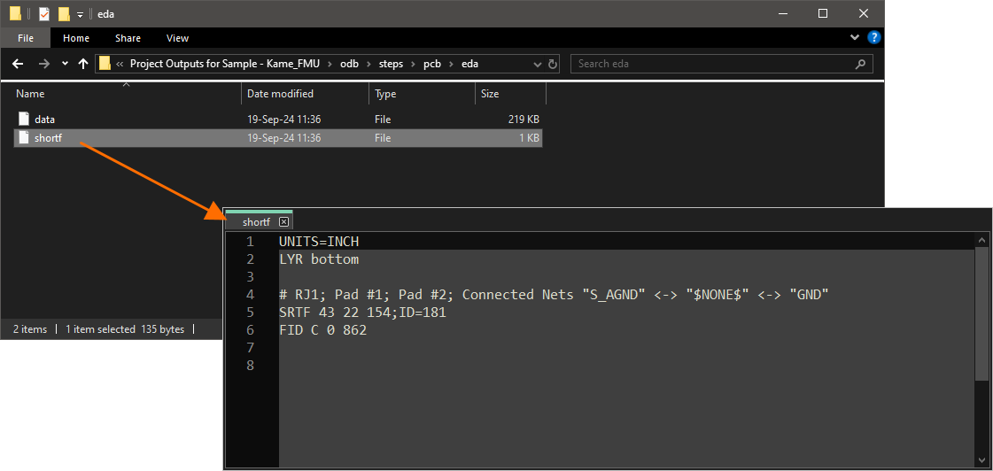 )にマージされていないネットタイを持つ別パッケージを分ける必要がなくなります。
shortf ファイル生成のサポートは、ODB.IntentionalShorts オプションが Advanced Settings ダイアログ で有効化されている場合に利用できます。
-
Support for mid-layer components – ミッドレイヤーに配置されたコンポーネントがエクスポートに含まれます。これは、エクスポートされた ODB++ ファイル内のコンポーネント層データに配置層属性を追加することで提供されます( )。
)。
Units
v. 8.1 オプションが ODB++ Version として選択されている場合、使用する優先単位として Millimeters または Inches のいずれかを選択します。v. 7.0 オプションが ODB++ Version として選択されている場合、Inches がデフォルトで選択され、変更することはできません。
File Options
出力ファイル生成に使用したいファイルタイプの横にあるチェックボックスをオンにします。オプションには、非圧縮、.zip、および .tar/.tgz ファイルが含まれます。
TGZ ファイルは、GZIP で圧縮された TAR アーカイブファイルです。TAR アーカイブはファイルをまとめるために使用され、その後 GZIP 圧縮によってファイルサイズが縮小されます。TGZ ファイルは通常の Zip ファイルよりも小さくなります。Frontline Genesis など多くの CAM ソフトウェアで TGZ ファイルが好まれているため、TGZ ファイルを使用することで製造プロセスを容易に進めることができます。
Others
-
Include unconnected mid-layer pads – ODB++ プロットにおいて、ミッドレイヤー上の未接続パッドを許可する場合にチェックします。
-
Generate DRC Rules export file (.RUL) – ODB++ データが生成される元ドキュメントに対して定義されているすべての設計ルールを含む .RUL ファイルを生成する場合にチェックします。
-
Export only the objects inside the board outline – ODB++ プロファイル層を作成するために使用するソースを指定する場合にチェックします。プロファイル層には、ボードの外形境界が含まれます。デフォルトでは、このフィールドは Board Outline に設定されています(ボード形状とも呼ばれ、PCB の境界または外形を定義する閉じた多角形形状です)。各新規 PCB 作成時に生成されるため、プロファイル層を作成するための最適なソースと言えます。設計に関連付けられたボード形状がない場合、ボードの境界を表す閉じた多角形を定義するために使用されたソース PCB 層(例:KeepOut 層や特定の Mechanical 層)を選択できます。このオプションは、ソースドキュメントに埋め込みボードアレイオブジェクトが含まれている場合にのみ利用可能で、エクスポートされるオブジェクトの範囲を制御します。なお、オブジェクト(例:テキスト)がボード外形の外側にあっても接している場合、このオプションが有効であれば、そのオブジェクトもエクスポートされます。
-
Merge Net-Tie Nets – 有効にすると、Net-Tie コンポーネントで接続されているネットがある設計では、これらのネットはネットリスト内で区別された単一ネットとしてレポートされます。なお、このオプションは Generate shortf: List of Intentional Shorts (Net-Ties) オプションが有効な場合は無効化されます。
-
Generate shortf: List of Intentional Shorts (Net-Ties) – ODB++ バージョン 8.1 形式の出力を生成する場合(v. 8.1 オプションが ODB++ Version として選択されている場合)、意図的にショートを許可するネットおよび銅プリミティブ(「Net-Ties」)の一覧を含む shortf ファイルを生成するには、このオプションを有効にします。生成されたファイルは、ステップ出力の eda サブフォルダ内にあります。なお、このオプションは Merge Net-Tie Nets オプションが有効な場合は無効化されます。
-
Distinguish different footprints with the same name – 有効にすると、同じ名前のフットプリントのうち一つが変更された場合、出力内で変更されるのはそのフットプリントのみになります。このオプションが無効な場合、同じ名前を持つすべてのフットプリントが出力内で変更されたものとして表示されます。
-
Generate Additional Tools by Drill Symbols – 定義された Drill Symbol グループ化に基づいて追加のドリルツールを生成するには有効にします。追加の列データは、Drill Symbols のグループ化内に存在する場合に追加されます。既存のデータ列は、生成されたドリルデータから削除されません。
-
Include Variants Data – ODB++ バージョン 8.1 形式の出力を生成する場合(v. 8.1 オプションが ODB++ Version として選択されている場合)、すべての design variants(
[No Variations] を含む)に関する情報を含めるには、このオプションを有効にします。このオプションが有効な場合、出力には次の情報が含まれます。
-
エクスポートされた任意のバリアント内の各コンポーネントの状態(実装 / 非実装)。
-
エクスポートされた任意のバリアントにおける、コンポーネントレベルでの代替部品に関する情報。
-
バリエーションに応じた各コンポーネントのパラメータ。
-
各バリアント / コンポーネントに適用されたカスタムパラメータ。
このオプションが無効な場合、出力は Outjob ファイルで選択されたバリアント、または PCB エディタから直接出力を生成する場合(File » Fabrication Outputs » ODB++)、Projects パネルで現在アクティブなバリアントに対して生成されます。
-
Outjob ファイルから ODB++ 生成が構成されており、かつ Include Variants Data オプションが有効な場合、Outjob ファイルまたは出力でどのバリアントが選択されているかに関係なく、すべての設計バリアントが ODB++ 出力に含まれます。
-
なお、ペーストマスクのバリエーションは考慮されません。ペーストマスクのバリエーションを含める必要がある場合は、必要なバリアントの設定で Allow Variation for Paste Mask オプションが有効になっていることを確認し、Include Variants Data オプションを ODB++ Setup ダイアログで無効にした状態で、各バリアントごとに個別に出力を生成してください。
プロットするレイヤー
生成される出力の一部としてプロットしたい各レイヤーの横のチェックボックスをオンにします。
ボタンをクリックして Add Mechanical Layers ダイアログを開き、すべてのプロットまたは選択したプロットに追加するメカニカルレイヤーを選択します。
Add Mechanical Layers ダイアログ
設計に IPC-4761 タイプが割り当てられたビアが含まれている場合、対応するメカニカルレイヤー(Filling、Capping など)がレイヤーリスト内の IPC-4761 Via Type Features レイヤーグループの下に表示されます。
プロットレイヤー
ドロップダウンを使用するか、Layers to Plot セクション内で右クリックして、プロットするレイヤーのグループを簡単に選択します。
-
All On - クリックすると、Plot 列のすべてのチェックボックスがオンになり(チェックされたすべてのレイヤーに対して ODB++ データが作成されます)。
-
All Off - クリックすると、Plot 列のすべてのチェックボックスがオフになり(ODB++ データは作成されません)。
-
Used On - クリックすると、プロジェクトで使用されているレイヤーの Plot 列のすべてのチェックボックスがオンになります。
-
Edit Group - クリックすると Add Mechanical Layers ダイアログが開き、選択したプロットに追加するメカニカルレイヤーを選択できます。また、レイヤーグループに関連付けられた をクリックするか、レイヤーグループを右クリックして Edit Group を選択することでも、Add Mechanical Layers ダイアログにアクセスできます。
追加オプション
Custom Layers セクション内で右クリックすると、次が表示されます。
-
Add Layer - クリックしてレイヤーを追加します。
-
Edit Layer - クリックしてレイヤーを編集します。
-
Delete Layer - クリックしてレイヤーを削除します。
Custom Layers セクション内のカスタムレイヤーのレイヤーリストセルをクリックすると Select Layer ダイアログが開き、選択したカスタムレイヤーに追加するレイヤーを選択できます。
埋め込みボードアレイからの生成
埋め込みボードアレイを含む PCB 設計から ODB++ 出力を生成する場合、次の事項が適用されます。
-
設計はレイヤースタック違反について自動的に解析されます。
-
反転された埋め込みボードは、そのレイヤースタックも反転された状態で表示されます。
-
異なるミッドシグナルレイヤーおよび内部プレーンであっても、同じミッドレイヤーパネル上に表示されることがあります。
-
ミッドシグナルレイヤーおよび内部プレーンは互いに反転させることができます。
PCB 設計から ODB++ 出力を生成する際、プロットが有効になっているすべてのレイヤー上のすべてのオブジェクトがエクスポートされます。ボード外形内に存在する設計オブジェクトのみをエクスポートしたい場合は、この境界の外側にオブジェクトを含む追加レイヤーがすべて、プロット無効になっていることを確認してください。
生成された ODB++ ファイルの場所
生成されたファイルの出力パスは、出力の生成方法によって異なります。
-
OutputJobファイルから生成する場合 - 生成されたファイルは、プロジェクトフォルダー内のサブフォルダーに保存されます。名前付けおよびフォルダー構造は、ODB++出力のターゲットとなっているOutput Containerで定義されます。
-
PCBから直接生成する場合 - 出力パスはProject Options - Options ダイアログで指定します。既定では、出力パスはプロジェクトファイルを含むフォルダーのサブフォルダーに設定され、その名前は
Project Outputs for <ProjectName>です。必要に応じて出力パスは変更できます。Optionsタブで各出力タイプごとに個別のフォルダーを使用するオプションが有効になっている場合、ODB++ファイルはさらにその下の ODB++ Outputという名前のサブフォルダーに書き出されます。
生成されたODB++出力を自動的に開く
ODB++出力を生成する際、生成後に新しいCAMドキュメントで自動的に開くよう指定できます。その方法は、出力の生成方法によって異なります。
-
OutputJobファイルから生成する場合 - Output Job Optionsダイアログ内のODB++ Output自動ロードオプションを有効にします(OutputJob Editor からTools » Output Job Options)。
-
PCBから直接生成する場合 - Project OptionsダイアログのOptionsタブでOpen outputs after compileオプションが有効になっていることを確認します(Project » Project Options)。
IPC-2581 製造データの生成
既存のODB++フォーマットに関連するIPC-2581は、Institute for Printed Circuits IPC-2581 Consortium によって2004年に開発されたオープンソース標準であり、その後改訂され、現在のRevision AおよびBリリース(IPC-2581A/B)に至っています。
この標準は、従来のGerber、ドリル、BOM、テキストファイルなどの集合で構成される典型的な製造出力データに代わるものとして、徐々に広く受け入れられてきました。従来の RS-274x Gerberフォーマットには、レイヤースタック、ドリル情報、ネットリストデータ(電気的接続)、BOM情報の定義が欠けているという本質的な制限があるため、複雑な製造ファイルの組み合わせが必要でした。
IPC-2581標準の正式名称は「Generic Requirements for Printed Board Assembly Products Manufacturing Description Data and Transfer Methodology」であり、XMLベースの単一ファイルフォーマットを提供します。このフォーマットには、レイヤースタックアップの詳細から、パッド/配線/コンポーネント情報、部品表(BOM)に至るまで、豊富な基板製造データが含まれます。
単一のIPC-2581 XMLファイルには、次の情報を含めることができます。
-
PCBレイヤーをエッチングするための銅パターン情報
-
基板レイヤースタック情報(リジッドおよびフレキシブル部を含む)
-
ベアボードおよびインサーキットテスト用のネットリスト
-
購買および実装(ピック&プレース)用のコンポーネントBOM
-
製造および実装に関する注記とパラメータ
基板設計データを製造・実装業者へ転送する際にIPC-2581フォーマットを採用することの潜在的な利点は、チェーンの両端で完全に理解される、高度に定義された詳細な単一ファイルフォーマットにあります。CAD-CAMデータ交換の運用システムが確立されれば、データの誤解釈、ファイルエラー、Gerber解釈のばらつきに伴うリスクは大幅に排除されます。要するに、IPC-2581およびGerber X2フォーマットは、基板設計から製造へのデータ転送における新世代のフォーマットと言えます。
プロジェクトのPCBファイルをアクティブドキュメントとして読み込んだ状態で、メインメニューからFile » Fabrication Outputs » IPC-2581を選択すると、IPC-2581ファイルを生成できます。これにより最初にIPC-2581 Configurationダイアログが開き、使用するIPC-2581標準のリビジョン(AまたはB)、およびエクスポート処理で適用される計測単位と浮動小数点数の精度を指定できます。

IPC-2581 Configurationダイアログでエクスポート設定を定義します。
Options and Controls of the IPC-2581 Configuration ダイアログ
-
IPC2581 version - ドロップダウンを使用して正しいIPC-2581バージョンを選択します。
-
Measurement System - ドロップダウンを使用してMetric またはImperial 単位を選択します。
-
Floating Point Precision - 希望する数値を入力するか、矢印キーを使用して希望する浮動小数点精度を選択します。
-
OEMDesignNumberRef - ドロップダウンを使用して使用するコンポーネントパラメータを選択します。DesignItemIDが既定です。
-
Merge Net-Tie Nets - 有効にすると、設計内にNet-Tieコンポーネントで接続されたネットがある場合、それらのネットはネットリスト内で区別された単一ネットとしてレポートされます。
-
Distinguish different footprints with the same name - 有効にすると、同じ名前のフットプリントのうち1つが変更された場合、出力では変更されたフットプリントのみが変更として扱われます。このオプションが無効な場合、同じ名前を持つすべてのフットプリントが出力内で変更されたものとして表示されます。
精度設定は、生成されるIPC-2581準拠ファイル内の位置およびサイズの精度を決定します。以下の画像に例を示します。
と6(右)に設定したIPC-2581ファイルの同一セクション。")
精度を2(左)と6(右)に設定したIPC-2581ファイルの同一セクション。
XMLベースのIPC-2581ファイルは、Project Options ダイアログの Options タブ上のOutput Pathフィールドで定義された場所にエクスポートされます。ファイル名は<PCBDocumentName>.cvgという形式で付けられます。
生成されたファイルはプロジェクトに追加され、
Projects パネルの
Generated\Text Documentsフォルダーの下に表示されます。
NC Drill 製造データの生成
ドリルファイルは、基板製造プロセスにおいてPCBに穴を開けるために使用されます。NC Drillファイルの出力オプションは、NC Drill Setupダイアログを使用して設定します。

NC Drill Setup ダイアログ
NC Drill Setupダイアログには、次のいずれかの方法でアクセスします。
-
OutputJob Configurationファイル内のNC Drill出力ジェネレータを使用する場合(*.OutJob)。設定された出力ジェネレータを実行すると出力が生成されます。
-
アクティブなPCBドキュメントでFile » Fabrication Outputs » NC Drill Filesをクリックします。ダイアログでOKをクリックすると、直ちに出力が生成されます。
PCBから直接出力を生成する際にNC Drill Setupダイアログで定義された設定は、OutputJob Configurationファイル内で同じ出力タイプに対して定義された設定とは別個かつ独立しています。前者の場合、設定はプロジェクトファイルに保存され、後者の場合はOutputJob Configurationファイルに保存されます。
Options and Controls of the NC Drill Setup ダイアログ
-
NC Drill Format – この領域を使用して、NC Drill出力ファイルで使用する単位とフォーマットを指定します。
-
Leading/Trailing Zeroes – ゼロサプレッションは、数値の先頭(リーディング)または末尾(トレーリング)のゼロをすべて削除することで、生成されるデータファイルのサイズを削減する手法です。
-
Keep leading and trailing zeroes – このオプションを有効にすると、生成される NC Drill ファイルに先頭および末尾のゼロがすべて含まれます。
-
Suppress leading zeroes – このオプションを有効にすると、生成される NC Drill ファイルには先頭のゼロが含まれません。
-
Suppress trailing zeroes – このオプションを有効にすると、生成される NC Drill ファイルには末尾のゼロが含まれません。
-
Coordinate Positions
-
Reference to absolute origin – 絶対原点を基準点として使用します。
-
Reference to relative origin – 相対原点を基準点として使用します。
-
Other
-
Optimize change location commands – このオプションをオンにして、位置変更コマンドを最適化します。
-
Generate separate NC Drill files for plated & non-plated holes – このオプションをオンにして、めっき穴と非めっき穴用に個別のドリルファイルを作成します。
-
Generate separate NC Drill files for VIA features – このオプションをオンにして、各 IPC 4761 ビアタイプごとに個別のドリルファイルを作成します。
-
Use drilled slot command (G85) – このオプションをオンにして、複数のドリル穴を使用してスロットを作成します。
-
Generate Board Edge Rout Paths – このオプションをオンにして、ボードカットアウトを含むボード形状を定義するための個別の NC Rout ファイルを作成します。
-
Generate EIA Binary Drill File (.DRL) – このオプションを使用して .DRL ファイルを生成します。DRL はバイナリ形式のドリルファイルです。ブラインドビアおよび/またはベリードビアを含む多層 PCB の場合、各レイヤーペアごとに個別のドリルファイルが作成され、固有のファイル拡張子が付けられます。
NC Drill ファイルは Gerber ファイルと同じフォーマットで作成する必要があります。そうしないと、ドリル位置がパッド/ビア位置と一致しない可能性があります。たとえば、Gerber ファイルが 4:3 フォーマットを使用するように設定されている場合、対応する NC Drill ファイルも同じフォーマットを使用する必要があります。Gerber ファイルが、フィルム上の座標位置を絶対原点または相対原点のいずれかを使用するように設定して生成されている場合、NC Drill ファイルも理想的には同じ原点基準を使用して生成する必要があります。
生成される NC Drill ファイル
| Filename |
Description |
| FileName.DRL |
バイナリ形式のドリルファイル。ブラインドビアおよび/またはベリードビアを含む多層 PCB の場合、各レイヤーペアごとに個別のドリルファイルが作成され、固有のファイル拡張子が付けられます。 |
| FileName.DRR |
ドリルレポート – ツール割り当て、穴サイズ、穴数、ツール移動量の詳細を示します。 |
| FileName.TXT |
ASCII 形式のドリルファイル。ブラインドビアおよび/またはベリードビアを含む多層 PCB の場合、各レイヤーペアごとに個別のドリルファイルが作成され、固有のファイル拡張子が付けられます。 |
| FileName-Plated.TXT |
ASCII 形式のドリルファイル。特に PCB 設計内のめっき穴用です。スロット、角穴、丸穴など、穴タイプごとに個別のファイルが作成されます。 |
| FileName-NonPlated.TXT |
ASCII 形式のドリルファイル。特に PCB 設計内の非めっき穴用です。スロット、角穴、丸穴など、穴タイプごとに個別のファイルが作成されます。 |
| FileName-BoardEdgeRout.TXT |
ASCII 形式のルートファイル。ボードカットアウトを含むボード外形専用です。 |
| FileName.LDP |
ASCII 形式のドリルペアレポート。CAM Editor によるブラインドビアおよびベリードビアの検出に使用されます。 |
生成後、出力はプロジェクトに追加され、Projects パネルの Generated フォルダ配下の、適切に名前が付けられたサブフォルダ内に表示されます。出力タイプごとに個別のフォルダを使用している場合、対応する(個別の)Generated フォルダが Projects パネルに追加されます(例:Generated (NC Drill Output))。
生成された NC Drill ファイルの保存場所
生成ファイルの出力パスは、出力の生成方法によって異なります:
-
OutputJob ファイルから – 生成ファイルはプロジェクトフォルダ内のフォルダに保存されます。名前付けおよびフォルダ構造は、NC Drill File 出力のターゲットとなっている Output Container で定義されます。
-
PCB から直接 – 出力パスは Project Options – Options ダイアログ で指定します。既定では、出力パスはプロジェクトファイルを含むフォルダ配下のサブフォルダに設定され、その名前は Project Outputs for <ProjectName> です。出力パスは必要に応じて変更できます。Options タブで出力タイプごとに個別のフォルダを使用するオプションを有効にしている場合、NC Drill ファイルはさらにその配下の NC Drill Output という名前のサブフォルダに書き込まれます。
生成された NC Drill 出力を自動的に開く
NC Drill 出力を生成する際、出力を新しい CAM ドキュメントで自動的に開くよう指定できます。これを行う方法は、出力の生成方法によって異なります:
-
OutputJob ファイルから – Output Job Options ダイアログ内で NC Drill Output 自動ロードオプションを有効にします(OutputJob Editor から Tools » Output Job Options)。
-
PCB から直接 – Project Options ダイアログの Options タブで Open outputs after compile オプションが有効になっていることを確認します(Project » Project Options)。
Board Stack Report の生成
Altium Designer では、定義されたレイヤースタックおよびスタックアップで使用されているレイヤー(レイヤー名、材料、厚さ、比誘電率)を要約した Board Stack Report を Excel 形式(<PCBDocumentName>.xls)で作成することができます。各スタックの高さも要約されます。Board Stack Report の出力オプションは Layer Stack Report Setup ダイアログを使用して設定し、レポートで表示する単位系および列を指定できます。

Layer Stack Report Setup ダイアログ
上記の Layer Stack Report Setup ダイアログは、Advanced Settings ダイアログ で PCB.ModernBoardStackGenerator オプションが有効になっている場合に使用できます。このオプションが無効な場合は、レポート内の単位系のみを指定できる Layer Stack Report Setup ダイアログが使用可能です( )。
)。
印刷ベースの製造データの生成
次の出力は、ページおよびその上のレイヤーに対して事前定義された設定を持つ印刷ベースの出力です:
-
Composite Drill Guide - 元の PCB ドキュメント用に、事前定義されたコンポジットドリル図面を生成します。
-
Drill Drawings - 元の PCB ドキュメント用に、事前定義された一連のドリル図面およびガイドを生成します。
-
Final - 元の PCB ドキュメント用に、完全な事前定義済み最終アートワーク印刷セットを生成します。
-
Mask Set - 元の PCB ドキュメント用に、事前定義されたソルダ/ペーストマスク図面を生成します。
-
Power-Plane Set - 元の PCB ドキュメント用に、事前定義されたパワープレーン図面を生成します。
Print ダイアログにアクセスして、出力の設定内容を確認および調整します。
Configuring PCB Printouts ページを参照して、詳細を確認してください。
Fabrication Testpoint Report の生成
Fabrication testpoint report ジェネレータは、製造テストポイントとして使用するよう設定されたすべてのパッドおよびビアのレポートを(txt および/または csv および/または IPC-D-356A 形式で)生成します。
Assigning Testpoints on the Board ページを参照して、PCB 設計におけるテストポイントの割り当てについて詳しく学んでください。
テストポイントレポートは、埋め込みボードアレイをサポートします。複数の埋め込みボードアレイを含む PCB ドキュメントからエクスポートする場合、複数の IPC-D-356A ネットリストファイルが生成されます。
Fabrication Testpoint Report の出力オプションは Fabrication Testpoint Setup ダイアログを使用して設定します。

Fabrication Testpoint Setup ダイアログ
Fabrication testpoint report はパッドおよびビアの
Fabrication testpoint 設定のみを使用し、
assembly testpoint report は
Assembly testpoint 設定のみを使用します。Assembly Fabrication Report を設定するために使用される
Assembly Testpoint Setup ダイアログには、
Fabrication Report Setup ダイアログと同じオプションセットがあることに注意してください。
Options and Controls of the Testpoint Setup ダイアログ
レポート形式
-
Text - レポートを標準テキスト形式にする場合に有効にします。
-
CSV - 標準のカンマ区切り値形式(CSV)にする場合に有効にします。Excel などのスプレッドシートアプリケーションにインポートして、さらに処理できます。
-
IPC-D-356A - IPC ネットリストファイルにする場合に有効にします。このファイルには、ブラインドビアおよびベリードビア情報が含まれ、スルーホールビアとフリーパッドを区別します。画像およびドリルデータとともに CAM ドキュメントにインポートすると、PCB 設計で使用されていた元のネット名の復元が容易になり、CAM Editor 内で PCB を理解および管理しやすくなります。
テストポイントレイヤー
これらの選択により、レポートの対象範囲を指定できます:
-
Top layer - ボード上面に割り当てられた有効なテストポイントを含める場合にチェックします。
-
Bottom layer - ボード下面に割り当てられた有効なテストポイントを含める場合にチェックします。
単位
-
Imperial- 座標をインチで出力する場合にチェックします。
-
Metric - 座標をミリメートルで出力する場合にチェックします。
座標位置
-
Reference to absolute origin - テストポイント座標の基準点として絶対原点を使用する場合に選択します。
-
Reference to relative origin - テストポイント座標の基準点として相対原点を使用する場合に選択します。
IPC-D-356A オプション
このダイアログ領域は、IPC-D-356A Report Format オプションが有効な場合にのみ使用できます。
-
Adjacency Information - ショートしている可能性のあるネットの一覧を含める場合にチェックし、隣接条件をテキストボックスに入力します。
-
Board Outline - 特定のネットに接続されていない外形やその他のセグメントタイプのデータの記述を許可するには、このチェックボックスをオンにし、ドロップダウンから目的のデータを選択します。
-
Conductor Traces - 詳細については IPC-D-356A 仕様を参照してください。
-
Merge Net-Tie Nets - 有効にすると、設計内に Net-Tie コンポーネントで接続されたネットが含まれている場合、それらのネットはネットリスト内で区別された単一のネットとしてレポートされます。
生成される製造レポートファイル
生成されるすべてのテストポイントファイルは、まずタイプ(Fabrication または Assembly)、次にファイル名の順で命名されます。たとえば、Fabrication Testpoint Report for BoardFileName のようになります。使用されるファイル拡張子は、有効になっている Report Formats に応じて、.txt、.CSV、.IPC(これは ASCII ファイルであることに注意)です。
生成された製造レポートファイルの保存場所
生成ファイルの出力パスは、出力の生成方法によって異なります:
-
OutputJob ファイルから生成した場合 - 生成ファイルはプロジェクトフォルダ内のサブフォルダに保存されます。名前付けとフォルダ構造は、テストポイント出力のターゲットとなる Output Container で定義されます。
-
PCB から直接生成した場合 - 出力パスは Project Options - Options ダイアログ で指定します。既定では、出力パスはプロジェクトファイルを含むフォルダのサブフォルダで、名前は
Project Outputs for ProjectName です。必要に応じて出力パスを変更できます。Options タブで出力タイプごとに個別のフォルダを使用するオプションが有効になっている場合、テストポイントファイルはさらにその下のサブフォルダ Testpoint Output に書き出されます。
生成された製造レポート出力を自動的に開く
テストポイント出力を生成する際、その出力を新しい CAM ドキュメントで自動的に開くよう指定できます。これを行う方法は、出力の生成方法によって異なります:
-
OutputJob ファイルから生成した場合 - Output Job Options ダイアログ内の IPC-D-356A Output 自動ロードオプションを有効にします(OutputJob Editor から Tools » Output Job Options)。
-
PCB から直接生成した場合 - Project Options ダイアログの Options タブで Open outputs after compile オプションが有効になっていることを確認します(Project » Project Options)。
Output Job ファイルを介した製造ファイル出力
プロジェクトの Output Job Configuration ファイル に製造ファイル出力を含めるには、Fabrication Outputs セクションの下で [Add New Fabrication Output] をクリックし、メニューから出力タイプを選択して、関連するサブメニューから目的のデータソースを選択します。
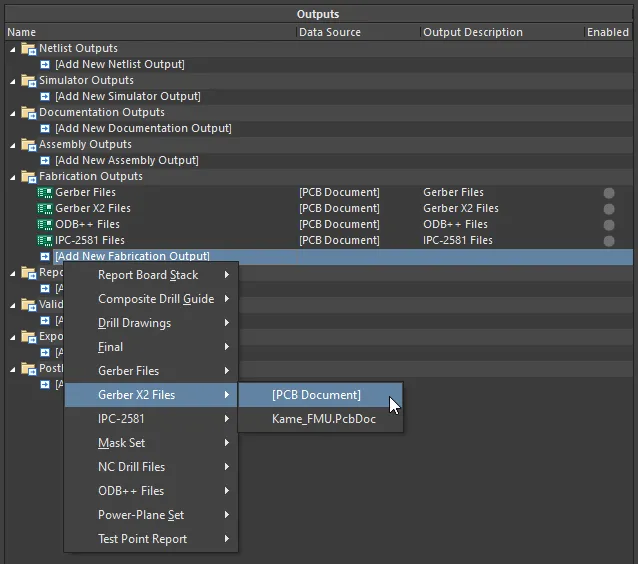
Output Job ファイルの Fabrication Outputs の一部として製造出力を設定します。 ここでは Gerber X2 ファイルの例を示しています。
OutJob を実行すると(手動、または プロジェクトリリースプロセス の一部として)、該当する Output Container に対して定義された設定に従って製造出力が生成されます。

設定済み OutJob の一部として製造出力を準備しているところ。
PCB から直接製造出力を生成する際に関連ダイアログで定義される設定は、同じ出力タイプに対して OutputJob Configuration ファイル内で定義される設定とは別個であり、互いに独立しています。前者の場合、設定はプロジェクトファイルに保存され、後者の場合は OutputJob Configuration ファイルに保存されます。

 AI で翻訳