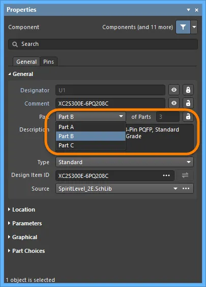
回路図シンボルには通常、コンポーネントの機能を反映できる形状と、1つ以上のピンが含まれます。コンポーネントをどのように表現するか、すなわちシンボルの見た目やコンポーネント・ピンの配置は、設計者に委ねられています。これは、所属組織の要件および採用する設計標準に準拠するように行う必要があります。1つのコンポーネント・シンボルで物理コンポーネント全体を表すこともできますし、コンポーネントを複数のサブパートで定義し、各サブパートが物理コンポーネント内の何らかの論理エンティティを表すようにすることもできます(例:4回路ANDゲート部品における各ANDゲート、またはリレーにおけるコイルと接点セット)。この種のコンポーネントはマルチパート・コンポーネントとも呼ばれます。
新しい回路図シンボルの作成
回路図シンボルは、接続されたWorkspace内で直接作成できます。
-
メインメニューからFile » New » Library を選択し、開いたNew Library ダイアログで、ダイアログのWorkspace 領域からCreate Library Content » Symbol を選択します。

New Library ダイアログを使用して新しいWorkspace Symbolを作成
-
開いたCreate New Item ダイアログで必要な情報を入力し、Open for editing after creation オプションが有効になっていることを確認してOKをクリックします。Workspace Symbolが作成され、一時的な回路図シンボル・エディタが開き、.SchLib ドキュメントがアクティブ・ドキュメントとして表示されます。このドキュメントは、Item-Revisionに従って<Item><Revision>.SchLibの形式で命名されます(例:SYM-001-0001-1.SchLib)。このドキュメントを使用して、以下で説明するようにシンボルを定義します。

Workspace Symbolの初期リビジョンを編集する例 – 一時的な回路図シンボル・エディタは、回路図シンボルを定義するためのドキュメントを提供します。
-
必要に応じてシンボルを定義したら、Projects パネル内のシンボルのエントリ右側にあるSave to Server コントロールを使用してWorkspaceに保存します。Edit Revision ダイアログが表示され、必要に応じてName、Descriptionを変更し、リリースノートを追加できます。保存後、ドキュメントとエディタは閉じられます。
保存したWorkspace Symbolは、Single Component Editing mode またはBatch Component Editing mode のComponent Editorでコンポーネントを定義する際に使用できます。
Workspace SymbolsはComponentsパネルで参照できます。パネル上部の ボタンをクリックしてModelsを選択し、次にSymbols カテゴリを選択して、モデルの表示を有効にします。
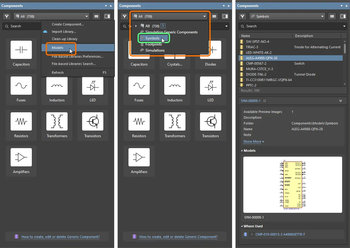
Workspace Symbolを編集するには、Componentsパネルでそのエントリを右クリックし、Editコマンドを選択します。再び一時エディタが開き、シンボルが編集用に開かれます。必要な変更を行い、ドキュメントを保存してWorkspace Symbolの次のリビジョンに反映します。
編集したシンボルをWorkspaceに保存する際、シンボルの現在のライフサイクル状態を保持できます。再保存時( )に表示されるCreate Revisionダイアログで利用できるPreserve lifecycle state (not recommended)オプションにより制御できます。このオプションを有効にすると、新しいシンボル・リビジョンは自動的に前のリビジョンのライフサイクル状態に設定されます。この機能は、Allow to skip lifecycle state change for new revisionsの運用権限が割り当てられているユーザーが利用できます(詳細:Setting Global Operation Permissions for a Workspace)。
Updating Related Component
Workspaceドメイン・モデル(シンボル、フットプリント・モデル、シミュレーション・モデルなど)に変更を加え、その変更をモデルの新しいリビジョンとして保存した瞬間、そのモデルを使用しているWorkspace Componentsは、以前のリビジョンを使い続けるため、実質的に古い状態になります。多くの場合、利用可能な最新リビジョンを使用するように該当モデルへのリンクを更新して、それらのWorkspace Componentsを再保存したいはずです。このプロセスを効率化するため、WorkspaceはAltium Designerと連携し、直接編集機能を通じてモデルに変更を加えた後、Workspaceモデルを再保存する時点で関連コンポーネントを更新できるようにしています。
親コンポーネントに対してこの更新を実行するオプションは、変更したWorkspace Symbolを対象Workspaceへ保存する際に表示されるCreate Revisionダイアログにあります。このオプション(Update items related to <ModelItemRevision>)はデフォルトで有効です。
<ModelItemRevision>Update items related to <ModelItemRevision>はモデルの現在のリビジョン、すなわち関連するWorkspace Componentsが現在使用しているリビジョンです。Workspaceモデル自体を保存すると、これは当然ながら以前(古い)リビジョンとなり、最新ではなくなります。

再保存されるWorkspace Symbolを参照している関連Workspace Componentsを更新するオプションにアクセスしているところ。
関連するすべてのコンポーネントでWorkspace Symbolの現在のリビジョンを使い続けたい場合は、このオプションを無効にします。その場合、Workspaceモデル自体のみが保存されます。
Create RevisionダイアログでOKをクリックすると、変更したシンボルがWorkspaceに保存され、関連する一時エディタは閉じられます。そのWorkspace Symbolを参照しているすべてのWorkspace Componentsは、新しいリビジョンを使用するように自動的に再保存されます(各コンポーネントの次のリビジョンが自動作成され、保存が実行されます)。
-
設計者の観点では、Workspace Componentは、すべての設計ドメインにわたってそのコンポーネントを表現するために必要な情報を、単一のエンティティに集約します。そのため、この意味ではコンテナ、すなわちすべてのドメイン・モデルとパラメトリック情報を格納する「バケット」と捉えることができます。各ドメインでの表現という点では、Workspace ComponentはWorkspaceドメイン・モデルそのものを内包するのではなく、それらのモデルへのリンクを保持します。これらのリンクは、コンポーネント定義時に指定します。
-
回路図シンボルは、既存の旧世代(SchLib、PcbLib、IntLib、DbLib、SVNDbLib)のコンポーネント・ライブラリをインポートする過程で、Workspace内に作成することもできます。このプロセスのインターフェースであるLibrary Importer は、最初に選択したライブラリをWorkspaceへインポートする直感的なフローを提供します。詳細はLibrary Importerを参照してください。
-
新しいWorkspace Symbolは、Component EditorのSingle Component Editing mode でWorkspace Componentを定義する際にも作成できます。
-
シンボルは、file-based schematic symbol library の一部として作成することもできます。
回路図シンボルの定義
回路図シンボルは、コンポーネント本体を表す描画オブジェクトと、実際のコンポーネントの物理ピンを表すピンを配置して作成します。回路図シンボルはAltium Designerの回路図シンボル・エディタで作成します。
シンボル作成に関する注意事項:
-
ライブラリ・エディタに配置したオブジェクトは、配置した順に重なります。ピンがコンポーネント本体の背面に隠れてしまう場合は、Edit » Moveコマンドを使用して表示順序を変更してください。
-
ピンの片側だけが電気的に有効です。この端はホットスポットと呼ばれます。ホットスポット(ピンを持って配置する側の端)がコンポーネント本体から離れるようにしてください。詳細はPin objectを参照してください。
-
回路図ライブラリ・エディタでは、デフォルトのデジグネータや説明など、現在アクティブなシンボルのプロパティは、SymbolモードのPropertiesパネルで編集します。何も選択されていない場合、パネルはこのモードで表示されます。コンポーネント・シンボルの一部として配置したプリミティブをダブルクリックすると、Propertiesパネルには親コンポーネントではなく、そのプリミティブのプロパティが表示されます。
-
シンボル・エディタ・シート(Show Comment/Designator)上でデジグネータとコメントを表示するためのオプションは、PropertiesパネルのLibrary Optionsモードで、現在のライブラリに対して有効/無効を切り替えます。Tools » Document Optionsコマンドを選択して、Propertiesパネルをこのモードで表示します。
-
フォントは、配置時に各オブジェクトごとに個別設定できます。または、PreferencesダイアログのSchematic - Defaults ページ で該当オブジェクトを編集し、新規オブジェクトに使用する好みのフォントを設定できます。
-
Schematic Symbol Generation Toolを使用すると、多ピンのコンポーネントを素早く作成できます。このツールは、右クリックメニューからスプレッドシート経由でピン詳細をインポートすることもサポートします。
-
複数のピンは、SCHLIB Listパネルの右クリックメニューにあるSmart Gridコマンドを使用して、スプレッドシートから現在のシンボルへインポートできます。詳細はこちら。
Workspace Symbolを作成する際は、シンボルのグラフィック(回路図編集ドメインにおける上位レベルのコンポーネント表現)だけを定義すればよい点に注意してください。これは、旧来のファイルベースのコンポーネント管理手法で使用されていた「schematic component」のように、他のモデルやパラメータをその回路図コンポーネントの一部として定義するものではありません。コンポーネントに必要なのは、シンボルのグラフィカルな表現のみです。その他のドメイン・モデルへのリンクやパラメータは、コンポーネント自身の定義の一部として含まれます。
コンポーネントシンボルの作成を始める前に、好みのデフォルト設定を構成しておくための時間を取る価値があります。すべての回路図設計オブジェクト(ライブラリ/シートの両方)のデフォルトは、Preferences ダイアログの Schematic - Defaults ページで設定します。Preferences ダイアログ ページ が開いているときに F1 を押すと、各オプションの詳細情報を確認できます。
設計スペースの準備
コンポーネントシンボルは、常にシート原点(シート中央)付近に描画してください。 必要に応じて、Edit » Jump » Origin(ショートカット J、O)を選択して、シート原点を設計ウィンドウの中央へ移動します。画面左下のステータスバーで、カーソルが原点にあることを確認してください。Altium が提供するコンポーネントは、この点を中心に作成されており、シート中央を通る十字の照準で示されています。コンポーネントは常にこの原点の近くに作成するようにしてください。
回路図上にコンポーネントを配置するとき、コンポーネントはライブラリシンボルのシート原点で「保持」されます。シンボル作成時によく用いられる方法として、コンポーネントのピン1のホットスポットをシート原点に置き、ライブラリから回路図シートへ配置する際にそのピンで保持されるようにします。これは必須ではありません(シンボルのピンやボディのオブジェクトはシート上の任意の場所に配置できます)が、シンボルオブジェクトを原点から離して配置すると、ライブラリから回路図シートへ配置する際に、コンポーネントがカーソルから同じ距離だけ離れた位置に出現することになります。
回路図および回路図ライブラリのグリッドのデフォルト単位はインペリアルです。Altium のコンポーネントはすべてこのインペリアルグリッド上で設計されているため、メトリックのシートグリッドへ切り替える判断が与える影響を理解しておくことが重要です。異なるグリッドで作成されたコンポーネント同士では、正しく配線することが難しくなります。なお、A3 のようなメトリックのシートサイズでもインペリアルグリッドは使用できるため、メトリックサイズのシートで作業するからといってメトリックグリッドへ変更する必要はありません。現在のシートの単位は、Library Options モードの Properties パネル の General region にある General タブで定義します(Properties パネル のこのモードへアクセスするには、メインメニューから Tools » Document Options コマンドを使用します)。

Library Options mode の Properties パネル の General region を使用して、現在のシートの単位を設定します。
必要に応じて、Properties パネル の Show Comment/Designator オプションを有効にし、ライブラリドキュメント内の現在のコンポーネントについて Comment/Designator 文字列を表示します。
オブジェクトは現在のスナップグリッド上に配置されます。現在のグリッドは、設計スペース下部のステータスバー左端に表示されます。
Library Options mode の Properties パネル でも、Snap Grid および Visible Grid を設定できます。 グリッドを変更するたびに Properties パネル を開く代わりに、G を押してスナップグリッドを利用可能な設定間で切り替えることができます。利用可能な設定は、Preferences ダイアログの Schematic – Grids ページで編集できます。
通常、オブジェクトとピンは 100 mil または 50 mil のグリッド上に配置し、10 mil のグリッドが必要になるのは文字列だけです。テキスト文字列の位置合わせを支援するため、文字列を移動中に Ctrl を押すと、グリッドを一時的に最も細かい設定(デフォルトは 10 mil)へ切り替えられます。
Properties パネル
アクティブなドキュメントが Schematic Library ドキュメント(*.SchLib)の場合、メインメニューから Tools » Document Options コマンドを選択します。すると Properties パネル に Library Options が表示されます。以下の折りたたみ可能なセクションには、利用可能なオプションとコントロールに関する情報が含まれています。
Selection Filter
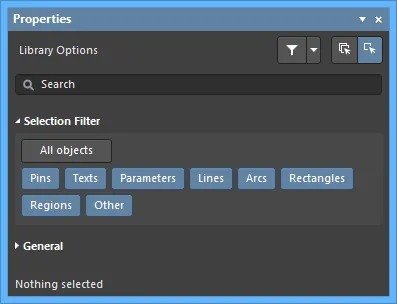
このセクションのオプションは、設計スペースで選択可能な回路図ライブラリオブジェクトを決定します。
-
All Objects button – オブジェクトフィルタリングの解除を選択し、すべての種類のオブジェクトを選択可能にします。
-
Object buttons – 各オブジェクトボタンを切り替えて、そのオブジェクト種別を選択できる/できないを有効化/無効化します。
General
設計オブジェクトを選択すると、パネルにはそのオブジェクト種別に固有のオプションが表示されます。次の表は、ライブラリ設計スペース内に配置可能なオブジェクト種別を示します。リンクをクリックすると、そのオブジェクトのプロパティページにアクセスできます。
回路図シンボルボディの作成
必要に応じて設計スペースのオプションを設定したら、次のステップはコンポーネントのグラフィカル表現、すなわち回路図シート上に配置されたときにそのコンポーネントを表すシンボルグラフィックを作成することです。準拠する回路図シンボルのグラフィック標準を決めておくことが重要です。これにより、シンボルグラフィック設計時の正式なテンプレートが提供され、一貫性のあるレベルが確実に担保されます。Altium の設計手法は標準 IEEE 315 に従っており、最も一般的な回路要素をカバーするだけでなく、半導体要素を組み合わせて多様なシリコンデバイス種別を記号化する方法も明確に定義しています。
シンボルのボディは、Place menu、Utilities bar、または Active Bar を使用して、回路図ライブラリエディタの設計スペースにグラフィカル設計オブジェクトを配置することで作成します。配置した回路図シンボルをダブルクリックして Properties パネル を開き、各形状をさらに定義します。
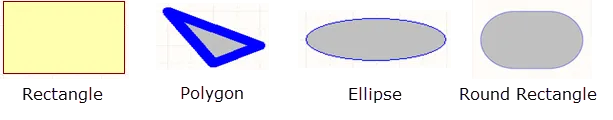
Altium Designer には、以下に示すように、rectangle、polygon、ellipse、round rectangle などのさまざまな閉じたシンボル形状が含まれています。
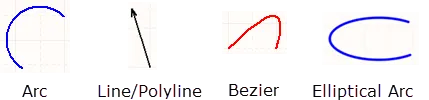
線種の形状には、arc、line/polyline、bezier、elliptical arc があります。line/polyline には矢印のヘッドとテールを含めることができます。ダブルクリックして Properties パネル を開き、ヘッドとテールを定義します。
シンボルへのピン追加
コンポーネントの電気的特性を与え、信号の入出力を行うための接続点を定義するのはコンポーネントのピンです。実際の物理コンポーネント上の各ピンを表すために、ピンを1つずつ配置します。
ピンは、回路図ライブラリドキュメントの設計スペースに現在表示されているコンポーネントに対して、次のいずれかの方法で追加できます。いずれの場合も、ピンは電気端で保持された状態でカーソルに追従して表示されます。必要に応じてピンを回転/反転し、クリックして配置します。
-
Place » Pin コマンド(またはショートカット P, P)を使用します。
-
Active Bar の  ボタンをクリックします。
-
Utilities toolbar の設計オブジェクト・ドロップダウンにある ボタンをクリックします。
-
Component Pin Editor ダイアログ を使用 – 設計スペースでオブジェクトが何も選択されていない場合、Properties パネル を使用してシンボルのプロパティを編集できます。これには、ピンの編集、追加、削除が含まれます。パネルから Component Pin Editor ダイアログ にもアクセスできます。開くには、Properties パネル の Pins タブにある  ボタンをクリックします。 このダイアログは、シンボルに関連付けられた任意のピンの特定プロパティを変更するための、単一で便利な場所を提供します。ピンプロパティの編集手段を提供するだけでなく、新しいピンの追加や既存ピンの削除も行えます。
 作成したシンボルのすべてのピンを管理するための Component Pin Editor ダイアログ にアクセスします。
Options and Controls of the Component Pin Editor ダイアログ
Pin Grid
この領域には、コンポーネントのすべてのピンが表示されます。各ピンについて、次の情報が表示されます。
-
Designator – ピンの数値識別子。パーツの各ピンには一意のデジグネータが必要です。
-
Name – ピンの表示名。名前は任意であり、必要に応じてこのフィールドは空欄のままにできます。あるいは、Name テキストフィールドに文字列を入力し、Name チェックボックスで名前の表示/非表示を切り替えます。
-
Desc – ピンの説明。
-
Footprint Model Mapping – この回路図コンポーネントのピンがマッピングされる、リンクされたフットプリントモデル上のパッド。リンクされた各フットプリントモデルごとに別の列が表示されます。
-
Type – ピンの電気的タイプです。このタイプは、プロジェクトのコンパイル時や回路図ドキュメントの解析時に、電気的接続エラー(Electrical Rules Check 機能)を検出するために使用されます。利用可能なタイプは Input、I/O、Output、Open Collector、Passive、HiZ、Open Emitter、Power です。
-
Owner – ピンが関連付けられている親パートです。単一パートのコンポーネントでは、この項目は常に 1 になります。これはマルチパート・コンポーネントでのみ意味を持ちます。マルチパート・コンポーネントには、非グラフィカルなパート Part Zero も含まれます。Part Zero は、たとえば電源ピンのように、マルチパート・コンポーネントのすべてのパートに含めるピンに使用します。
-
マルチパート・コンポーネントの場合、電源ネットの接続は理想的には Part Zero を使用して割り当てるべきです。ピンを配置した後、Part Number プロパティを
0 に設定すると、そのピンは Part Zero に含まれます。Part Zero に配置されたピンは、すべてのパートに表示されます。
-
必要に応じて、Part Zero に配置したピンを非表示にすることもできます。これは推奨される運用ではありませんが、この方法で電源ネットに接続する必要がある各ピンについて、SCHLIB List パネルまたは SCH List パネルの Hidden Net Name フィールドにネット名を入力し、その後 Component Pin Editor ダイアログ で Show オプションを無効にします(または SCHLIB List パネルもしくは SCH List パネルで Hide オプションを有効にします)。
-
Show – ピンがシート上に表示されている(有効)か、非表示(無効)かを反映します。これは推奨される運用ではありませんが、マルチパート・コンポーネントの電源ピンは、表示すると回路図シートが不必要に煩雑になる場合に非表示にできます。
コンポーネントの非表示ピンは、回路図エディタまたは回路図ライブラリエディタで、Properties パネルの Pins 領域にある Show All Pins オプションを有効にすることでシート上に表示できます。回路図ライブラリエディタでは、Edit メインメニューで Show Hidden Pins オプションも有効にする必要があります。
-
Number – 親パートを回路図シートに配置したときに、ピンのデジグネータを表示(有効)するか非表示(無効)にするかを決定するために使用します。
-
Name – 親パートを回路図シートに配置したときに、ピンの表示名を表示(有効)するか非表示(無効)にするかを決定するために使用します。
ピン名を否定(上にバーを付ける)するには、次のいずれかの方法を使用します。
-
Pin/Pkg Length – ピンのパッケージ長です。
-
Propagation Delay – 伝搬遅延を表示します。これは、信号の先頭が送信側から受信側へ到達するのに要する時間です。
-
Add – このボタンをクリックして、コンポーネントに新しいピンを追加します。新しいピンには次に利用可能なデジグネータ(ピン 0 の場合もあります)が割り当てられ、次のデフォルトプロパティが設定されます。
-
Name –
1
-
Desc – 空白
-
Mapping – すべて
0
-
Type –
Passive
-
Owner – アクティブ/選択中パートの番号。
-
Show/Number/Name – すべて有効。
ダイアログで OK をクリックすると、新しく追加したピンは最初にコンポーネント(またはそのパート)の右下に配置されます。必要に応じて再配置してください。
-
Remove – このボタンをクリックして、現在選択されているピンをコンポーネントから削除します。確認ダイアログが開くので、削除を実行するには Yes をクリックします。回路図上に配置済みのコンポーネント・インスタンスからピンを削除する場合、そのピンに接続されていた既存の配線を引き直す必要があることがあります。
以下は Pin Grid を操作する際のヒントです。
-
親パートにリンクされているモデルのマッピング情報を表示するフィールドを除き、すべてのフィールドは編集可能です。フィールドを 1 回クリックして選択し、値を入力するか必要に応じてオプションを選択します。フィールド外をクリックするか Enter を押して変更を確定します。
-
マルチパート・コンポーネントの場合、アクティブ/選択中パートのピンは通常の白い背景で表示され、他のすべてのパートのピンは灰色の背景で表示されます。
-
ピンは、各列ヘッダーを使用してさまざまなフィールドで並べ替えできます。1 回クリックすると昇順、もう 1 回クリックすると降順に並べ替えます。Shift+Click で追加フィールドによる並べ替えを行います。Ctrl+Click で並べ替えを解除します。
Right-Click Menu
グリッドの右クリックメニューには次のコマンドがあります。
-
Jump – 現在選択されているピンへデザインスペース内でジャンプします(可能な場合、ズームして中央に表示)。
-
Add – コンポーネント(またはそのパート)に新しいピンを追加します。
-
Remove – 現在選択されているピンをコンポーネントから削除します。確認ダイアログが開くので、削除を実行するには Yes をクリックします。
-
Edit – このコマンドは機能しません。
-
Report – Report Preview ダイアログ を開きます。
Properties Region
General Tab
Parameters タブ
-
Parameters – この領域には、現在ピンに定義されているすべてのパラメータが一覧表示されます。
 または
または  アイコンを使用して、設計空間で関連パラメータの値を表示/非表示にします。
 または
または  アイコンを使用して、関連パラメータをロック/ロック解除します。
-
Name – パラメータ名。ルールタイプのパラメータの場合、このエントリは
Rule としてロックされます。
-
Value – パラメータ値。ルールタイプのパラメータの場合、このエントリにはルールタイプと、定義された制約の一覧が反映されます。
-
Font – クリックするとメニューが開き、必要に応じてフォント、フォントサイズ、色、太字、斜体などの属性を選択できます。
-
Other – クリックするとドロップダウンが開き、追加オプションを変更できます:
-
Show Parameter Name – パラメータ名を表示するには有効にします。
-
Allow Synchronization with Database – データベースと同期するには有効にします。
-
X/Y – X および Y 座標を入力します。
-
Rotation – ドロップダウンを使用して回転を選択します。
-
Autoposition – 自動配置を有効にするにはチェックします。
-
Add – クリックしてパラメータを追加します。
 を使用して、現在選択されているパラメータを削除します。
multi-part component の場合、選択したパートに関連するピンが
Component Pin Editor ダイアログ内でハイライト表示されます。他のパートのすべてのピンはグレー表示になります。
Component Pin Editor ダイアログは、配置済みコンポーネント(またはその一部)に対して、Schematic Editor からもアクセスできます。
ピンプロパティの設定
Tab を押して Properties パネルの Component モードを開き、配置前にピンプロパティを編集します。数値は、以降のピン配置で自動的にインクリメントされます。自動インクリメントの動作は、Preferences ダイアログの Schematic – General ページにある Auto-Increment During Placement 設定で構成します。負の値を使用すると自動デクリメントになります。

Preferences ダイアログの Schematic - General ページを使用して、自動インクリメントの動作を定義します。 配置中、またはピンを移動するたびに、ピンは電気端(ピンのホットエンドとも呼ばれます)を持って保持されます。電気端がコンポーネント本体から離れるようにピンを配置する必要があります。移動中にスペースバーを押すとピンを回転できます。
ピンは、電圧レギュレータのタブのような、コンポーネント上の電気機械的ポイントを表すために配置することもできます。
ピンには Name や Designator などの複数のプロパティがあります。PCB フットプリントのパッドにシンボルのピンを対応付けるのに使用されるのは、ピンの Designator です。ピンの端から Designator と Name が表示されるデフォルト距離は、Schematic および Schematic Library エディタ全体に共通のシステム設定です。Preferences ダイアログの Schematic – General ページで Pin Margin を設定します。
Name の個別設定は、Component Pin Editor ダイアログで構成できます。
ピンには、Altium の電気ルールチェックシステムがピン同士の接続が有効かどうかを検証するために使用する Electrical Type があります。このオプションは、Component Pin Editor ダイアログで、そのコンポーネントピンの電気タイプに合わせて設定します。デフォルトの Pin Length は、選択したスナップグリッド(通常 100 mil または 50 mil)に適合するはずです。デフォルト長は 30 で、一般的な長さは 20 または 30 です。
Symbols Component Pin Editor ダイアログでは、ピンからの電気情報を表すために、Pin のさまざまな位置に追加できます。
Pin

回路図の Pin は、回路図設計空間における物理コンポーネントのピンを表します。
概要
ピンは電気設計プリミティブです。ピンはコンポーネント(パート)に電気的特性を与え、入出力信号のための接続点を定義します。
利用可能範囲
ピンは、以下のいずれかの方法で、回路図ライブラリエディタにのみ配置できます:
-
メインメニューから Place » Pin をクリックします。
-
Utilities ツールバー(
 )のドロップダウンで
  をクリックします。
-
右クリックして、コンテキストメニューから Place » Pin を選択します。
配置
コマンドを起動すると、カーソルが十字に変わり、ピン配置モードに入ります。配置は、次の一連の操作で行います:
-
クリックするか Enter を押して、ピンを固定します。フローティング状態のピンは電気的端子側で保持されており、この端子はコンポーネント本体から離れる向きに配置する必要がある点に注意してください。ピンの片側だけが電気的端子であり、常にこの端子側が保持されます。
-
追加のピンを続けて配置するか、右クリックするか Esc を押して配置モードを終了します。
配置中(ピンがカーソルに追従して浮いている状態で、かつピンの電気的端子側を固定する前)に実行できる追加操作は次のとおりです。
-
Tab キーを押して配置を一時停止し、Propertiesパネルの Pin mode にアクセスします。ここでプロパティをその場で変更できます。配置を再開するには、デザインスペースの一時停止ボタンのオーバーレイ(
 )をクリックします。
-
Alt キーを押すと、移動方向を(最初の移動方向に応じて)水平軸または垂直軸に制限します。
-
Spacebar を押すとピンを反時計回りに回転し、Shift+Spacebar で時計回りに回転します。回転は90°刻みです。
-
X または Y キーを押して、ピンをX軸またはY軸に沿ってミラーします。
ライブラリコンポーネントは、Library Editorシートの原点(中心)付近に作成します。原点は濃い十字のガイド線で示されています。通常は、ピンまたはコンポーネント本体の角をシート原点に配置します。
ピン番号(Designator)は、接続性を確立するために使用されるため、必ず定義する必要があります。Electrical Type も重要で、Schematic EditorでElectrical Rules Check(ERC)に使用されます。
ピン番号付けに関する注意
多くのコンポーネントでは、数値の名前と番号を持つピンが連番で存在します。Preferencesダイアログの Schematic – General ページ にある Auto-Increment During Placement 機能を使用すると、これらのピン配置を高速化できます。配置前にピンプロパティを編集すると(ピンがカーソル上でフローティングしている間に Tab を押す)、自動インクリメントが自動的に呼び出されます。この機能は Designator と Name の両方で動作します。ピンの Designator は Primary の自動インクリメントフィールドを使用し、ピンの Name は Secondary の自動インクリメントフィールドを使用します。アルファベットおよび数値の昇順、ならびに数値の降順に対応しています。

Preferencesダイアログの Schematic – General ページで Auto-Increment During Placement 設定を構成します。

アルファベットのピン名が増加し、数値のピン番号が減少している点に注意してください。
グラフィカル編集
ピンを移動するには、クリックして押したままにします。カーソルがピンの電気的ホットスポット端にジャンプするので、新しい位置へ移動し、電気的端子側がコンポーネント本体から離れる向きになるように配置します。
ドラッグ中に、ピンは回転(Spacebar/Shift+Spacebar)またはミラー(X または Y キーでX軸またはY軸に沿ってミラー)できます。
非グラフィカル編集
Pin ダイアログまたはPropertiesパネルによる編集
Properties ページ: Pin Properties
ピンのプロパティは Pin ダイアログおよび Properties パネルで編集できます。これにより、デザインスペースで現在選択されているすべてのアイテムを編集できます。
ピン表示名とデジグネータ – 位置とフォント
ピンの表示名およびピンのデジグネータ(番号)の位置は、Preferencesダイアログの Schematic – General ページ にある Pin Margin 設定によってグローバルに定義されます。これは環境設定であり、設定を定義したPCに適用されます。これらの設定は、ピンの非電気的端子側からテキストが離れる相対距離を定義します。
の距離を設定します。")
Preferencesダイアログでピンテキスト(Pin Margin)の距離を設定します。
回路図ライブラリドキュメントのデフォルトのシステムフォントは Times New Roman, 10pt, Regular です。これは固定で変更できません。ライブラリコンポーネントを回路図シートに配置すると、この同じデフォルトフォントが適用されますが、固定ではなく必要に応じて変更できます。なお、回路図シートで使用されるシステムフォントは、Power Ports、Ports、回路図シート枠内のX/Yリージョンマーカーなど、他のオブジェクトにも適用されます。
ピンについては、これらのシステムレベルの位置およびフォント設定を上書きできます。ピンの Designator および Name の位置とフォントをカスタマイズするためのコントロールは、Propertiesパネルの Pin モードにあります。
および Name のフォントと位置を変更できます。")
必要に応じて、個々のピンの Designator(番号)および Name のフォントと位置を変更できます。
Custom Position オプションを使用して、位置のデフォルト設定を上書きするカスタム位置に変更します。Margin については、関連フィールドに新しい値を直接入力します。Orientation については、ドロップダウンで角度(0° または 90°)と To 参照(Pin または Component)を選択します。
Custom Settings オプションを使用して、デフォルトのシステムフォントの使用から、上書きするカスタムフォントの使用に切り替えます。
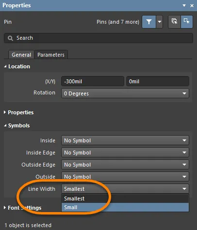
ピンシンボルの線幅
回路図編集ドメインでコンポーネントを表現する際、そのデバイスの回路図シンボルの一部として定義された各ピンには、1つ以上のシンボルを表示できます。これらは、必要に応じて、メインのコンポーネントシンボル外形に対して Inside、Inside Edge、Outside、Outside Edge の位置に表示されるシンボルです。例としては、Inside Edge の Clock シンボルや、Outside Edge の Dot シンボルなどがあります。こうしたシンボルは、特定のピンを通過する信号の目的を視覚的に示すことで、設計の可読性を大幅に向上させます。
Propertiesパネルの Symbols 領域にある Line Width 設定を使用して、これらのシンボルを描画する線の幅を指定します。Small または Smallest から選択します。
古い設計では、適切な電源ネットに接続された非表示の電源ピンを持つコンポーネントが含まれていることがあります。この方法は推奨されませんが、非表示ピンは SCHLIB List または SCH List パネルの Hidden Net Name フィールドにネット名を入力することで接続できます。
Pin Properties
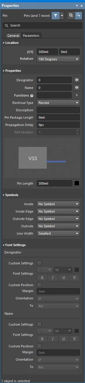
Generalタブ
Location
-
(X/Y)
-
X (第1フィールド)– 現在のデザインスペース原点に対する、オブジェクト参照点の現在のX(水平)座標です。編集してオブジェクトのX位置を変更します。値はメートル法またはヤード・ポンド法のいずれでも入力できます。現在のデフォルトと異なる単位で値を入力する場合は、単位を含めてください。
-
Y (第2フィールド)– 現在の原点に対する、オブジェクト参照点の現在のY(垂直)座標です。編集してオブジェクトのY位置を変更します。値はメートル法またはヤード・ポンド法のいずれでも入力できます。現在のデフォルトと異なる単位で値を入力する場合は、単位を含めてください。
-
Rotation – ドロップダウンを使用して回転を選択します。
Properties
-
Designator – ピンの数値識別子です。パーツ内の各ピンは一意のデジグネータを持つ必要があります。親パーツを回路図シートに配置したときに、ピンの Designator を表示するか非表示にするかを
 または
または  で(それぞれ)指定します。
-
Name – ピンの任意の表示名を指定するために使用します。デフォルトでは、新規に配置したピンはデジグネータ値を使用して命名されます。表示名を指定すると、特にICタイプのコンポーネントで有用で、意味のある名前によりピンの用途を素早く把握できます。親パーツを回路図シートに配置したときに、ピンの Name を表示するか非表示にするかを または で指定します。
ピン名を否定(上にバーを付ける)するには、次のいずれかの方法を使用します。
-
Function – このフィールドを使用して、編集中の多機能ピンに対して複数の名前(機能)を指定します。ピンの代替名を入力し、Enter を押すか、フィールド右側の  ボタンをクリックします。追加された代替名は、フィールド下にラベルとして表示されます。機能のラベル内の「
x」をクリックすると削除できます。
-
このフィールドに制限はなく、数字や特殊文字(&、*、% など)も使用できます。
-
カスタム名に対するすべての Font Settings は、元のピン名と同じです。
-
コンポーネントを回路図シートに配置した後、ピン名として表示する機能は、Component mode の Properties パネル の Pins タブで選択できます。
-
Electrical Type – ドロップダウンを使用してピンの電気的タイプを設定します。これは、プロジェクトのコンパイル時や回路図ドキュメントの解析時に、電気的接続エラーを検出するため(Electrical Rules Check機能を使用)に用いられます。
-
Description– 必要に応じて、ピンの説明を分かりやすく入力します。
-
Pin Package Length – ピン-パッケージ長を入力します。Enter を押すと、単位が自動的に付加されます。
-
Propagation Delay – このフィールドには伝搬遅延が表示されます。これは、信号の先頭が送信側から受信側へ到達するまでに要する時間です。
-
Part Number – ピンをマルチパート部品に追加している場合に使用できます。上下矢印を使って、ピンを関連付けるパートを指定します。マルチパート部品には、非グラフィカルなパート(Part Zero)も含まれます。Part Zero は、電源ピンなど、マルチパート部品のすべてのパートに含めるピンに使用します。
-
Pin Length – 現在定義されている測定単位に従ってピンの長さを指定します。カラーボックスをクリックしてピンの色を編集します。
Symbols
これらのシンボルは純粋にグラフィカルなものです。ピンの真の電気的特性は、ピンの Electrical Type に設定されたエントリによって決まります。
-
Inside – 必要に応じて、部品グラフィックの内側にピン用シンボルを追加します。
-
Inside Edge – 必要に応じて、部品グラフィックの内側エッジにピン用シンボルを追加します。
-
Outside Edge – 必要に応じて、部品グラフィックの外側エッジにピン用シンボルを追加します。
-
Outside – 必要に応じて、部品グラフィックの外側にピン用シンボルを追加します。
-
Line Width – シンボル描画に使用する線の太さを決定します。これは、これらのシンボルの線幅を部品シンボルの描画線幅と同一にすることを規定する GOST 規格への対応を支援します。
Line Width設定は、ピンの定義されたElectrical Typeに関連して使用される自動シンボルにも適用されます。
Font Settings
-
Designator
-
Custom Settings – 有効にすると、下の Font Settings にアクセスしてフォントをカスタマイズできます。
-
Font Settings – コントロールを使用して、フォント、フォントサイズ、色、太字や下線などの特殊設定を構成します。
-
Custom Position – 有効にすると、下のコントロールにアクセスして位置をカスタマイズできます。
-
Margin – 希望するマージンを入力します。
-
Orientation – ドロップダウンから向きを選択します。
-
To – ドロップダウンからデジグネータの対象オブジェクトを選択します。
-
Name
-
Custom Settings – 有効にすると、下の Font Settings にアクセスしてフォントをカスタマイズできます。
-
Font Settings – コントロールを使用して、フォント、フォントサイズ、色、太字や下線などの特殊設定を構成します。
-
Custom Position – 有効にすると、下のコントロールにアクセスして位置をカスタマイズできます。
-
Margin – 希望するマージンを入力します。
-
Orientation – ドロップダウンから向きを選択します。
-
To – ドロップダウンから名前の対象オブジェクトを選択します。
Parameters Tab
Parameters
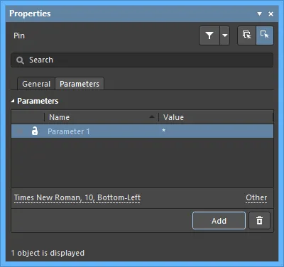
この領域を使用して、現在選択されているピンオブジェクトに付随するパラメータを管理します。
-
Grid – この領域には、現在ピンに定義されているすべてのパラメータが一覧表示されます。 または
 アイコンを使用して、設計スペース内で関連パラメータの値を表示/非表示にします。
 または アイコンを使用して、関連パラメータをロック/ロック解除します。
-
Name – パラメータ名。ルールタイプのパラメータの場合、このエントリは
Rule としてロックされます。
-
Value – パラメータ値。ルールタイプのパラメータの場合、このエントリにはルールタイプと、定義された制約の一覧が反映されます。
-
Font – クリックするとメニューが開き、必要に応じてフォント、フォントサイズ、色、太字、斜体などの属性を選択できます。
-
Other – クリックするとドロップダウンが開き、追加オプションを変更できます:
-
Show Parameter Name – 有効にすると、Schematic Library エディタ内でパラメータ名を表示します。
-
Allow Synchronization with Database – 有効にすると、データベースと同期します。このオプションは、コメントを更新可能かどうかを制御するために使用します。既定では、ソースライブラリ/データベースとの同期を常に許可するため、これらのオプションは有効になっています。このオプションを無効にすると、そのコメントが更新プロセスに含まれないようにできます。
-
X/Y – 希望する X および Y 座標を入力します。
-
Rotation – ドロップダウンから回転を選択します。
-
Autoposition – チェックすると自動配置が有効になります。つまり、部品を移動・回転してもテキストは選択した位置に留まります。
-
Add – クリックしてパラメータを追加します。 を使用して、現在選択されているパラメータを削除します。
古い設計では、適切な電源ネットに接続された非表示の電源ピンを持つ部品が含まれていることがありました。この方法は推奨されませんが、非表示ピンは SCHLIB List または SCH List パネルの Hidden Net Name フィールドにネット名を入力することで接続できます。
Pasting Array
標準の切り取り/コピー/貼り付けコマンド に加えて、部品シンボル作成時にメインメニューの Edit » Paste Array コマンドを使用して、現在のクリップボード内容を現在のドキュメントへ、縦方向または横方向のオブジェクト配列として配置することもできます。これは、作成中の部品シンボルに複数のピンを含める必要がある場合に特に便利です。
コマンドを起動すると、Setup Paste Array ダイアログが表示されます。

Setup Paste Array ダイアログ
Options and Controls of the Setup Paste Array ダイアログ
Placement Variables
-
Item Count - ワークスペースに貼り付ける重複アイテムの総数を指定します。
-
Primary Increment - 増分量を指定します。数値を増分するには、増分ステップを整数値として入力します。アルファベット順に増分するには、スキップしたい文字数を表すアルファベットの文字を入力します。たとえば初期テキストが 1A の場合、1 ずつ増分するにはフィールドを A(アルファベットの最初の文字)に設定します。フィールドを C(アルファベットの 3 番目の文字)に設定すると、テキストは 1A、1D(A の 3 文字後)、1G…となります。貼り付けるオブジェクトがピンの場合、このフィールドは Pin Designator に影響します。
-
Secondary Increment - このフィールドはピンオブジェクトの配列を貼り付ける場合にのみ適用され、Pin Display Name に影響します。Primary Increment フィールドに従って増分量を指定するために使用します。
数値の場合、増分は昇順または降順にできます。Primary Increment および/または Secondary Increment フィールドに、昇順の場合は正の整数、降順の場合は負の整数を入力します。
-
Remove Leading Zeroes - このオプションを有効にすると、貼り付け配列テキストから先頭のゼロを削除します。標準のテキスト文字列では、これは文字列の数値部分の先頭ゼロのみに関係し、英字の前に付くゼロは削除しません。たとえば、テキスト文字列 C000020 は(Primary Increment 1 の場合)C21 として貼り付けられ、テキスト文字列 000C000020 は 000C21 として貼り付けられます。ピンオブジェクトを貼り付ける場合、これは Pin Designator のみに関係し、Pin Display Name には関係しません。
Spacing
-
Horizontal - このフィールドに値を入力して、配列アイテムごとの水平方向の移動量を決定します。正の値はカーソル位置の右側に配列を配置します。負の値は左側に配置します。
-
Vertical - このフィールドに値を入力して、配列アイテムごとの垂直方向の移動量を決定します。正の値はカーソル位置から上方向に配列を配置します。負の値は下方向に配置します。
必要に応じて各種オプションを設定し、OK をクリックします。
間隔(Spacing)には正または負の値を入力し、横方向配置では配列を右側/左側のどちらに貼り付けるか、縦方向配置では上方向/下方向のどちらに貼り付けるかを決定します。
ドキュメント上で配列を挿入する開始位置の選択を求められます。カーソルを目的の位置に合わせてクリックするか、Enter を押します。配列は選択した開始位置に貼り付けられます。
Adding IEEE Symbols
ロジック機能またはデバイスを表現するために、回路図シンボルで IEEE シンボルを使用できます。これらのシンボルにより、ユーザーは内部特性に関する特別な知識がなくても、これらの機能やデバイスのロジック特性を理解できます。
配置可能な IEEE シンボルを以下の画像に示します。
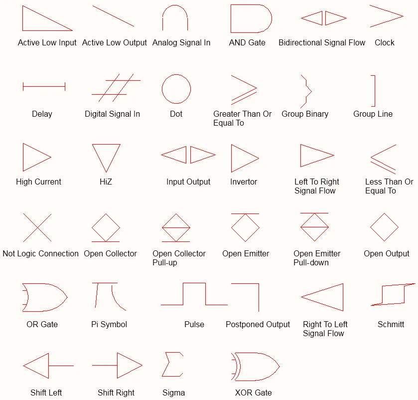
IEEE Symbols
")
配置された IEEE シンボル(Sigma)
概要
IEEE シンボルは非電気的な描画プリミティブです。ロジック機能またはデバイスを表現するために使用されます。これらのシンボルにより、ユーザーは内部特性に関する特別な知識がなくても、これらの機能やデバイスのロジック特性を理解できます。
使い方
IEEE Symbol オブジェクトは、Schematic Library Editor でのみ配置できます。配置可能なシンボルは合計 34 種類で、次の方法で配置できます:
-
メインメニューから Place » IEEE Symbols を選択します。
-
右クリックして、コンテキストメニューから Place » IEEE Symbols を選択します。
-
Utilities ツールバーの
 ボタンをクリックします。
-
Active Bar で Place IEEE Symbol を選択します(
Open Collector シンボルが配置されます)。
配置
コマンドを起動すると、カーソルが十字(クロスヘア)に変わり、IEEEシンボル配置モードに入ります。選択したIEEEシンボルがカーソル上に浮いた状態で表示されます。
-
オブジェクトを所定の位置に合わせてから、クリックするか Enter を押して配置を確定します。
-
続けて別のシンボルを配置するか、右クリックするか Esc を押して配置モードを終了します。
配置中に実行できる追加操作は次のとおりです。
-
Tab キーを押して配置を一時停止し、Properties パネルの IEEE Symbol モードにアクセスします。ここでプロパティをその場で変更できます。配置を再開するには、デザインスペースの一時停止ボタンのオーバーレイ()をクリックします。
-
Spacebar を押すとオブジェクトを反時計回りに回転し、Shift+Spacebar を押すと時計回りに回転します。回転は90°刻みです。
-
X または Y キーを押して、シンボルをX軸またはY軸に沿ってミラー反転します。
-
(テンキーの)+ または - キーを押して、シンボルを拡大または縮小します。
グラフィカル編集
この編集方法では、配置済みのIEEEシンボルオブジェクトをデザインスペース上で直接選択し、位置や向きをグラフィカルに変更できます。IEEEシンボルは形状が固定されており、サイズ変更は該当するキーボードショートカットでのみ可能です。そのため、IEEEシンボルオブジェクトを選択しても編集ハンドルは表示されません。
")
選択されたIEEEシンボル(Sigma)
破線のボックス内を任意の場所でクリックしてドラッグし、必要に応じてシンボルを再配置します。ドラッグ中に、回転(Spacebar/Shift+Spacebar)、ミラー(X または Y キーでX軸/Y軸に沿ってミラー)、サイズ変更(テンキーの +/- キー)を行えます。
IEEE Symbols Properties
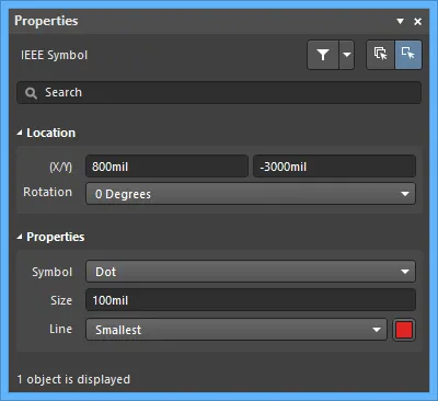
Location
Properties
-
Symbol - グラフィカルなIEEEシンボルを定義します。ドロップダウンリストからシンボルを選択します。
-
Size - IEEEシンボルの現在のサイズです。デフォルトサイズは 10 DXP Default Units (100mil)です。この値を増減してシンボルを大きく/小さくします。負の値を入力すると、シンボルは180度回転したように表示されます。
-
Line - シンボル外形を描画する線の幅です。
シンボルプロパティの定義
シンボルのデジグネータや説明などのプロパティは、Properties パネルの Symbol モードで編集します。
-
Designator - 必要なデジグネータのプレフィックスを入力し、その後に ? を続けます。プレフィックスは英字のみで構成することを推奨します。
-
Name および Description - これらの文字列は、シンボル検索を行う際に役立ちます。
-
Type このシンボルが表すコンポーネントの種類を定義します。会社ロゴ(Graphical)やヒートシンク(Mechanical)などの非標準コンポーネントも、回路図シンボルとして作成してプロジェクトに配置できます。
Component Type
設計環境では、完成したPCBに実装されるコンポーネントとは限らない設計エンティティを作成する必要がある場合もあります。たとえば、基板に接続される外部モジュールがあり、設計の明確化のためにコンポーネントとして描いて回路図に含めたいが、この基板のBOMには含めたくない場合があります。あるいは、ヒートシンクや取付ねじなどの機械部品はBOMに含める必要がある一方で、回路図には含めたくない場合もあります。
これらの状況は、コンポーネントの Type を設定することで管理します。先ほどの例では、コンポーネントタイプを Graphical に設定できます。もう1つの特殊なクラスとしてテストポイントがあります。これは回路図とPCBの両方に必要で、設計同期時にチェックされるべきですが、BOMには不要です。この場合、コンポーネントの Type は Standard (No BOM) に設定します。

非標準タイプのコンポーネントについては、Type を適切に設定してください。
コンポーネントをBOMに含めるかどうかの判定に使われるだけでなく、Type フィールドは、コンポーネント同期中にそのコンポーネントをどのように扱うかの判定にも使用されます。Standard、Net Tie、Jumper の各Typeは完全に同期され、コンポーネントは回路図からPCBへ渡され、ネット接続性がチェックされます。Mechanical および Graphical Type では、コンポーネントは回路図からPCBへ渡されません。これらのTypeのいずれかを持つコンポーネントがPCB上に手動配置され、対応する Type オプションが選択されている場合、コンポーネントレベルの同期は実行されますが、ネットレベルの接続性チェックは実行されません。
各種 Type オプションの詳細は、Propertiesパネルの Component mode を参照してください。
コンポーネントを複数パートに分割する
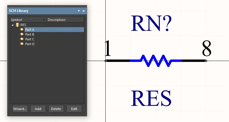
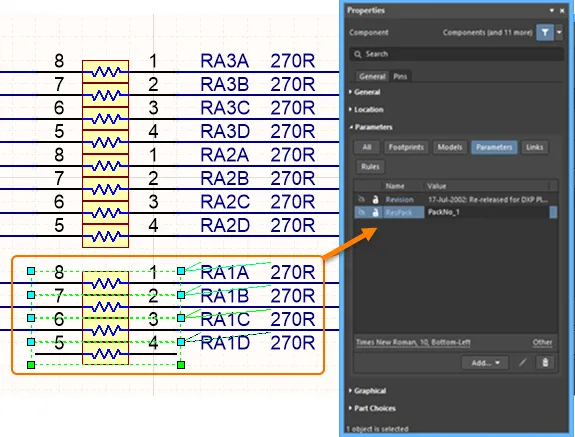
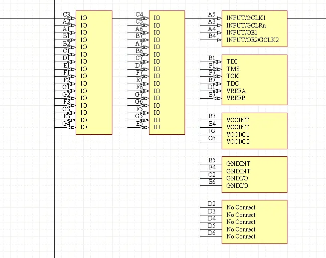
場合によっては、コンポーネントを複数のシンボルに分割する方が適切です。各シンボルは Part と呼ばれます。例として、8個の個別抵抗を含み、それぞれを独立して使用できる抵抗ネットワーク、リレーのコイルと接点セット、またはコネクタの各ピン(たとえば、配線を1つのコネクタシンボルにまとめて引き回すのではなく、シート全体にコネクタピンを配置したい場合)などがあります。別の例として、74F08SJX(2入力ANDゲート×4)があります。このデバイスには独立した2入力ANDゲートが4つあります。4つすべてを示す単一シンボルとして描くこともできますが、各ゲートを独立して回路図上の任意の場所に配置できるよう、4つの別々のゲートとして描く方が有用です。
これらのコンポーネントは multi-part components と呼ばれます。各パートは回路図ライブラリエディタで個別に作図し、それに応じてピンを追加します。下の画像は、同じ抵抗ネットワークを単一パートとして描いた場合と、4つの別パートとして描いた場合を示しています。

同じ抵抗ネットワークを、左は単一パート、右は4つの別パートとして示しています。
マルチパートコンポーネントを扱う際の注意点:
-
回路図シンボルエディタでは、メインメニューの Tools » New Part コマンドを使用して、現在のコンポーネントに別パートを追加します。あるいは、Active Bar の  ボタンをクリックするか、デザインスペースで右クリックしてコンテキストメニューから Tools » New Part を選択します。新しいパートがコンポーネントに追加され、そのパート用の空白シートが開かれて設計ウィンドウでアクティブになります。このシートを使用して、パートのグラフィカル表現を構成するプリミティブを追加します。
-
下図のように、SCH Library パネルを使用してマルチパートコンポーネント内のパート間を移動します。
また、デザインスペースの右クリックメニューから Tools » Next Part および Tools » Previous Part コマンドを使用して、次/前のパートを表示することもできます。
-
現在のドキュメントで開いているマルチパートコンポーネントからアクティブなパートを削除するには、メインメニューから Tools » Remove Part を選択するか、右クリックしてコンテキストメニューから Tools » Remove Part を選択します。SCH Library パネルから直接、マルチパートコンポーネントのパートを削除することもできます。
削除したコンポーネントのパートは、Undoコマンドでは復元できません。
-
コンポーネントのパートがわずかに異なる場合、パート間で内容をコピー&ペーストし、たとえば新しいパートではピン情報だけを更新する、といった運用が可能です。
-
回路図シンボルエディタでは、コンポーネントあたりのパート数に制限はなく、コンポーネントレベルの Alternate Display Mode feature を使用することで、各パートは異なるグラフィカル表現をサポートできます。また、定義されたNormal/Alternateモードを用いることで、単一のコンポーネントだけで、マルチパートコンポーネントを単一シンボル(全パート)としても、複数シンボル(各パート)としても表現できます。— learn more。
-
マルチパートコンポーネントのデジグネータには、各パートを識別するためのサフィックスが含まれます。サフィックスは英字または数字で、Preferences ダイアログの Schematic - General ページ にある Alpha Numeric Suffix 領域で設定します。なお、このオプションはソフトウェアのインストール環境設定であり、ライブラリや回路図ファイルには保存されません。そのため、設計ファイルと一緒に持ち運ばれることはありません。
-
マルチパートコンポーネントは同種(homogeneous)と見なされ、設計アノテーション時にはすべてのパートが等価で、アノテーション処理中に入れ替えられる可能性があります。たとえば、回路図シート上での相対位置に応じて、リレーのコイルがリレー接点セットと入れ替えられることがあります。配置済みコンポーネント内の特定パートを固定するには、下図のように Properties パネルで  を有効にします。
-
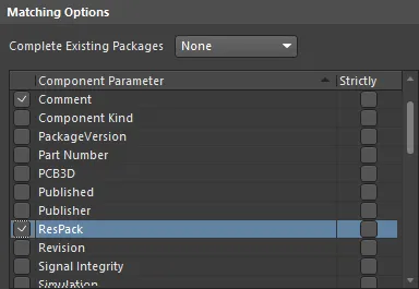
回路図のアノテーション中、マルチパート・コンポーネント内の各パートは、Annotate ダイアログ で設定された Matching Options に従って、1つのコンポーネントとしてまとまるようにパッキングされます(下図参照)。左側で有効になっているチェックボックスにより、パート同士をまとめてパッキング可能とするために一致している必要があるコンポーネント・プロパティが決まります。たとえばフィルタ設計におけるオペアンプ2個の組のように、特定のパートが同一の物理コンポーネント内に一緒に入るようパッキングを制御したい一方で、手動で割り当ててロックすることは避けたい場合は、そのコンポーネントに追加パラメータを付与し、どのパート同士をまとめるかを定義する値を入力してください。下の上側の画像は Annotate ダイアログの一致オプションを示しています。有効なパラメータはマルチパート・コンポーネントの一致判定に使用され、抵抗をパッケージへまとめる(同じパラメータ値を持つパートは同一の物理コンポーネントにまとめられる)ために、Properties パネル(下側の画像)で ResPack パラメータが追加されています。Strictly オプションに注意してください。このオプションが有効な場合、パーツはこのパラメータを must 含んでいるときに一緒にパッキングされます。異なる種類のマルチパート・コンポーネントでパッキング制御を行っている場合、このオプションには注意が必要です。Strictly is enabled の場合、対象となるすべてのコンポーネントがそのパラメータを含んでいなければなりません。
-
PCB のパート・スワップは、パートがマルチパート・コンポーネントとして定義されているコンポーネントに対してのみ実行できます。詳細は Pin Pair and Part Swapping ドキュメントを参照してください。
-
電源ピンを定義するには、コンポーネントに追加のパートを作成し、そのパート上に VCC と GND のピンを配置できます。再アノテーション時にどのゲートともスワップされないよう、Properties パネル の  オプションを有効にすることを忘れないでください。
表示モード – 同一コンポーネントの複数の表現
本ソフトウェアは、同一コンポーネントに対して異なる表示表現をサポートします。これらの表現には、DeMorgan 表現や IEEE 表現など、コンポーネントの異なるグラフィカル表現を含めることができます。あるいは、たとえば抵抗器を長方形で描くことを好む顧客もいれば、波線を好む顧客もいます。
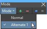
これらの表現はそれぞれ表示 Mode と呼ばれます。パートの代替ビューが追加されている場合、回路図シンボル・エディタの設計ウィンドウで、メインメニューの Tools » Mode サブメニューおよび Mode ツールバーの Mode ドロップダウンから代替モードを選択することで、編集用に表示されます。アクティブなコンポーネントの現在のグラフィカル表現は、メインメニューの該当項目、または Mode toolbar の Mode drop-down list にある項目の横に有効な「チェック」アイコンが表示されることで示されます。ただし、メニューおよびツールバーに一覧表示される代替グラフィカル・モードは最初の20個のみです。
メインメニューまたはツールバーのドロップダウンから通常モード/代替モードを選択するだけでなく、メインメニューの Tools » Mode » Previous および Tools » Mode » Next コマンド(Mode toolbar 上の  および
および  ボタン)を使用して、アクティブなコンポーネントの前/次のモードを表示することもできます。

2つの表示モードで作成された抵抗器。ライブラリ・エディタには Mode ツールバーがあり、モードの追加/削除や、モード間の切り替えに使用できます。
代替ビューモードを追加するには、回路図シンボル・エディタの設計ウィンドウにコンポーネント・パートを表示した状態で Tools » Mode » Add を選択するか、Mode toolbar の  ボタンをクリックします。
Alternate N 表示用の空白シートが表示されます(N は範囲 1-255 内で次に利用可能な番号です)。通常は、Normal mode で作成したパートをコピーし、新しい Alternate mode に貼り付けます。Edit » Copy と Edit » Paste を使用して Normal mode を Alternate mode. にコピー&ペーストします。これにより正しいピン一式が得られ、必要に応じてグラフィカル要素を変更し、ピン位置を調整できます。
現在の代替モードの名称を変更するには、メインメニューから Tools » Mode » Rename コマンドを選択するか、Mode toolbar の Rename をクリックします。コマンドを起動すると Rename Alternate Representation ダイアログ が表示されます。選択したシンボルの新しい名前を入力し、OK をクリックします。以後、この代替モードはメインメニューおよび Mode toolbar で定義した名前として表示されます。
アクティブなコンポーネントの現在のグラフィカル表現(モード)を削除するには、メインメニューから Tools » Mode » Remove コマンドを選択するか、Mode toolbar の  ボタンをクリックします。コンポーネントに存在する任意のグラフィカル表現(Normal および Alternate)を削除できます。コンポーネントに1つ以上の代替表現があり、Normal 表現を削除した場合、最初の代替(Alternate 1)が Normal 表現になります。その他の代替はそれに応じて番号が振り直されます。代替表現が存在しないコンポーネントで Normal 表現を削除すると、確認ダイアログでライブラリからコンポーネントを削除するか確認されます。Yes をクリックすると、実質的にライブラリからコンポーネントが削除されます。
必要なモードは、Properties パネル の Graphical region にある Mode selector を使用して、ライブラリから回路図シートへコンポーネントを配置する際に選択します。デフォルトの配置モードは、ライブラリが最後に保存されたときにライブラリ・エディタで表示されていたモードです。
各モードには同一のピン一式が含まれていなければなりません。そうでない場合、プロジェクト検証時に警告が生成されます。これは、当該コンポーネントに関連付けられた各フットプリントに対して定義できる pin-to-pad mappings が1セットのみであるためです。ピンは各モードで同じ位置にある必要はありません。
代替モードを持つマルチパート・コンポーネントの使用
Altium Designer は、定義された Normal および Alternate Modes を用い、単一のコンポーネントだけでマルチパート・コンポーネントを単一シンボル(全サブパート)または複数シンボル(各サブパートごとに1つ)として提示することをサポートします。たとえばデュアル・オペアンプは、ある表示モードでは2つのシンボルで表し、別の表示モードでは1つのシンボルで表すことができます(下図参照)。この場合、単一シンボル表示モードでは2番目のパートにプリミティブが存在しません。
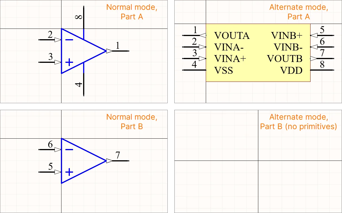
回路図シンボル・エディタでは、プリミティブを持たないパートは、SCH Library パネル で確認できるシンボル・パート一覧において、プリミティブを持つすべてのパートの下に列挙されている必要があります。
コンポーネント・レポートの生成
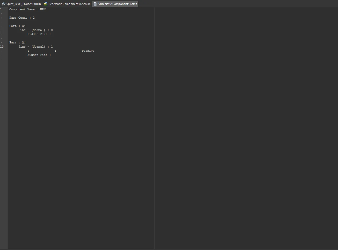
Component Report はアクティブなシンボルに関する情報を一覧表示します。
-
Reports » Component を選択します(ショートカット R, C)。
-
<LibraryName>.cmp というタイトルのレポートがアクティブ・ドキュメントとして開きます。ファイルにはコンポーネント名と、コンポーネントに含まれるパート数が含まれます。各パートについて、各グラフィカル表現(Normal および任意の Alternate)ごとのピン詳細が示されます。
-
レポートを閉じて回路図エディタのデザインスペースに戻ります。
ジャンパー・コンポーネントのサポート
ジャンパー(ワイヤリンクとも呼ばれます)は、配線(ルーティング)をジャンパー・コンポーネントに置き換えることを可能にし、片面基板を成功させる設計において重要な要素となることがよくあります。Altium Designer は、Jumper という特別なコンポーネント・タイプを通じてジャンパー・コンポーネントの使用をサポートします。
ジャンパーのフットプリントを PCB に直接配置することから始めることもできますが、推奨されるワークフローは回路図から開始します。詳細は Working with Jumper Components ページを参照してください。
回路図シンボル生成ツールの使用
コンポーネントの複雑化に伴い、コンポーネント・ライブラリのシンボルとそのピンデータを作成する作業はますます手間のかかるものになっています。たとえば、現行の大規模 BGA デバイスでは数百本のピンの配置と設定が必要となり、実用的なコンポーネント・シンボルを作成するには多大な時間と労力が必要になることが少なくありません。
コンポーネント・シンボル作成に伴う負荷を軽減するため、Altium Designer はシンボル・ウィザード・インターフェースとピン・エディタ・ダイアログに基づく高度な回路図シンボル生成ツールを提供します。これには、シンボル図形の自動生成、グリッド形式のピンテーブル、スマートなデータ貼り付け機能が含まれます。
シンボルの作成
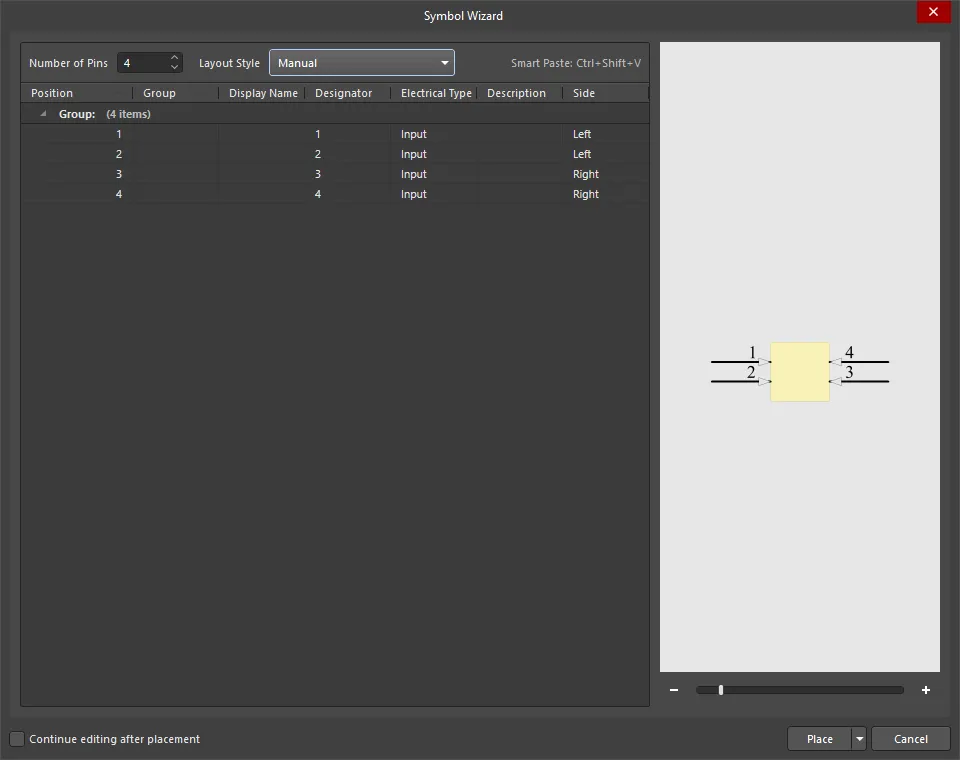
回路図シンボル生成ツールは、回路図ライブラリ・エディタでメインメニューから Tools » Symbol Wizard コマンドを選択することで利用可能になります。また、Component Editor in its Single Component Editing mode を使用して Workspace コンポーネントを作成する際にも、シンボル・モデルの下にあるボタンのドロップダウン・アイコンをクリックし、メニューから Wizard を選択することでアクセスできます。
ツールを使用して新しいコンポーネント・シンボルを作成するには、まずアクティブなライブラリドキュメントに新しいコンポーネントを追加します。次に、コマンドを起動すると開くツールのインターフェース(Symbol Wizard ダイアログ)で新しいシンボルを作成できます。ダイアログを使用して、ピン数、ピン配置レイアウト、ピンデータなど、必要に応じてコンポーネント・シンボルを対話的に定義します。
-
Number of Pins - 目的のピン数を手入力するか、上下矢印で増減します。
-
Layout Style - ピン位置が自動的に割り当てられる、事前定義パターンのセットから選択します。ドロップダウンで希望の配置を選択してください。右側の Preview 画像と、Side 列のデータがそれに応じて更新されます。選択肢には次が含まれます:
Grid
-
Position – シンボルピンの参照位置インデックスです。このデータは編集できません。
-
Group – ピンの集合グループを定義するために手入力する文字列です。
-
Display Name – コンポーネント・ピンの表示名属性文字列です。
スラッシュを含むピン名は代替ピン名として認識され、生成されたシンボルのピンプロパティに追加されます。なお、各ピン機能を区切るスラッシュ文字の使用はハードコードされているため、ピン名にスラッシュを含めたいがカスタムピン名を作成したくない場合(例: I/O)、シンボル作成後にプロパティパネルの Pin モードでこれらの追加ピン名を削除できます 。
-
Designator – ピンのデジグネータ属性文字列です。これはデフォルトでピン Position と自動的に一致します。
-
Electrical Type – フィールドのドロップダウンを使用して、ピンの電気タイプを選択します。選択肢には Input、 I/O、 Output、 Open Collector、 Passive、 HiZ、 Open Emitter、および Power.
-
Description が含まれます。 – ピンの説明文字列属性です。
-
Side – フィールドのドロップダウンを使用して、シンボルの位置を選択します。Left、 Bottom、 Right、および Top から選択します。この領域が変更されると、Layout style 設定は Manual に変わります。
列見出しをクリックすると、その列でグリッドデータを並べ替えます。もう一度クリックすると、昇順/降順が切り替わります。
表内では、標準的なコピー&ペースト操作で、あるセルグループのデータを別のセルグループへ入力できます。たとえば、列内の3セルを選択してデータをコピー(right-click – Copy)し、次に貼り付け先の3セルを選択して貼り付け(right-click – Paste)できます。 同じ手法で、スプレッドシート、テキスト、PDFファイルなど外部ソースからのデータ選択をコピーして貼り付けることもできます。
グリッドセルは、単一または複数を手動で編集できます。標準の Ctrl+click および Shift+click 操作を使用してください。ドロップダウンメニューを備えた列で複数セルを編集するには、目的のセル範囲を選択し、選択範囲内のいずれかのセルで新しいメニュー選択を行います。
右クリックメニュー
-
Move Up - 選択したデータを1行上へ移動します。
-
Move Down - 選択したデータを1行下へ移動します。
-
Copy - 選択したデータをクリップボードへコピーします。
-
Paste - クリップボードに最後にコピーしたデータを、カーソル位置へ貼り付けます。
-
Smart Paste - Pin Data Smart Paste ダイアログを開き、外部ソースデータの複数列をグリッド内の対応列へコピーします。ダイアログで列データと区切り文字を設定し、Paste をクリックします。Smart Paste の詳細を参照してください。
-
Clear - ピンデータを削除します。
Preview
この領域にはシンボル図形のプレビューが表示され、現在の設定とピンデータを動的に反映します。スライダーバー、または - と + を使用して図形を拡大/縮小します。
Additional Controls
-
Continue editing after placement - チェックすると、コンポーネント配置後もダイアログがアクティブのまま(さらに編集可能)になります。
-
Place - 完成したシンボルとピンデータを配置します。選択肢には次が含まれます:
-
Place Symbol
-
Place New Symbol
-
Place New Part
Pasting Pin Data
表内のピンデータは複数セルに対して共通値へ編集できますが、ダイアログの Paste および Smart Paste 機能を使うと、外部ソースから大量の異なるデータを取り込んで全セルデータを入力する、より高度な方法が利用できます。
表内では、標準のコピー&ペースト操作で、あるセルグループのデータを別のセルグループへ入力できます。たとえば、列内の3セルを選択してデータをコピー(右クリック - Copy)し、次に貼り付け先の3セルを選択して貼り付け(右クリック - Paste)します。
同じ手法で、スプレッドシート、テキストファイル、PDFファイルなど外部ソースからのデータ選択をコピー&ペーストすることもできます。
 外部スプレッドシートからコピーしたデータを Pin data テーブルへ貼り付ける例。
Smart Paste
標準のコピー&ペースト操作に加えて、Smart Paste は自動列マッピング方式を用いて、外部ソースから複数列のデータを入力する機能を提供します。
Pin data テーブルの対応列へソースデータの複数列をコピーするには、テーブル内で右クリックし、コンテキストメニューから Smart Paste コマンドを選択します。これにより Pin Data Smart Paste ダイアログが開き、ソースデータが取り込まれます。データ区切り文字は複数用意されており、ソースデータで使用されている区切り文字に合わせて選択できます。

Pin Data Smart Paste ダイアログ
Options and Controls of the Pin Data Smart Paste ダイアログ
Additional Controls
-
Paste - クリックして Smart Paste プロセスを完了します。 ソースデータは、グリッド領域で指定した対応列へコピーされます。
右クリックメニュー
-
Remove Line - 行の上でクリックしてこのコマンドを選択すると、その行を削除します。ダイアログ内の空白部分で実行した場合は、最下行が削除されます。
-
Remove Column - 列の上でクリックしてこのコマンドを選択すると、その列を削除します。
Symbol Placement
設定とピンデータを必要に応じて構成したら、シンボルをアクティブなライブラリコンポーネントのデザインスペースへ配置できます。配置は単一コンポーネントとして、またはマルチパートコンポーネントの1セクションとして行えます。これらはダイアログの Place ボタンに関連付けられたコンテキストメニューから利用できる各コマンドで実行します。Continue editing after placement オプションが有効な場合、コンポーネント/パート配置後も Symbol Wizard ダイアログはアクティブのまま(さらに編集可能)である点に注意してください。
回路図ライブラリ内の既存コンポーネントに対して Symbol Wizard ダイアログへアクセスすると、すべての設定とピンデータが表示され、追加変更が可能な状態になります。新規ライブラリコンポーネントに対して使用した場合にのみ、ダイアログはデフォルト状態で表示されます。
Smart Grid Insert Tool による回路図シンボル作成の高速化
SCHLIB List パネルで利用できる Smart Grid Insert ツールを使用すると、現在のクリップボードデータを Altium Designer のオブジェクトプロパティへマッピングできます。これらのツールにより回路図シンボル作成プロセスが大幅に簡素化され、スプレッドシート、PDF、ASCIIファイルなどの外部データから、数ステップでコンポーネントのピンを直接作成できます。
ソースのピンデータから Altium Designer へ直接コピーすることもできますが、最適な結果を得るために、少しだけ事前準備を行う価値があります。その作業にはスプレッドシートが適しています。通常、次のような少数の手順だけで十分です。
-
列間マッピングを容易にするためにヘッダー行を追加します。列名を完全に一致させる必要はありません。Altium Designer は正しいマッピングを自動推定するのが得意です。
-
Object Kind 列を追加し、Altium Designer がピン型オブジェクトを作成すべきであることを認識できるようにします。
-
Type 列を追加し、各ピンの電気タイプを指定します。
-
X および Y のピン位置を含めます。スプレッドシートにはセルへ値を埋める優れた機能があります。たとえば Microsoft Excel で右クリックしながらドラッグしてセル範囲を選択すると、必要な数値系列を指定できるため、回路図ライブラリ内でピン間隔を簡単に揃えられます。
FPGA のようにピン数が多く、規則的にセクション分けされたコンポーネントは、Altium Designer でマルチパートコンポーネントとして実装するのに適しています。最も簡単な方法は、Altium Designer のコンポーネントの最初のパートにすべてのピンを作成し、その後ピンのブロックを他のパートへ切り取り&貼り付けすることです。
ピンを整然とした「パート作成用」のグループにするには、スプレッドシート上で各パートのピンの間に空行を2行ほど挟んでみてください。座標値をどこでリスタートすべきかが見やすくなるだけでなく、大きな範囲に対して X、Y 値を自動で追加してから、空行に入った不要な X、Y 値を削除することもできます。これにより、削除した位置にはピンが作成されず、パート作成用のグループがきれいに間隔を空けて配置されます。

スプレッドシートのツールを使って、ピンに適切な X および Y 座標を追加します。
スプレッドシートで必要なセルを選択してコピーします。選択範囲に不要な列が含まれていても問題ありません。Smart Grid ツールはそれらを無視できます。
Altium Designer で SCHLIB List パネル内を右クリックし、メニューから Smart Grid Insert を選択して Smart Grid Insert ダイアログを開きます。ソースデータにヘッダー行が含まれている場合、Altium Designer はオブジェクト種別を自動的に識別しようとし、作成されるオブジェクトのリストを構築します。ここで覚えておきたい点として、列をマッピングする前の「作成されるオブジェクト」リストは、現在の Altium Designer のデフォルトのピンオブジェクトのプロパティを持っています。たとえば、すべてのピンを 180 度で長さ 20 にしたい場合は、Smart Grid を開始する前に Altium Designer 側でデフォルト値を設定しておきます。そうすれば、スプレッドシートにその設定を追加したり、作成後に Altium Designer で編集したりする必要がありません。デフォルトの設定方法が分からない場合は、メニューから Place » Pin を選択し、ピンを配置する前に Tab を押してデフォルト値を編集し、そのピンを1つ配置してから削除してください。
ヘッダー行を含めるもう1つの大きな利点は、Automatically Determine Paste ボタンを使えることです。これは非常に便利な機能で、作成されるオブジェクト内のフィールドをソースデータの列タイトルと検索・比較し、どのようにマッピングすべきかを賢く判断してくれます。自動機能が誤ったマッピングをしても心配はいりません。Undo Paste ボタンでマッピングした列を取り消せます。手動でマッピングするには、ソースデータの列と作成されるオブジェクト側の対応する列を選択し、Paste Column ボタンをクリックします。
OK をクリックするとすぐに、作成されたオブジェクト一式がデザインスペースに表示されます。各パートに適切なボディを追加し、切り取り&貼り付けで個別のパートを作成すれば、シンボルの完成です。

Smart Grid で挿入されたピンと、コンポーネントボディを追加したパート。

 AI で翻訳