A printed circuit board is not fabricated as a single entity; typically a number of boards are fabricated on a panel. The panel can be defined by the fabricator, or alternatively, the board designer can create a panel in the PCB editor, using a feature referred to as an Embedded Board Array, also known as panelization.
An Embedded Board Array is a primitive design object that you place into the PCB design space and link to an existing board file. The Embedded Board Array stamps out the linked board from 1 to n times at the specified spacing. By placing multiple Embedded Board Arrays, you also can create a fabrication panel of different boards, or the same board can be laid out in a step and turn pattern.
The image below shows a board repeated eight times in a step and turn pattern (alternate boards flipped). This was created by placing two Embedded Board Arrays; one with the boards facing up and the other with the boards flipped. The layer stack, dimensioning, V-groove, and route information has been added in this file rather than in the original source PCB.
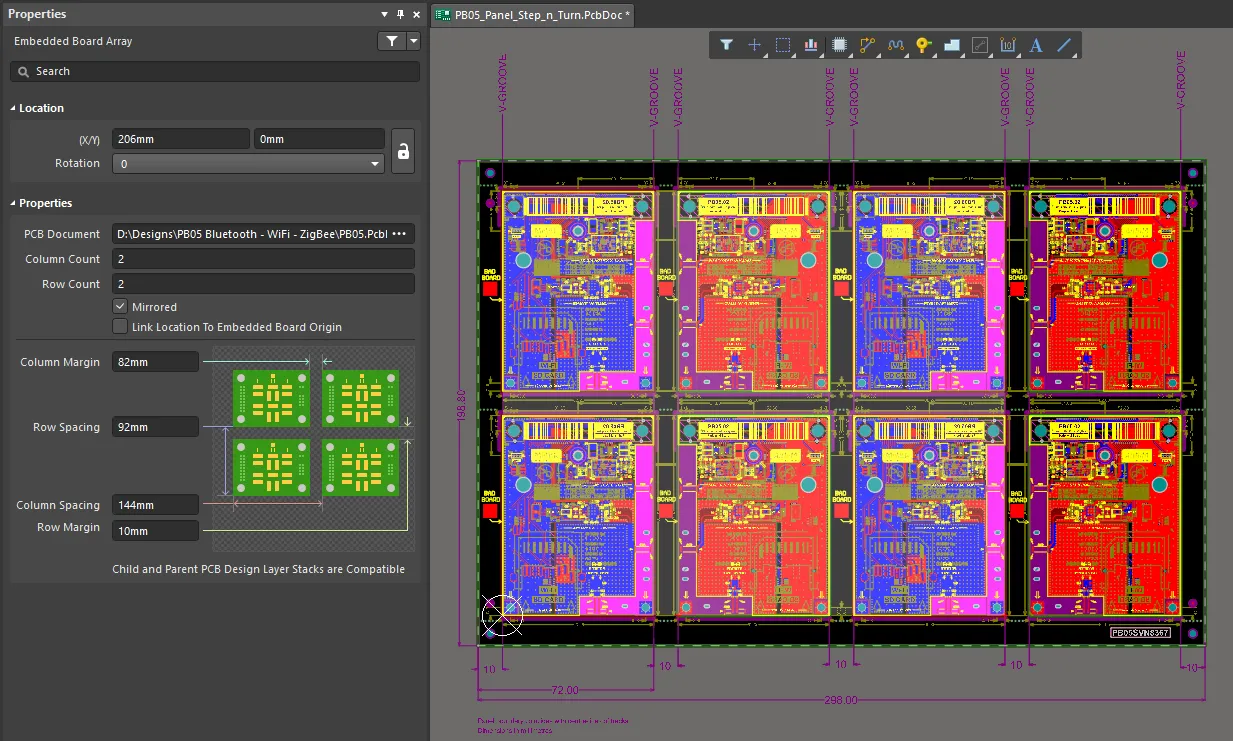
Since the Embedded Board Array links to the source PCB, any design changes made in the source PCB are loaded into the Embedded Board Array the next time the array board file is opened.
A key part of the panelization process is defining how the individual boards are to be separated. There are two common approaches: V-groove panelization or breakaway-tab panelization. V-groove panelization is inexpensive and effective for rectangular shaped boards; non-rectangular boards must use breakaway tabs.
To create breakaway-tab panelization, define a route tool path slot around the edge of each board, leaving small sections of remaining board that are perforated by a series of small holes, as shown in the adjacent image.
The route tool path is defined by placing track objects on a mechanical layer, which is then nominated as the Route Tool Path layer in the Properties panel (also shown in the image). Use the Create Primitives from Board Shape command to outline the board shape with tracks/arcs that define the route tool path, then edit them as required to create the breakaway tab regions. The breakaway tabs, also referred to as mouse bites, are created by placing a row of small unplated pads.
To learn more about panelization, read these excellent, detailed panelization guidelines, published on the Electronic Design website.
Placement
After launching the embedded board array command (Place » Embedded Board Array/Panelize), the cursor will change to a crosshair and you will enter embedded board array placement mode. The location of the crosshair decides the lower-left corner of the board array.
- Position this corner of the array at the required location then click or press Enter to place.
- Continue placing further embedded board arrays or right-click or press Esc to exit placement mode.
If a placed array does not yet reference a PCB document, there will be only a red crosshair to represent the blanket array.
Verification of Layer Stack Compatibility
When building a panel, it is important that you ensure the layer stackup for each referenced child board is compatible with the stackup for the parent board onto which the panels are placed. When you choose the reference PCB design for the embedded board array being placed, Altium Designer will compare the layer stacks of that board with that of the active PCB into which you are placing the array. The result of this comparison will be presented in the Embedded Board Array mode of the Properties panel:
- If the layer stacks are compatible, the following text will be displayed: Child and Parent PCB Design Layer Stacks are Compatible.
- If the layer stacks are not compatible, the following text will be displayed: Child and Parent PCB Design Layer Stacks are NOT Compatible.
If you choose the reference PCB design for the embedded board array during placement (by pressing Tab after selecting the Embedded Board Array placement command and selecting the PCB from the Properties panel), the Warning! dialog will open if the layer stacks are not compatible. You have the choice to manually resolve the discrepency at a later stage (the Synchronize Manually Later option); a reminder will be generated if you attempt to generate fabrication output. Alternatively, you can get Altium Designer to automatically attempt to resolve layer stack compatibility issues (the Synchronize Automatically Now option). The automatic layer stack synchronization process will attempt to:
- Ensure that all required child board layer stack ordered layers exist in the parent board (the PCB file containing the embedded board array).
- Modify the parent board layer stack in an attempt to achieve synchronization; a child board is never modified.
- Make only additive or layer type modifications to the parent board; layers are never removed.
When non-compatible layer stacks are detected in the panel, an issue will also appear on the Health Check tab of the Properties panel in its Board mode. Learn more about the PCB Health Check Monitor.
You can also generate a Stackup Compatibility report from the active PCB panel document. This report gives feedback on the layer stackup of each board defined on the panel, as well as the layer stackup defined for the panel itself. If there is at least one embedded board array placed on the PCB document, you can access the Reports » Stackup Compatibility Report command from the main menus. After launching the command, a report - Embedded Boards Stackup Compatibility - <PCBDocumentName>.html - is generated and opened as the active document. Where incompatibilities exist, the report provides a summary of how many incompatible layers have been found within the embedded boards placed on the panel document. A compatibility table is also presented, which visually displays the stacks of the embedded boards and the panel itself. Any incompatible layers are highlighted with red text.
The table also provides hyperlinks to open the Layer Stack Manager for each PCB (and the panel), so you can examine the stackups and determine how to resolve the incompatibilites. Clicking one of these links will first make the corresponding PCB document the active document then open the Layer Stack Manager.
The report is also generated in .txt format. Both report formats are stored in the folder specified by the Output Path entry on the Options tab of the Options for Project dialog. Only the HTML-formatted report is added to the parent project in the Projects panel, and can be found in the Generated\Documents sub-folder.
Graphical Editing
This method of editing allows you to select a placed embedded board array object directly in the design space and change its location or orientation graphically.
When an embedded board array object is selected, it is distinguished by a light gray background. The below images illustrate an un-referenced board array (first image) and a 2 x 2 array that references a single PCB design (second image).

An un-referenced board array

A 2 x 2 array that references a single PCB design
Click anywhere within the boundary of the array then drag to reposition it. The array is automatically 'grabbed' by its lower-left corner and the board array's location is used as the anchor point to the cursor. The embedded board array can be rotated or flipped while dragging in the following ways:
- Press the Spacebar to rotate the embedded board array. Rotation is counterclockwise.
- Press the L key to flip the embedded board array to the other side of the board.
Notes
- The embedded board array(s) used to create a representation of the manufacturing panel should be placed on a separate PCB document within the existing or alternate PCB project. This document should be considered the manufacturing 'hub' for other PCB documents that contain the actual designs.
- You can place additional objects to support panel manufacturing (for example, free pads as tooling holes), however, it is not advisable to place any other objects that would represent the actual physical design within the same document as the embedded board array(s).
- Since the embedded board array object references a PCB design file rather than containing a pasted copy of it, the source PCB design may be modified at any time. Once the reference file is saved, refresh the view of the panel document in order to bring the panel up-to-date.
- If a placed array does not yet reference a PCB document, there will be a green rectangular bounding box with the text No source at its center along with a small cross to mark the lower-left corner of the array.
- Gerber, NC Drill, ODB++, and printed output can be generated from a panel of embedded board arrays.
- When using the Design » Board Shape » Create Primitives From Board Shape command's Route Tool Outline option, you also can select the Include Cutouts option to simulate tool paths that contour board cutout edges.
- The software automatically attempts to resolve layer stack compatibility issues. The automatic layer stack synchronization process will attempt to:
- Ensure that all required child board layer stack ordered layers exist in the parent board (the PCB file containing the embedded board array).
- Modify the parent board layer stack in an attempt to achieve synchronization - a child board is never modified.
- Make only additive or layer type modifications to the parent board, layers are never removed.
- Note that the counterhole features are not currently supported by an embedded board array and its Drill Table and Hole Size Editor.
Embedded Board Array Properties
General Tab
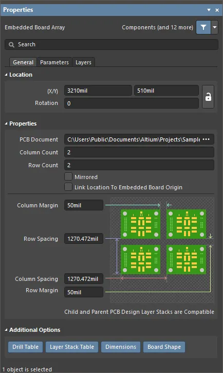
Location
The

icon to the right of this region must be displayed as

(unlocked) in order to access the below fields. Toggle the lock/unlock icon to change its lock status.
- (X/Y)
- X (first field) - the current X (horizontal) coordinate of the reference point of the embedded board array, relative to the current design space origin. Edit to change the X position of the embedded board array. The value can be entered in either metric or imperial, include the units when entering a value whose units are not the current default.
- Y (second field) - The current Y (vertical) coordinate of the reference point of the embedded board array, relative to the current origin. Edit to change the Y position of the embedded board array. The value can be entered in either metric or imperial, include the units when entering a value whose units are not the current default.
- Rotation - the embedded array's angle of rotation (in degrees) measured counterclockwise from zero (the 3 o'clock horizontal).
Properties
- PCB Document - displays the path to the current reference PCB document that will be used to populate the array. Click
 to browse for a different PCB document.
- Column Count - displays the number of columns in the board array. Edit this field to define the number of columns in the array.
- Row Count - displays the number of rows in the board array. Edit this field to define the number of rows in the array.
- Mirrored - enable to horizontally mirror the board array.
- Link Location to Embedded Board Origin - enable to reference the board array/panelization from the origin of the embedded board. Disable (default) to build the array based on the bottom left point of the objects in the referenced board's design space.
- Column Margin - displays the current column margin between edges of PCBs in the array. Values can be defined in either
mm or mil units. To specify the units when entering a number, add the mm or mil suffix to the value.
- Row Spacing - displays the current vertical pitch between PCBs in the array. The space between two adjacent boards is the pitch minus the height of one board. Edit this field to change the board pitch. Values can be defined in either
mm or mil units. To specify the units when entering a number, add the mm or mil suffix to the value.
- Column Spacing - displays the current horizontal pitch between PCBs in the array. The space between two adjacent boards is the pitch minus the width of one board. Edit this field to change the board pitch. Values can be defined in either
mm or mil units. To specify the units when entering a number, add the mm or mil suffix to the value.
- Row Margin - displays the current row margin between edges of PCBs in the array. Values can be defined in either
mm or mil units. To specify the units when entering a number, add the mm or mil suffix to the value.
Additional Options
Enable the additional objects you would like displayed or hidden, by type. If the button is blue, that type of object will be displayed.
Note that Special Strings placed in the embedded board array PCB file can also have their Special String name superimposed displayed/hidden, by enabling/disabling the Special Strings button in the Additional Options section of the View Options tab of the View Configuration panel. This superimposed name feature does not work for special strings embedded in the source PCB file, only those placed in the embedded board array PCB file.
Parameters Tab
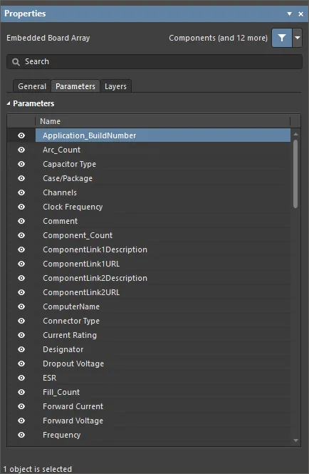
Table - displays the Name of each listed parameter. Use the  icon to enable or disable the parameters.
Layers Tab

Table - displays the Name and Type of all layers from the linked PCB. Use the icon to enable or disable the layers.
Keepout objects placed in a PCB design can also be shown in a panelized embedded board array using the PCB as a source. Note that this feature only provides a visual representation of the Keepout layer - copper objects will not respect keepouts from the source PCB when placed on the Embedded Board Array.
