 Документация Altium Designer
...
Advanced Design Environment Topics in Altium Designer
Взаимодействие с другими системами проектирования
Документация Altium Designer
...
Advanced Design Environment Topics in Altium Designer
Взаимодействие с другими системами проектирования
Interfacing to the TASKING Tools from Altium Designer
The TASKING Pin Mapper provider extension provides bi-directional communication between Altium Designer's PCB Editor and your TASKING toolset's Pin Mapper tool. This allows you to interactively perform pin-swapping within the Altium Designer PCB design workspace, and dynamically synchronize changes with your TASKING Pin Mapper tool. This ensures that your TASKING embedded source code is kept in-sync, without the need to export and import change files.
TASKING Pin Mapper Wizard
The Tasking Pin Mapper Wizard enhances design collaboration between the TASKING VX-toolset for ARM® and Altium Designer. In today’s complex processor devices, the pin functionality and internal connectivity are configured by internal processor registers, as defined in the embedded design phase. In order to create a complete product design, that unique processor configuration needs to be represented in a schematic document of a PCB design project.
The Tasking Pin Mapper Wizard facilitates data synchronization from the tool’s own Pin Mapper to a schematic document. The resulting schematic document will reflect the device pin configurations that have been assigned in the TASKING VX-toolset for ARM’s Pin Mapper, as saved in its Pin Configuration file (*.pincfg).
The Tasking Pin Mapper Wizard provides a direct data path from an embedded software project based on an ARM processor in the TASKING VX-toolset for ARM and its PCB project representation. The transferred design data includes identifying information, such as the processor chips, pin assignments to peripherals, electrical pin attributes, and symbolic names.
The Tasking Pin Mapper Wizard defines the VX-toolset’s Pin Mapper file (*.pincfg) to extract this information, then places an appropriately configured component on a new or existing schematic document. The component itself is sourced from a suitable Integrated Library.
The TASKING Pin Mapper wizard is accessed from the schematic editor by choosing the Tools » Tasking Pin Mapper command from the main menus.
The following pages of the wizard lead you through the process of creating a schematic from a specified TASKING Pin Mapper file.
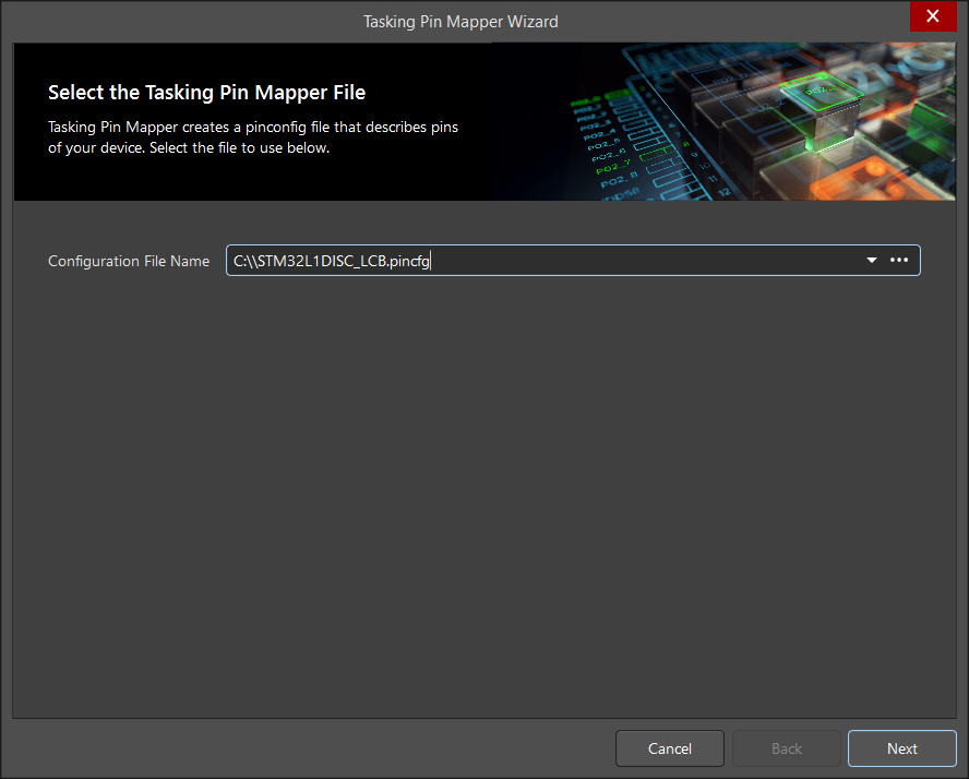
Select the TASKING Pin Mapper File
Once the opening dialog is dismissed, the source pin configuration file (*.pincfg) from the VX-Toolset’s Pin Mapper can be selected. Use the  button to locate and load the desired tasking Pin Mapper file.
Select Component
The Select Component page will, if possible, populate with available options for the processor device.
If the Tasking pin mapper file has specified an explicit processor type, the system will attempt to locate it in the available Altium Designer libraries. Alternatively, if the pin file defines a processor family (say, the ST Microelectronics STM32_T2 family of ARM Cortex processors) the list will contain all compatible types from the Altium Designer library - select the desired processor variant from the list.
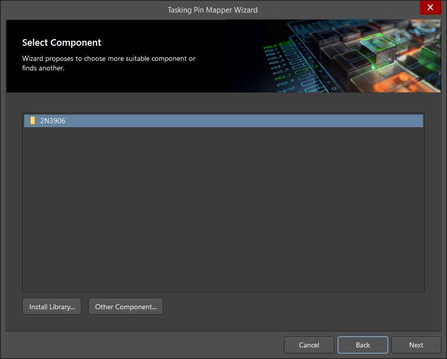
The processor list will be blank if a compatible processor library is not loaded or available in Altium Designer. Use the 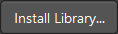 button to locate and install a suitable Integrated library.
To select a different processor from that offered by the list, use the 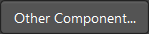 button to open the Browse Libraries dialog. Select the desired library from the Libraries drop-down menu and choose a suitable processor component from the list.
In the case where an explicit processor has been defined in the pin mapper file, or has been selected from a library using the Other component function, the list will show a single entry for the processor component.
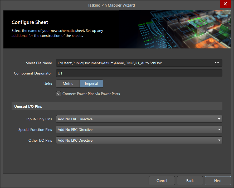
Configure the Sheet
The Configure the Sheet page defines the properties and behavior of the generated processor schematic.
Since the source pin mapper file defines both the pin functionality and external connections, its representative schematic needs to be configured to present that information in a way that is compatible with the target PCB design project. As such, this means basic name settings through to how pins, ports and compiler directives are handled.
The schematic sheet configuration includes the following settings:
- Sheet file name – the proposed schematic file name. Use to define or locate an alternative schematic file.
- Component Designator – the designator for the selected processor component. Edit as required.
- Units – Select the appropriate units for the schematic document.
-
Connect Power Pins via Power Ports – automatically connect the design's Power pins to standard Power Ports.
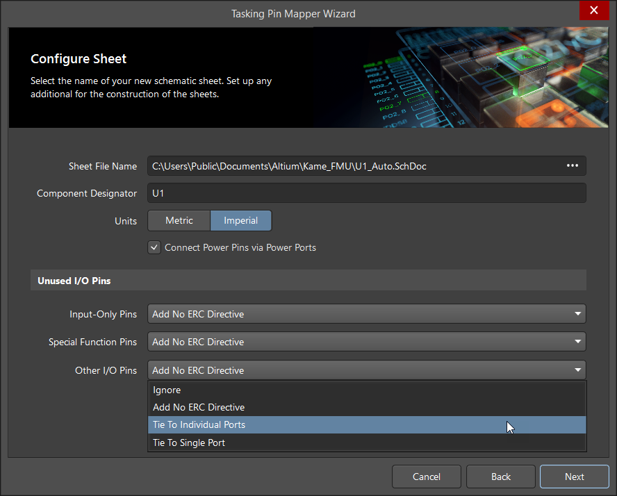
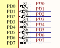
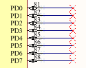
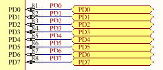
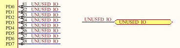
- Unused I/O pins – configure how unassigned processor I/O pins will be presented on the schematic.
-
Ignore – do not configure unused processor I/O pins.
-
Add No ERC Directive – prevent Electrical Rule Checks on unused I/O pins by placing No ERC directive objects.
-
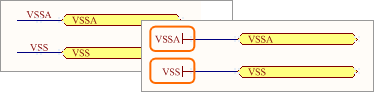
Tie to individual ports – connect corresponding ports to unused I/O pins.
-
Tie to Single port – assign unused I/O pins to one port object.
-
Place
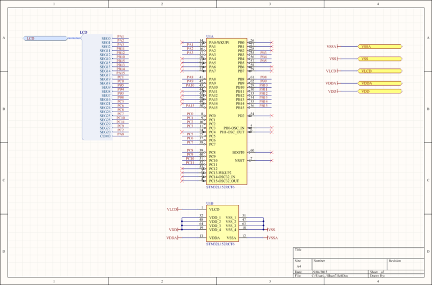
This, the final page of the wizard, provides a summary of the selected settings. After clicking the  button, the new processor schematic document is added to the current project and opened in Altium Designer's schematic editor. The schematic will contain your microprocessor, with all of your original pin signal names and configurations.
TASKING Pin Net Swapping
A component pin is swappable with another pin in that component when both pins have the same Pin Group. The swapping feature supports more than just pins; it also supports swapping a partially routed net. This is ideal if you are working on a dense board and escape routing from the components at both ends of a connection. When you perform a pin swap any connected routing is also swapped to the target net.
The PCB editor includes commands to interactively perform pin-swapping within the PCB design space, and dynamically synchronize changes with your TASKING Pin Mapper tool.
- The Tools » Pin/Part Swapping » Interactive TASKING Pin/Net Swapping command accessed from the main menus of the PCB editor is used to interactively perform pin-swapping within the PCB design space. After launching the command, everything in the PCB workspace is masked (faded) except those pins that are swappable. Keep an eye on the Status Bar. It will prompt you for the next action: Choose Sub-Net to move. After clicking on a swappable pin, you will be prompted to choose a target net for the sub-net to swap. All possible target pins that can be swapped will be highlighted. Click on the target pin to complete the swap action. You will then be ready to perform another pin swap, if required.
- The TASKING PinSwap command accessed from the PCB editor by right-clicking over the required pad of a component and selecting the command from the context menu is used to interactively perform a single pin swap for the component pin (pad) currently under the cursor. After launching the command, everything in the PCB workspace is masked (faded) except those pins that are swappable. Click on the target pin to complete the swap action.
As you make pin swaps within the PCB document, those changes are passed dynamically to your TASKING Pin Mapper tool, courtesy of the bi-directional communication support provided through the TASKING Pin Mapper Provider software extension. This ensures that your TASKING embedded source code is kept in-sync without the need to export and import change files.